
TOWARD THE OPTIMAL ARCHITECTURE
OF AN ASIC FOR NEUROSTIMULATION
Mario A. Meza Cuevas, Lait Abu Saleh, Dietmar Schroeder and Wolfgang Krautschneider
Institute of Nanoelectronics, Hamburg University of Technology, Eissendorfer Strasse. 38, Hamburg, Germany
Keywords: Neurostimulation, Electrical stimulation, Stimulation waveform, Implant, Current stimulation, Dac, Current
steering.
Abstract: Electrical Neurostimulation has been effective in several medical therapies and also for restoring
physiological, sensory and neuromuscular deficits. The rectangular pulse waveform has been used as a
standard shape for neural stimulation. However, it has been shown that non-rectangular waveforms provide
a more energy-efficient neural stimulation. An ASIC has been developed composed of a stimulator, capable
of driving several current waveforms, and an analog channel for biosignal acquisition. The design is
implemented in 130 nm / 1.2 V CMOS technology, requiring a silicon area of 0.696 mm
2
. Experimental
results show that the stimulator can generate analog signals from a digital input of 8 bits. The output stage
can drive up to ±9.8 µA, with a DNL and INL of 0.47 and 1.05 LSB, respectively. Its SFDR is 50.2 dB. And
it consumes a maximum of 128.12 µW. The analog input channel presents a power consumption of 140
µW, a gain of 52.2 dB, a bandwidth of 0.5 – 1130 Hz and 10 µV
rms
of noise.
1 INTRODUCTION
Electrical Neurostimulation has been effective in
reducing symptoms of some neurological disorders
by applying Vagus Nerve Stimulation (VNS) in case
of epilepsy and depression (Rush, 2000; Milby,
2009), or also by employing Deep Brain Stimulation
(DBS) in case of Parkinson´s, epilepsy, depression
or dystonia; for alleviating some types of chronic
pain (Barolat and Sharan, 2004); for assisting
physiological functions through biomedical devices
such as the pacemaker, bladder prosthesis and the
phrenic pacer (Ba, 2003; Haddad, 2006; Lin, 2008);
for restoring sensory deficits, such as vision through
retinal, optical nerve, Lateral Geniculate Nucleous
(LGN), or cortical implants (Dobelle, 2000; Veraart,
2003; Pezaris, 2007; Graf, 2008), or hearing through
cochlear implants (Rubinstein, 2004); and for
restoring the movement of extremities by using
Functional Neuromuscular Stimulation (FNS) in
patients that suffer neuromuscular deficits caused by
spinal cord injury, multiple sclerosis or stroke
(Peckham, 1981; Ring, 2005; Garcia Blanco, 2007;
Pohlmeyer 2009).
In all those cases the system shall fulfill certain
characteristics regarding physical design, small
systems are preferable due to the necessity of the
implantation of the system into the human body.
Due to the size and location of the implanted
devices, most of them are powered by an inductive
link. Thus, the energy transfer is limited, therefore,
low-power considerations play an important role in
design of implanted biomedical systems. To support
power efficiency and the use of advanced CMOS
technologies, the operation voltages should be as
small as possible. Similarly, it is important to
maintain low power dissipation, since the increase of
temperature in tissues or brain could be harmful.
The stimulation signals could be either current or
voltage signals, but most commonly used are current
signals since the natural stimulation is performed
through electrical current. Besides, current pulses
are preferred over voltage pulses to eliminate
variations in the stimulation threshold as a result of
the changes in the electrode-tissue impedance.
The rectangular pulse waveform has been used
as standard shape for neural stimulation. However,
through simulations, some authors have shown that
non-rectangular waveforms can provide more
energy-efficient neural stimulation and also reduce
stimulation artifacts (Bennie, 2002; Mandrile, 2003;
Jezernik, 2005; Robillard, 2006; Sahin, 2007). While
the strength-duration curve is defined for rectangular
pulses, different pulse shapes shift the chronaxie
179
Meza Cuevas M., Abu Saleh L., Schroeder D. and Krautschneider W..
TOWARD THE OPTIMAL ARCHITECTURE OF AN ASIC FOR NEUROSTIMULATION.
DOI: 10.5220/0003774001790184
In Proceedings of the International Conference on Biomedical Electronics and Devices (BIODEVICES-2012), pages 179-184
ISBN: 978-989-8425-91-1
Copyright
c
2012 SCITEPRESS (Science and Technology Publications, Lda.)
time. Thus, by injecting longer pulses, it is possible
to improve the charge injection of the electrodes and
also to reduce the threshold charge and threshold
energy.
It is desirable to stimulate small groups of
neurons or even single neurons. Thus, it is
convenient to build small electrodes in order to
achieve high selectivity. However, with smaller
electrodes, higher stimulation voltages are required,
due to the electrode impedance. Through current
stimulation with different waveforms it is possible to
reduce the voltage peak of the injected signal
necessary to achieve the firing of an action potential
(Halpern, 2009). This also reduces some phenomena
at the electrodes such as hydrolysis and metal
corrosion.
It was also demonstrated that the waveform and
frequency of the signal have certain influence on the
selectivity of stimulation of neurons with their cell
bodies near the electrode and fibers of passage
(Grill, 1995; McIntyre 2000, 2002).
An ASIC was developed to enable
experimentation by stimulating neurons with
different current waveforms, amplitudes and
frequencies. There is also an integrated analog
channel for biosignal acquisition in order to analyze
the response of the neurons against different stimuli,
without necessity of extra devices.
The next sections are organized as follows:
Section II contains the description of the developed
ASIC; Section III shows the experimental results;
Section IV contains the discussion; and finally in
Section V the conclusions are drawn.
2 ASIC DESCRIPTION
The stimulator consists of a serial input interface, an
8 bit DAC, and an output stage capable of driving
bipolar current signals. The analog channel is
composed of an AC-coupled preamplifier, a lowpass
filter and a postamplifier.
2.1 Stimulator
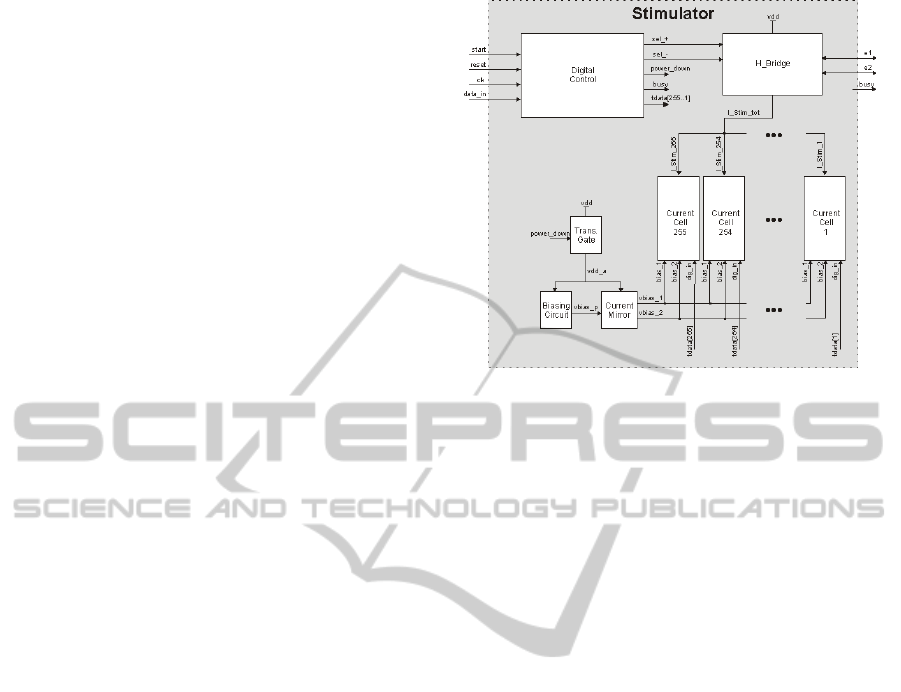
The structure of the circuit is shown in Figure 1. The
information is first received in digital form through
the serial port data_in. By using a serial interface it
is possible to save silicon area, because IO pads
require relatively large areas of silicon.
The “Digital Control” module has internal memory
to store the setup configuration, once the digital
module is programmed, it is used as a controller of
the analog stage. The module has a data bus output
Figure 1: Block diagram of the stimulator circuit.
to send information to the DAC which is composed
of 255 “Current Cells” which are responsible for
converting the digital data into an analog current
signal. The 8 bit DAC is able to source up to 256
different current values; it also has a power_down
line to put the “Voltage Bias” circuit in standby
mode in order to save power; there is also an
“H_Bridge” circuit which enables the bipolar output
by inverting the polarization of the output lines, and
makes it possible to isolate the output pins of the
output stage for performing other tasks, such as
biosignal acquisition. The stimulator behaves like a
9 bits DAC, because it allows up to 256 levels of
positive current and 256 levels of negative current.
The desired signal at the output is a current
signal. Therefore, the chosen architecture for the
DAC is current steering, since such structures
perform the conversion directly from digital to
analog current signal without a voltage stage. Thus
the design is simpler with less conversion stages and
lower power consumption.
Such an architecture is composed of several
current cells, all of them connected to a common
node in order to sum the current that each cell
drives. The binary weighted array is usually
preferable for the current cells, because of its
simplicity and reduction in the digital control logic.
But with this structure is difficult to achieve good
linearity. In an N-bit array, only N current sources
are available with variable sizes of bit current. This
can lead to a large Differential Nonlinearity (DNL)
error and an increased dynamic error during major
code transitions. When the new code signal value
appears before or after the signal value of the
previous code disappears, a glitch is seen. This
phenomenon is due to the magnitude of a glitch
BIODEVICES 2012 - International Conference on Biomedical Electronics and Devices
180
which is proportional to the number of switches that
are actually switching, The biggest glitches tend to
occur at major code transitions which is the point
where the MSB changes from low to high and all
other bits change from high to low, and vice versa.
In this case the current source for the MSB should to
be 2
N-1
times bigger than the LSB current source, it
means, the MSB represents 2
N-1
times more switches
than the LSB.
These problems are reduced by implementing the
unary array (thermometer decoded), which is formed
by 2
N
-1 current cells, each of them equally sized.
The binary input code shall be converted to a
thermometer code that turns the corresponding
current sources off or on. Some of the disadvantages
of a thermometer code array are the area and
complexity, since for each cell is required a current
source, a switch, and a decoding circuit. However,
there are advantages for a thermometer coded DAC
versus the binary type, since each level step is
created by switching only a small current cell, even
for the major transition at the binary input code.
Then the DNL error and glitch problems are greatly
reduced.
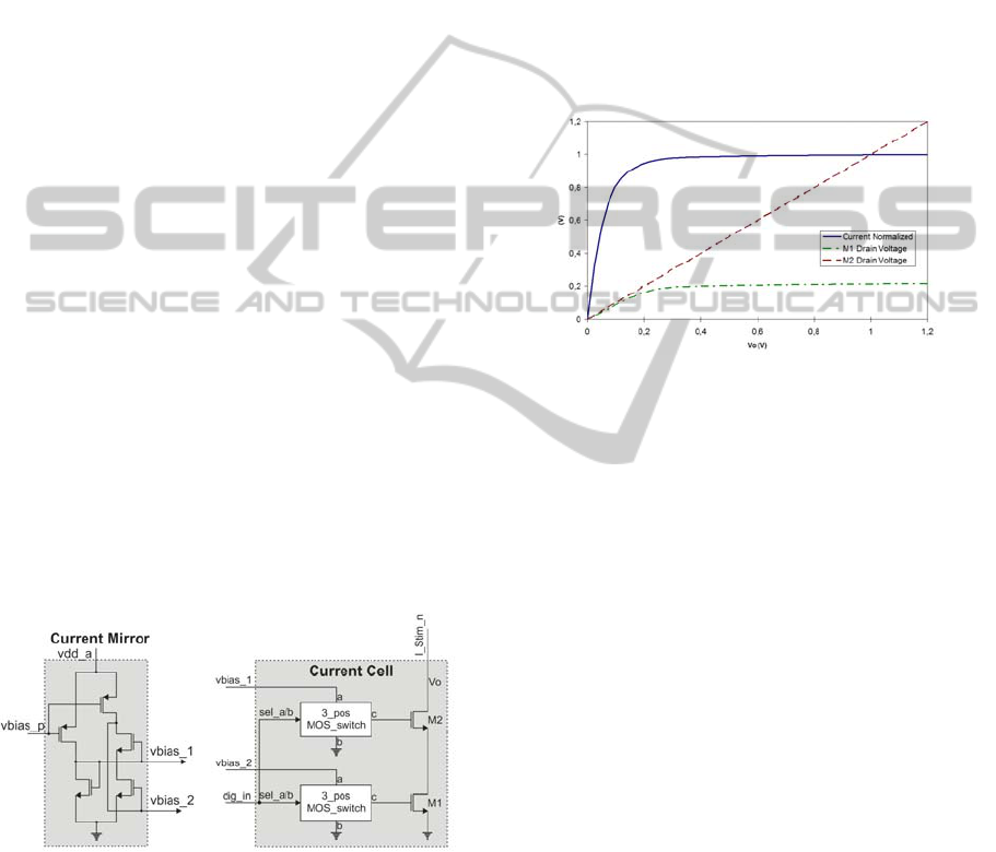
The current sources that drive the output current
shall present a large output resistance in order to be
able to drive higher load resistances and also to
present higher voltage dynamic range. This could be
achieved by implementing a current cell formed by a
cascode with NMOS transistors as illustrated in
Figure 2. It is important to bias both M1 and M2 in
saturation and to hold the drain source voltage of M1
constant in order to improve the linearity and
increase the current mirror’s output resistance.
Figure 2: Current mirror and current cell.
By biasing the cascode structure with a current
mirror as shown, it is possible to bring the drain of
M2, Vo, to the minimum possible voltage that keeps
M1/M2 in saturation, this voltage is 2V
DS,sat
; The
name of this structure is Wide-Swing Cascode. Here
the gate voltage of M1 will be V
DS,sat
+ V
THN
while
the gate voltage of M2 will be 2V
DS,sat
+ V
THN
and
their drain voltages could be V
DS,sat
and more or
equal than 2V
DS,sat
, respectively.
Figure 3 is a simulation of the cascode structure
where a voltage source was connected at the node
Vo, and the voltage was swept from 0 to 1.2 V. The
current was normalized to 1. There it is shown that
I_stim remains almost flat from 1.2 V to 250 mV
where M2 start to triodes, and then the curve
decreases slowly until 120 mV, from this point the
current decreases drastically. The voltage curves
show how the drain voltage of M1 remains stable,
allowing to keep constant the output current.
Through this simulation it can be see that this circuit
could be useful for driving current signals with a
maximum voltage around 1.1 V.
Figure 3: Simulation of the cascode structure versus a
sweep voltage.
Another advantage of these structures is the low
power consumption because the current is flowing
through the branch only when the current cell is
turned on, and this current is the same that flows
through the load.
The switches that interrupt the current’s flow are
located normally between the load and the current
cell, we chose to put them at the transistor gates in
order to minimize the number of transistors in the
branch to avoid voltage drops.
In order to keep the bias voltage stable versus
changes of voltage from power supply or
temperature, we implemented the Beta-multiplier
circuit from (Baker 2005, p. 629).
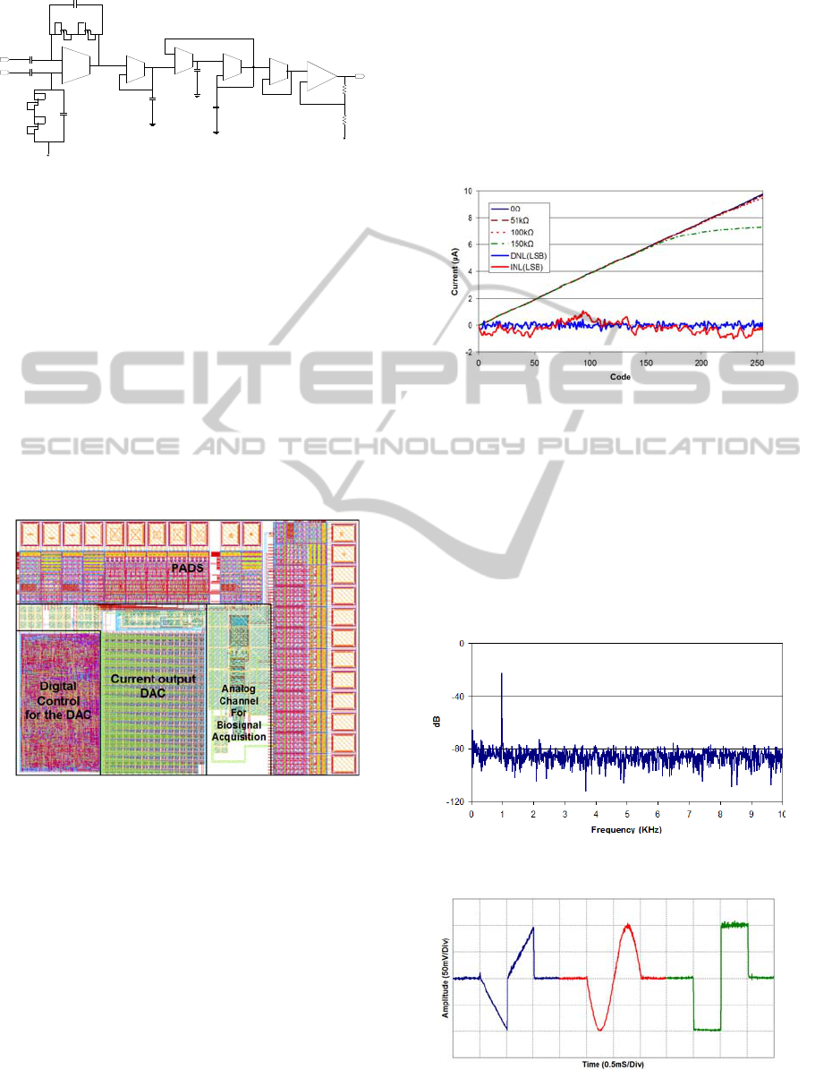
2.2 Analog Channel for Biosignal
The analog channel is used to amplify the bio-
signals at its input. It delivers an amplified analog
signal at the output. Figure 4 shows the modules of
the channel which are: Operational
Transconductance Amplifier (OTA), used at the
input. The OTA is ac-coupled in order to cancel dc-
offset of the input signal; Third order analog low-
pass filter made out of three OTAs; An OTA in
order to drive the next component; A Rail-to-Rail
post amplifier.
TOWARD THE OPTIMAL ARCHITECTURE OF AN ASIC FOR NEUROSTIMULATION
181
+
-
+
-
-
+
VGND
DRV
OTA
-
+
LP
_
OTA
LP
_
OTA
PRE
OTA
MillerC
-
+
LP
_
OTA
+
-
VGND
OUTPUT
INP-
INP+
POST
AMP
Figure 4: Structure of the analog channel for biosignal
acquisition.
3 EXPERIMENTAL RESULTS
The Figure 5 shows the layout of the fabricated
ASIC, where each module is identified. The ASIC
was fabricated in the CMOS 130 nm / 1.2 V process.
The design of the analog stage was done at transistor
level and the digital control was designed in Very
high speed integrated circuit Hardware Description
Language (VHDL) and synthesized. The dimensions
of the ASIC are 0.96 mm x 0.725 mm, the total area
is 0.696 mm
2
.
The circuit is supplied with 1.2 V for
the core and 3.3 V for the digital pads.
Figure 5: Floorplan of the ASIC.
3.1 Stimulator
The area for the stimulator is 0.257 mm
2
, from
which 0.095 mm
2
is occupied by the digital control,
0.146 mm
2
by the DAC including the current cells
and the h-bridge and 0.016 mm
2
by the voltage
biasing circuit. By setting a stimulator clock of 125
kHz, an output sinusoidal signal of 976 Hz at
maximum amplitude, the power consumption of the
stimulator was found to be 22.93 µW in standby
mode, 120.83 µW in stimulating mode without load
resistor and 128.12 µW with a 10 kΩ load.
Simulations showed the power consumption for the
“Voltage Bias Circuit” to be around 80 µW.
The transfer function for the positive pulse with
different load resistors is represented in Figure 6.
The maximum output current is ±9.8 µA, for loads
requiring less than the maximum voltage swing,
±1.097 V, the negative pulse (not shown) presents a
mismatch around 0.3%. There, it is also possible to
see the DNL and INL, its average is 0.13 and 0.40
LSB, respectively, with maximum values of 0.47
and 1.05 LSB.
Figure 6: Transfer function of the stimulator for positive
output with different load resistors and its DNL and INL.
Figure 7 shows the Fast Fourier Transform (FFT)
for the same setup with a load resistor of 10 kΩ. The
FFT bandwidth was limited to 10 kHz, because is
the range of interest of the stimulation signals. The
spurious free dynamic range SFDR was found to be
50.2 dB, the DC level was neglected.
Three different stimulation waveforms were
injected into a 10 kΩ resistive load and their
respective voltage drops are shown in Figure 8.
Figure 7: Measurement of the SFDR through the FFT of a
sinusoidal.
Figure 8: The voltage drop across a 10kΩ resistive load
for different waveforms.
BIODEVICES 2012 - International Conference on Biomedical Electronics and Devices
182
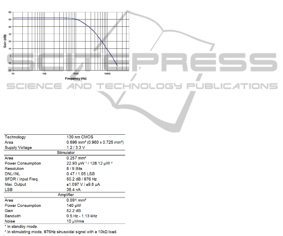
3.2 Analog Channel
The area of the analog input channel is 0.091 mm
2
,
its power consumption was found to be 140 µW.
Using a signal analyzer, with an output level of 1
mV, and a frequency range from 10 Hz to 21 kHz,
the gain for the whole channel was found to be 52.2
dB, as shown in Figure 9. The upper value of its
bandwidth was measured at 1.13 kHz, and through
simulations the lower value was found at 0.5 Hz.
The output noise level measured is 10 µV
rms
.
Figure 9: Transfer curve of the analog channel.
Table 1 summarizes results and specifications of the
ASIC.
Table 1: Measured specifications of the ASIC.
4 DISCUSSION
During stimulation, approximately 62% of the power
is consumed by the “Voltage Bias Circuit”. Thus,
the DAC architecture presented could be used in an
array of several DAC´s having only one “Voltage
Bias Circuit” and even only one “Digital Control
Unit” without a significant increase to the overall
power consumption. The same principle applies for
saving silicon area, the actual area occupied by the
pads is around 50% of the total area; the DAC itself
occupies 21%, thus it could be possible to add more
than one DAC by sharing the modules such “Voltage
Bias Circuit” and by using the same number of pads
to program the circuit in a serial way.
According to simulations performed by McIntyre
(2000), the maximum current output of 9.8 µA is
enough to activate motorneurons around 100 µm far
away from the electrode. This current could be
injected, for example, in Iridium Oxide electrodes
with a diameter of 15 µm, which present an
impedance of 113.6 kΩ (Wils, et al., 2009), or even
in smaller electrodes coated with PEDOT, in order
to increase the selectivity of the stimulation. In case
of Electrical Muscle Stimulation (EMS), or other
applications requiring higher currents and voltages,
an output amplifier could be attached, which could
be implemented in High-Voltage-Laterally-
Diffused-Metal-Oxide-Semiconductor (HVLDMOS)
process, by using such transistors with 250nm
technology it is possible to drive up to 80 V. Due to
power consumption issues it is a better option to
implement the stimulator in low voltage process and
to attach a high voltage amplifier, than implement
the whole system in a high voltage process, as was
shown by Ethier and Sawan (2010).
It is possible to migrate the design to high
voltage transistors of the same technology, its
breakdown voltage is 5 V. Thus, it is possible to
supply the system with 3.3 V. Other concerns will be
to decrease the required silicon area, to simplify the
digital control and to reduce the complexity of the
layout because of the amount of connections for
controlling the unary array.
A hybrid architecture of the current steering
DAC could overcome the negative aspects of the
unary array and binary weight array. Since binary
array DACs have problems associated with the
MSB, it is suitable to be used on the LSB side of the
DAC to handle the first few bits. For higher order
bits a unary array can be used because this
architecture can reduce the glitch effect introduced
due to MSB switching. Thus, it could be possible to
design a smaller stimulator because of the reduction
of number of current cells, and also to increase the
maximal current because of the operation voltage of
the transistors.
5 CONCLUSIONS
A system for stimulating neurons and for biosignal
acquisition was developed and fabricated. This
TOWARD THE OPTIMAL ARCHITECTURE OF AN ASIC FOR NEUROSTIMULATION
183

system offers several ways for stimulating nerve
cells. The simultaneous acquisition of biosignals
makes it possible to monitor the reactions after
stimulating.
The presented ASIC can be used for
experimental purposes, besides, the architecture of
its individual stages could be used for the design of a
neurostimulator for an specific application with an
array of several stimulators and biosignal amplifiers.
The design shows low power consumption and a
small silicon area.
REFERENCES
Ba, A. and Sawan, M., 2003. Integrated programmable
neurostimulator to recuperate the bladder functions,
IEEE ccece, vol. 1, pp. 147.
Baker, R. Jacob, 2005. CMOS Circuit Dsegin, Layout and
Simulation, Wiley-Interscience.
Barolat, G. and Sharan, A. D., 2004. Spinal Cord
Stimulation for Chronic Pain Magement, Seminars in
Neurosurgery, vol. 15, pp 151-175.
Bennie, Scott D., et al., 2002. Toward the optimal
waveform for electrical stimulation of human muscle,
Eur. J. Appl Physiol, vol. 88, pp. 13-19.
Dobelle, WM. H., 2000. Artificial Vision for the Blind by
Connecting a Television Camera to the Visual Cortex,
ASAIO Journal, vol. 46, pp.3-9.
Ethier, Sébastien and Sawan, Mohamad, 2010.
Exponential Current Pulse Generation for Efficient
Very High-Impedance Multisite Stimulation, IEEE
TBCAS, vol. 5, pp. 30-38.
Garcia Blanco, A., Jiménez, G. and Ochoa Moreno P.,
2007. Development of a Functional Neuromuscular
Stimulation System for Independent Ambulation of
Patients with a Spinal Cord Injury, Engineering
Letters.
Graf, Heinz-Gerd, et al., 2008. High Dynamic Range
CMOS Imager Technologies for Biomedical
Applications, IEEE JSSC.
Grill, Warren M. and Mortimer, J. Thomas, 1995.
Stimulus Waveforms for Selective Neural Stimulation,
IEEE EMBS.
Haddad, S. A. P., Houben, R. P. M. and Serdijn, W. A.,
2006. The Evolution of Pacemakers, IEEE Eng. Med.
Biol. Mag.
Halpern, Mark Edward, 2009. Current Waveforms for
Neural Stimulation-Charge Delivery With Reduced
Maximum Electrode Voltage, IEEE TBME, vol. 57(9).
Jezernik, S. and Sinkjaer, T., 2005. Finite Element
Modeling Validation of Energy-Optimal Electrical
Stimulation Waveform, IFESS.
Lin, Vernon and Hsiao, Ian N., 2008. Functional
Neuromuscular Stimulation of the Respiratory
Muscles for Patients With Spinal Cord Injury, IEEE,
vol. 96(7).
Mandrile, Francesco, et al., 2003. Stimulation Artifact in
Surface EMG Signal: Effect of the Stimulation
Waveform, Detection System, and Current Amplitude
Using Hybrid Stimulation Technique, IEEE TNSRE,
vol. 11(4).
McIntyre, Cameron C. and Grill, Warren M., 2000.
Selective Microstimulation of Central Nervous System
Neurons, Annals of Biomedical Engineering, vol 28,
pp. 219-233.
McIntyre, Cameron C. and Grill, Warren M., 2002.
Extracellular Stimulation of Central Neurons:
Influence of Stimulus Waveform and Frequency on
Neuronal Output, J. Neurophysiol, vol. 88, pp 1592-
1604.
Milby, A. H., Halpern, C. H. and Baltuch G. H., 2009.
Vagus Nerve Stimulation in the Treatment of
Refractory Epilepsy, Neurotherapeut., vol. 6, no. 2,
pp. 228–237.
Peckham, P. Hunter, 1981. Functional Neuromuscular
Stimulation, Phys. Technol., vol. 12.
Pezaris, John S. and Reid, R. Clay, 2007. Demonstration
of artificial visual percepts generated through thalamic
microstimulation, PNAS, vol. 104(18), pp. 7670-7675.
Pohlmeyer, Eric A., et al., 2009. Toward the Restoration
of Hand Use to a Paralyzed Monkey: Brain-Controlled
Functional Electrical Stimulation of Forearm Muscles,
PLOS ONE, vol. 4(6).
Ring, Haim and Rosenthal, Nechama, 2005. Controlled
Study of Neuroprosthetic Functional Electrical
Stimulation in Sub-Acute Post-Stroke Rehabilitation,
J. Rehabil. Med, vol. 37, pp. 32-36.
Robillard, Charles, et al., 2006. Neural stimulation safety
and energy efficiency: Waveform analysis and
validation, IFESS.
Rubinstein, Jay T., 2004. How cochlear implants encode
speech, Current Opinion in Otolaryngology & head
and Neck Surgery, vol. 12, pp. 444-448.
Rush, A. J., et al., 2000. Vagus Nerve Stimulation (VNS)
for Treatment-Resistant Depressions: A Multicenter
Study, Biol Psychiatry, vol. 47, pp 276–286.
Sahin, Mesut and Tie, Yanmei, 2007. Non-rectangular
waveforms for neural stimulation with practical
electrodes, J. Neural Eng., vol. 4, pp. 227-233.
Veraart, C., et al., 2003. Pattern Recognition with the
Optic Nerve Visual Prosthesis, Artif. Organs., vol.
27(11).
Wils, Seth J., et al., 2009. Poly(3,4-
ethylenedioxythiophene) as a micro-neural interface
material for electrostimulation, Frontiers in
Neuroengineering, vol. 2.
BIODEVICES 2012 - International Conference on Biomedical Electronics and Devices
184
