
Ablation of (Ges
2
)
0.3
(Sb
2
S
3
)
0.7
Employing Nanosecond UV Laser
Petr Knotek
1, 3
, Jakub Navesnik
1
, Milan Vlcek
2, 3
and Ladislav Tichy
2, 3
1
University of Pardubice, Faculty of Chemical Technology, Studentska 573, 532 10 Pardubice, Czech Republic
2
Institute of Macromolecular Chemistry, AS CR, Heyrovskeho sq. 2, 162 06 Prague, Czech Republic
3
Present address: Joint Laboratory of Solid State Chemistry of Institute of Macromolecular Chemistry Academy of Sciences
of Czech Republic, v.v.i., and University of Pardubice, Studentska 84, 532 10 Pardubice, Czech Republic
Keywords: Chalcogenide Glass, Ablation, UV Nanosecond Laser, Microlens.
Abstract: The interaction of (GeS
2
)
0.3
(Sb
2
S
3
)
0.7
glass and UV nanosecond laser has been described. The material was
ablated and the dependencies of the most important parameters as number and energy of the pulses and
repetition rate to the volume of the craters were correlated.
1 INTRODUCTION
Laser based fabrication technologies are widely used
to prepare: thin films (PLD (Frumar et al., 2006)),
optical waveguide (Bryce et al., 2004), convex or
concave microlenses and microlens arrays (Lim et
al., 2006); (Fritze et al., 1998) as the passive optical
elements. The patterns are formed by the focusing
laser energy in order to process materials at the
microstructure (Hitz et al., 2012). Different types of
laser operation (continuous or pulsed modes) enable
to use proper combination of laser experimental set-
up to studied material and demanding process. The
absorption of photons can lead to excitation of
electrons in target materials. If the energy is high
enough, the energy transfer leads to the material
release by thermal vaporization or by photochemical
interactions (Hitz et al., 2012); (Knotek et al., 2012).
The influence of ultraviolet light (UVL) to the
certain optical and physical behavior of the
chalcogenide glasses and films has been previously
studied. There were described the classical photo-
induced effects as photo-darkening, photo-expansion
and decrease of the refractive index (Bryce et al.,
2004); (Messaddeq et al., 2001); (Marquez et al.,
2009). The unique changes of behavior were
accounted to the photo-induced structural changes in
an amorphous state, reaction with surroundings as
photo-oxidation or crystallization of the material
(Messaddeq et al., 2001), (Bryce et al., 2004).
In this communication we focused on the
interaction of UV pulsed laser with the bulk glassy
(GeS
2
)
0.3
(Sb
2
S
3
)
0.7
material. Ge-Sb-S system, mainly
(GeS
2
)
x
(Sb
2
S
3
)
1-x
stoichiometric system, renewed
attractiveness (Fatome et al., 2009); (Lin et al.,
2012) for a high stability to the humid air, high
linear and non-linear values of the refractive index
and high glass forming and crystallization
temperatures. We selected this chemical
composition as chemically (stoichiometric system)
and mechanically stable system (mean coordination
number of the glass (CN=2.45) is close to the
threshold value according Phillips model (Phillips,
1979)). The aim of this study was to examine
interaction of nanosecond UV laser with
(GeS
2
)
0.3
(Sb
2
S
3
)
0.7
glass and to determine some of
the most important parameters as the pulse laser
energy, the repetition rate and the number of pulses
in relation to the modification of the sample.
2 EXPERIMENTAL
The glassy (GeS
2
)
0.3
(Sb
2
S
3
)
0.7
bulk was prepared by
a direct synthesis from elements (5N purity)
according procedure described elsewhere (Knotek
and Tichy, 2012). The optically polished samples
were illuminated under the air atmosphere through 5
nsec pulsed laser operating at a wavelength 213 nm
in the laser ablation system LSX-213 G2 (CETAC,
USA) with the maximum emitted energy 4.5 mJ per
pulse.
The laser beam was focused onto the upper
surface by means of an optical microscope objective
to the spot with a diameter 25 µm. Two sets of
illuminated spots were formed for each combination
5
Knotek P., Navesnik J., Vlcek M. and Tichy L..
Ablation of (Ges2)0.3(Sb2S3)0.7 Employing Nanosecond UV Laser.
DOI: 10.5220/0004312300050009
In Proceedings of the International Conference on Photonics, Optics and Laser Technology (PHOTOPTICS-2013), pages 5-9
ISBN: 978-989-8565-44-0
Copyright
c
2013 SCITEPRESS (Science and Technology Publications, Lda.)
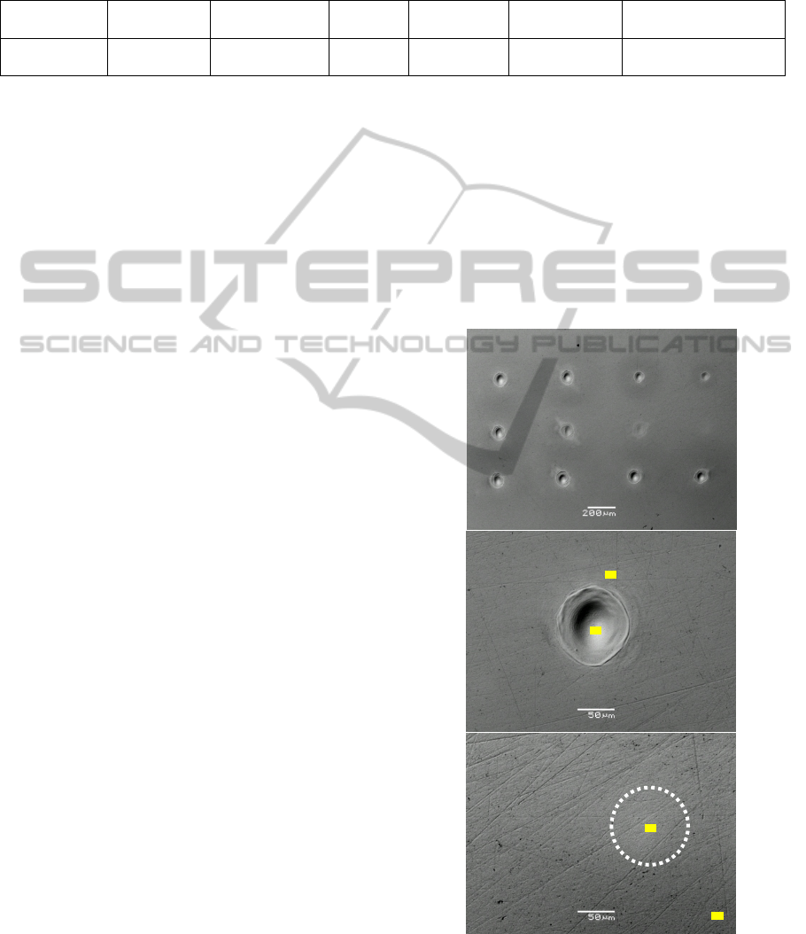
Table 1: Material characteristics of the (GeS
2
)
0.3
(Sb
2
S
3
)
0.7
glass (E
03
band gap energy, the average coordination number
(CN)) and certain parameters which characterize the conditions of illumination: the wavelength (λ
ill
and photon energy
(ħω
ph
), the pulse energy (E
pulse
), the average emitted light intensity at repetition 20 Hz (I
aver.
), the corresponding penetration
depth of the light (d
p
), the area of the light spot on the sample (A), the effective volume (V
eff
=A*d
p
), where photons are
adsorbed and the absorbed light power (P
A
) during the pulse and average value.
E
03
/CN
*
(eV/-)
λ
ill
/ħω
ph
(nm/eV)
E
p
ulse
/
I
aver.
(mJ/mW)
d
p
(nm)
A
(cm
2
)
V
eff
(cm
3
)
P
A
aver.
/ P
A
p
ulse
(W.cm
-3
)
2.11/2.45 213/5.82 4.5/90 5 4.9×10
-6
2.5×10
-12
3.7×10
10
/3.7×10
17
* CN = 4x+3y+2(1-x-y) for Ge
x
Sb
y
S
1-x-y
(Philips, 1979)
of experimental parameters.
The chemical composition was verified using
electron microprobe X-ray (EDX) analyses (Jeol
JSM 5500-LV). In order to monitor surface and
near-sub-surface states the penetration depth of
electrons was adjusted to be at around 500 nm. The
transmission was measured using a Perkin-Elmer
Lambda 12 spectrophotometer.
Measurements with a digital holographic
microscope (DHM) were realized by means of a
DHMR1000 (Lyncée Tec, Switzerland) operating at
785 nm in a reflection configuration (Knotek et al.,
2009).
3 RESULTS AND DISCUSSION
Certain material characteristics of the studied glass
and the conditions of the samples illumination are
summarized in Table 1 (see (Knotek and Tichy,
2012); (Knotek et al., 2010) for details of analysis).
The UV photon energy was highly over-band gap
energy (E
ph
=5.82 eV >>E
03
=2.11 eV) and photons
were absorbed in thin layer (d
p
= 5 nm). These
conditions resulted to the high values of absorbed
light power (P
A
pulse
= 4x10
17
W.cm
-3
) followed by a
destruction of the bonding system, photons energy
conversion to the heat with low dissipation of the
heat and vaporization of the material (Mendes,
2006).
There were tested three the most important
parameters for laser-material interaction: the pulse
laser energy (0.2 – 4.5 mJ per pulse denoted as
series 1), the number of pulses (1 – 50 pulses - series
2) and the repetition rate (1 – 20 Hz - series 3). If not
mentioned elsewhere, the typical conditions were
4.5 mJ per pulse, 20 Hz repetition rate, number of
pulses 50 and 25 µm spot diameter.
Under all mentioned conditions, there were
created craters after UV exposition of
(GeS
2
)
0.3
(Sb
2
S
3
)
0.7
as summarized in Fig. 1a. The
SEM details of craters “drilled” with the maximum
energy (4.5 mJ) and 50 pulses with the repetition
rate 20 Hz and 1 pulse with 4.5 mJ energy are
depicted in Fig. 1b and 1c, resp. All the craters were
subsequently topographically analysed employing
digital holographic microscope (DHM). The typical
line-scans across the centre of the craters are
illustrated in Fig. 2.
The diameter of the craters with maximal pulse
energy was 95 – 100 µm with the depth 3.3 µm. The
obtained craters were analyzed employing AFM
software (Klapetek et al., 2011) to determine the
Figure 1: SEM images of ablated craters a) summarizing
photo; b,c) details of the crater created by 50 pulses, 4.5
mJ per pulse, and by single 4.5 mJ pulse, resp.
centre of the crater
non illuminated
centre of the crater
serie 2
serie 1
serie 3
out of the crater
a
b
c
PHOTOPTICS2013-InternationalConferenceonPhotonics,OpticsandLaserTechnology
6
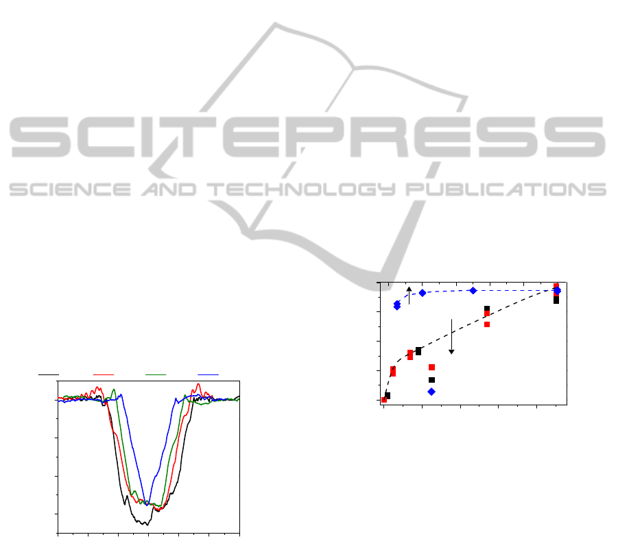
-90 -60 -30 0 30 60 90
-3000
-2000
-1000
0
Topography (nm)
X line (µm)
serie 1 - pulse energy
4.5 mJ 2.7 mJ 0.7 mJ 0.2 mJ
volume of the crater as the parameter chosen for a
crater characterization. The reproducibility of the
process was checked by analysis of the six craters
prepared under similar conditions of illumination
(50 pulses, 4.5 mJ per pulse and 20 Hz repetition).
The average volume was determined as 10 600 µm
3
with standard error less than 300 µm
3
which seems
to be reproducible values and the process.
The volume of the craters increased nonlinearly
with the increase of the counts or the pulse energy
(Fig. 3) independently on the way of supply of the
cumulative energy. The line-scans detected the
differences in the shape of the craters. If the craters
were formed by low pulse energy (0.2 mJ per pulse),
the profile is “V-shaped”, however with the higher
pulse energy (>0.6 mJ per pulse) the profile is “U-
shaped”. The craters formed with low energy pulse
(0.2 mJ) could be used as an element of the
microlens array. The curvature (R) of the circle
formed when passes through the three points (two on
the basal plane and one at a maximum of
microlenses) equals to: R = (d
2
+ r
2
)/2d =
(2.7
2
+(54/2)
2
/(2×2.7)=136 µm, where d is the depth
of the microlens and r is the radius of the basal
plane. This value seems to be well comparable to R
values for the microlens in oxide (R ≈ 150 µm) or in
chalcogenide (R ≈ 170 µm) glasses (Beadie et al.,
1998); (Huang et al., 2008); (Knotek and Tichy,
2012). The micro-scratches, as the consequence of
the polishing of the bulk material, were partly
smoothed even after single pulse (marked spot area
on Fig. 1c).
Figure 2: The line-scans of the craters of the serie 1 (the
energy of the pulses in range 4.5 – 0.2 mJ, 50 pulses -see
text).
The volume of the craters are independent on the
repetition rate in the range 5 – 20 Hz (see Fig. 3,
blue line); whereas the volume slightly decrease
(<15 %) for the lowest repetition rate (1 Hz). The
low sensitivity of the volume to the repetition rate
could by caused by the nanosecond time period for
energy of UV photons to transfer to the heat and to
vaporize the material during the pulse.
The chemical composition and its changes after
the process of illumination were tested by EDX
analysis on the areas denoted on Fig. 1 as the yellow
rectangles. From the EDX analyses we found a
constant ratio of small and rather broad K
O
line at
around 0.55 eV and L
Ge
line at around 1.2 eV (I
Ge
/I
O
≈ 3.6) for the non-illuminated sample and for the
sample illuminated for 1 pulse with P
A
pulse
=
1.6×10
16
W.cm
-3
. Hence we suppose that within the
sensitivity of EDX analyses there is practically no
serious indication of photo-oxidation. We believe
that this is an acceptable result because from kinetics
limits photo-oxidation requires a time > 5 nsec even
for the photons with an energy above 5 eV. On the
other hand, the partial oxidation is evident in EDX
comparing the centre of the crater and the deposit
after ablation near the crater formed by 50 pulses
(for location see Fig 1b) with non-illuminated glassy
bulk as an increase of the broad O band near 0.55 eV
(I
Ge
/I
O
= 2.6 and 2.1 for the crater center and the
deposit out of the crater, resp.).
048121620
0 50 100 150 200
0
3000
6000
9000
12000
Repetition rate (Hz)
V
crater
(µm
3
)
Cumulative energy (mJ)
serie 1 - pulse energy
serie 2 - pulse number
serie 3 - repetition
Figure 3: The dependences of the crater volume on the
experimental conditions.
As mentioned in Introduction, the UV photo-
induced expansion of the material is described in the
literature. In present experiments the “gentle”
exposition condition was realized by increasing of
the diameter of the illuminated spot to the 200 µm
and minimal pulse energy 0.2 mJ (P
A
pulse
= 2.5×10
14
W.cm
-3
). The material was still ablated after 5 pulses
even under the low energy conditions (0.2 mJ)
however the single pulse led to the elevation of the
material (Fig. 5). Observed expansion of the material
by 50 nm had to be connected with thermal-effect.
UV photons can penetrate less than 5 nm which is
Ablationof(Ges2)0.3(Sb2S3)0.7EmployingNanosecondUVLaser
7
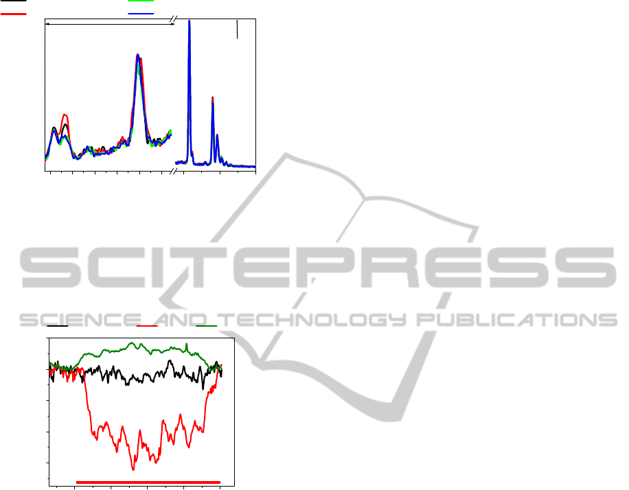
-100 -50 0 50 100
-300
-200
-100
0
100
spot 200 µm
Topography (nm)
X line (µm)
non illuminated 5 pulses 1 pulse
0,4 0,6 0,8 1,0 1,2 1,4 2 4 6
1
pu
l
se
centre of the crater
non illuminated
200 counts
Sb
Sb
Sb
Sb
Sb
S
S
intenzity x5
Ge
O
Sb
EDX signal
E
(
keV
)
50
pu
l
ses
centre of the crater
out of the crater
Figure 4: The EDX spectra of the samples, for location of
analysis see Fig. 1 and the text.
too small depth to expand the material by 50 nm.
Hence the heat should be dissipated deeper into the
bulk.
Figure 5: The line-scans of non-illuminated material,
material after 5 and single pulse (200 µm diameter of the
spot, pulse energy 0.2 mJ)
4 CONCLUSIONS
- The interaction of the 213 nm UV nanosecond
laser with chalcogenide glass (GeS
2
)
0.3
(Sb
2
S
3
)
0.7
has
been described;
- Influence of the most important parameters as
energy of the pulse, number of pulses and repetition
rate on the volume of the craters has been described;
- The shape of the craters is dependent on the
condition of illumination and at low energy pulses
created craters could be used for formation of
microlens array;
- Future work will be focused on the structural
changes of the material and analysis of the ablated
material.
ACKNOWLEDGEMENTS
The authors acknowledge financial support from the
project Grant Agency of the Czech Rep. (GPP108/
12/P044). We are indebted to Dr. M. Kincl for
technical assistance.
REFERENCES
Beadie, G., Rabinovich, W. S., Sanghera, J. & Aggarwal,
I. 1998. Fabrication of microlenses in bulk
chalcogenide glass. Opt. Commun., 152, 215-220.
Bryce, R. M., Nguyen, H. T., Nakeeran, et al. 2004. Direct
UV patterning of waveguide devices in As
2
Se
3
thin
films. J. Vac. Sci. Technol. A, 22, 1044-1047.
Fritze, M., Stern, M. B. & Wyatt, P. W. 1998. Laser-
fabricated glass microlens arrays. Opt. Let., 23, 141-
143.
Frumar, M., Frumarova, B., Nemec, P., Wagner, T.,
Jedelsky, J. & Hrdlicka, M. 2006. Thin chalcogenide
films prepared by pulsed laser deposition - new
amorphous materials applicable in optoelectronics and
chemical sensors. J. Non-Cryst. Solids, 352, 544-561.
Hitz, B., Ewing, J. & Hecht, J. 2012. Introduction to Laser
Technology, New York (USA), Wiley-IEEE Press.
Huang, Y., Liu, R., Lai, J. J. & Yi, X. J. 2008. Design and
fabrication of a negative microlens array. Opt. Laser
Technol., 40, 1047-1050.
Klapetek, P., Nečas, D. & Anderson, C. 2011. Gwyddion -
Free SPM data analysis software; v. 2.25.
Knotek, P., Arsova, D., Vateva, E. & Tichy, L. 2009.
Photo-expansion in Ge-As-S amorphous film
monitored by digital holographic microscopy and
atomic force microscopy. J. Optoelectron. Adv. M., 11,
391-394.
Knotek, P., Kincl, M., Tichy, L., Arsova, D., Ivanova, Z.
G. & Ticha, H. 2010. Oxygen assisted photoinduced
changes in Ge
39
Ga
2
S
59
amorphous thin film. J. Non-
Cryst. Solids, 356, 2850-2857.
Knotek, P. & Tichy, L. 2012 On photo-expansion and
microlens formation in (GeS
2
)
0.74
(Sb
2
S
3
)
0.26
chalcogenide glass. Mater. Res. Bull., 47, 4246-4251.
Knotek, P., Vlcek, M., Kincl, M. & Tichy, L. 2012. On the
ultraviolet light induced oxidation of amorphous As
2
S
3
film. Thin Solid Films, 520, 5472-5478.
Lim, C. S., Hong, M. H., Kumar, A. S., Rahman, M. &
Liu, X. D. 2006. Fabrication of concave micro lens
array using laser patterning and isotropic etching. Int.
J. Mach. Tool Manu., 46, 552-558.
Lin, C. G., Li, Z. B., Ying, L., Xu, Y. S., Zhang, P. Q.,
Dai, S. X., Xu, T. F. & Nie, Q. H. 2012. Network
Structure in GeS
2
-Sb
2
S
3
Chalcogenide Glasses: Raman
Spectroscopy and Phase Transformation Study. J.
Phys. Chem. C, 116, 5862-5867.
PHOTOPTICS2013-InternationalConferenceonPhotonics,OpticsandLaserTechnology
8

Marquez, E., Jimenez-Garay, R. & Gonzalez-Leal, J. M.
2009. Light-induced changes in the structure and
optical dispersion and absorption of amorphous
As
40
S
20
Se
40
thin films. Mater. Chem. Phys., 115, 751-
756.
Mendes, M. 2006. Semiconductor applications using
short-pulsed UV lasers. Solid State Technol., 49, 42-
46.
Messaddeq, S. H., Siu LI, M., Lezal, D., Ribeiro, S. J. L.
& Messaddeq, Y. 2001. Above bandgap induced
photoexpansion and photobleaching in Ga-Ge-S based
glasses. J. Non-Cryst. Solids, 284, 282-287.
Phillips, J. C. 1979. Topology of covalent non-crystalline
solids 1- short-range order in chalcogenide alloys. J.
Non-Cryst. Solids, 34, 153-181.
Ablationof(Ges2)0.3(Sb2S3)0.7EmployingNanosecondUVLaser
9
