
The Characterisation and Optimisation of TLC NAND Flash Memory
using Machine Learning
A Position Paper
Sorcha Bennett and Joe Sullivan
Limerick Institute of Technology, Limerick, Ireland
K
eywords:
Non-volatile Memory, Flash Memory, Reliability, Endurance, Retention, Wearout, NOR, NAND, Multi-Level
Cell (MLC), Triple-Level Cell (TLC), Machine Learning (ML).
Abstract:
Flash memory is non-volatile and, while it is becoming ever more commonplace, it is not yet a complete
replacement for hard disk drives. The physical layout of Flash means that it is more susceptible to degradation
over time, leading to a limited lifetime of use. This paper will give an introduction to NAND Flash memory,
followed by an overview of the relevant research on the reliability of MLC memory, conducted using Machine
Learning (ML). The results obtained will then be used to characterise and optimise the reliability of TLC
memory.
1 INTRODUCTION
Up until relatively recently spinning hard disk drives
were the most common, permanent, form of data stor-
age. However, this space is now being rapidly filled
by NAND Flash memory,with Flash taking more than
two-thirds of the total non-volatile silicon memory
market (KonceptAnalytics, 2010).
Flash memory is a non-volatile memory, meaning
that it does not lose data when the power source is
removed. It has a complex memory cell structure,
which can be erased by electrical methods (Pavan
et al., 1997). It was called Flash because the data
could be erased very quickly - in a flash (Aritome
et al., 1993).
Important reliability metrics with regards to Flash
memory are endurance and retention. Endurance is
a measure of how many program/erase (P/E) cycles
a cell can endure before failure (IEEE, 1998). The
endurance values vary between device types and also
between manufacturers. Common values for Single
Level Cell (SLC) can be 100,000, for MLC can be
5,000-10,000, while for TLC it can be as little as 500
P/E cycles.
Retention is a measure of how long a device can
retain settings without being refreshed. According
to the JEDEC specification (JEDEC, 2011) for Flash,
these figures should be 1 year for 100% of the maxi-
mum cycle count, and 10 years for 10% of the max-
imum cycle count. This means that if a Flash device
is cycled to 100% of it’s maximum P/E cycle count,
then it has to keep the data for 1 year, and if it’s cycled
at only 10%, then it has to keep the data for 10 years.
P/E cycling creates significant endurance and re-
tention problems which cause the eventual wearout of
all Flash memory devices (Pavan et al., 1997). The
physics of Flash mean that the electrical stress as-
sociated with changing state are the most common
cause of threshold voltage (V
th
) disturbances (Com-
pagnoni et al., 2010). The V
th
of a cell is the gate
voltage at which it is turned on, and disturbances can
occur due to degradation in the tunnel oxide. Sev-
eral methods are employed to combat this wearout
mechanism, including Wear Leveling and Error Cor-
rection Codes (ECCs), all of which are carried out by
the Flash memory controller. This controller creates
a single error free data stream from multiple NAND
devices and hides the complexity of doing so from the
user. It is typically comprised of a host interface and
a Flash File System (FFS).
Wear Leveling is required because, without it,
data may be continually updated in the same loca-
tion, leaving other locations less-frequently updated,
or not used at all. This can lead to specific, frequently
updated blocks wearing out prematurely. To prevent
this, the usage of all pages must be kept as level as
possible. ECCs are used to correct read errors and are
executed from the spare area of the memory. There
are many types of ECC, but the most well-known are
Reed-Solomon and Bose & Ray-Chaudhuri (BCH)
559
Bennett S. and Sullivan J..
The Characterisation and Optimisation of TLC NAND Flash Memory using Machine Learning - A Position Paper.
DOI: 10.5220/0004330305590564
In Proceedings of the 5th International Conference on Agents and Artificial Intelligence (ICAART-2013), pages 559-564
ISBN: 978-989-8565-39-6
Copyright
c
2013 SCITEPRESS (Science and Technology Publications, Lda.)
(Micheloni et al., 1998). ECCs are needed to deal
with various issues including noise, V
th
disturbances,
retention, and related errors, while performing read
operations. They are used to increase both endurance
and retention of the Flash.
This research will focus on characterising and
quantifying the reliability of TLC NAND Flash, and
is being undertaken as part of wider collaborative re-
search by a group comprised of one industrial and two
educational institutions. The rest of this paper is laid
out as follows: a background to Flash memory, previ-
ous research on NOR and NAND Flash memory us-
ing ML, current research on TLC NAND Flash mem-
ory, the tool chain developed, current position, future
work, and conclusions.
2 BACKGROUND
There are two distinct types of Flash memory - NOR
and NAND. NOR provides fast random memory read
access and so, is used to store code and parameter
data, because it guarantees 100% good bits (Tewks-
bury and Brewer, 2008). Random access means the
memory can be directly addressed and data can be
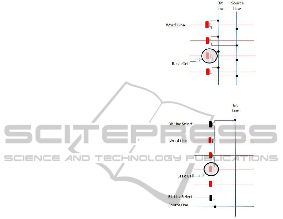
found in any order, anywhere. As shown in Figure 1,
each cell is connected to both the bit and source line,
facilitating random access. NAND is better for appli-
cations that need serial read access, whereas NOR is
better when random read access is required. NAND
does allow random access but data access is slower
than NOR (Tewksbury and Brewer, 2008). Random
write has been shown to be as fast on raw NAND
Flash as serial write access, but slower on Solid State
Devices (SSDs) (Desnoyers, 2010).
Serial access facilitates data extraction by pass-
ing the data through the rest of the cells in the string,
which are put into pass mode, by turning all the cells
on. This allows access to the required cell. All cells
on a Word Line must be read together and form a
page of data, as shown in Figure 2. This diagram
shows that each bit line is shared by a string of cells,
therefore allowing serial access. NAND is denser and
cheaper than NOR, so has taken over for use in data
storage, memory cards, mobile phones and SSDs -
where the cost per bit is critical. This fact, along with
increased demand for smaller devices, has caused the
NAND Flash market to grow to over $25 billion in
2011(Lee, 2011).
Both NOR and NAND are based on a Floating
Gate (FG) technology consisting of a MOS (Metal
Oxide Silicon) Field Effect Transistor or MOSFET.
The MOS structure has three layers - the Metal layer
is the control gate, the Oxide layer holds the floating
Figure 1: NOR Flash Architecture.
Figure 2: NAND Flash Architecture.
gate, and the Silicon layer.
The floating gate is isolated from the silicon layer
by the oxide layer surrounding it. The electrons are
tunneled through this oxide layer, as shown in Fig-
ure 3. Once a charge is added to the floating gate
by a programming operation, it is permanently stored
there until an erase operation is performed (Bez et al.,
2003) (Hasler and Lande, 2001). The effect of these
program and erase operations is to change the V
th
of
the cell.
NOR is programmed by channel-hot-electron
(CHE) injection and erased by Fowler-Nordheim
(FN) tunneling (Bez et al., 2003). Programming
by CHE involves accelerating electrons through the
channel between source and drain. These electrons
have enough energy to get over the oxide barrier and
into the floating gate. Erasing by FN involves apply-
ing a high negative voltage to the cell gate with re-
spect to the substrate. This results in the electrons
being pulled from the floating gate into the substrate.
NAND memory uses FN tunneling for programming
and erasing. Programming involves applying a high
ICAART2013-InternationalConferenceonAgentsandArtificialIntelligence
560
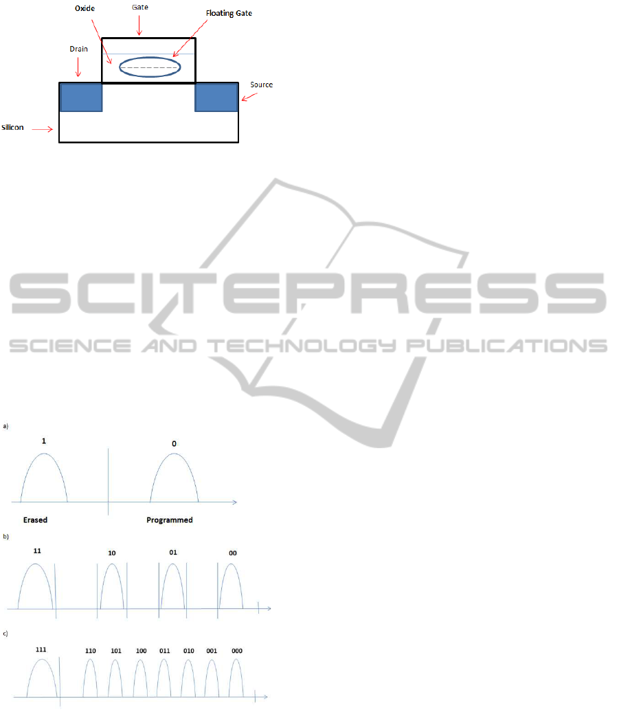
Figure 3: Floating Gate.
positive voltage to the cell gate with respect to the
substrate. The electrons are then pulled from the sub-
strate into the floating gate.
Within the NAND Flash family, there are three
distinct types of memory. SLC can store only 1 bit
of data per cell, and can be either programmed (0) or
erased (1), as shown in Figure 4 (a). MLC stores 2 bits
of data per cell in 4 levels - 00 Fully Programmed, 01
Partially Programmed, 10 Partially Erased, 11 Fully
Erased, as detailed in Figure 4 (b).
Finally, TLC stores 3 bits of data per cell in 8 lev-
els, ranging from 000 Fully Programmed to 111 Fully
Erased. The assumed V
th
distribution arrangements
are shown in Figure 4 (c).
Figure 4: Voltage Threshold Distribution for SLC, MLC
and TLC.
3 PREVIOUS RESEARCH
Machine Learning algorithms are algorithms which
improve through experience, by evolving behaviours
based on empirical data. This research group is us-
ing a family of these algorithms called Evolutionary
Algorithms, and two branches in particular - Genetic
Algorithms (GAs) and Genetic Programming (GP).
These are used for search and optimisation problems.
Both techniques are similar, the primary difference
being how potential solutions are represented. GA
solutions are represented as bit strings, whereas GP
solutions are represented as tree structures.
The earliest work on Flash endurance using ML
was conducted on NOR memory (Sullivan and Ryan,
2007). In this study, GAs were applied in real time
to chips in order to find out if the endurance of Flash
memory could be improved by evolving a better set
of control parameters. A control group was created
by testing a group of cells using factory default val-
ues. A single device was used for each run, compris-
ing 7 generations. This work proved that endurance
could be extended by up to 3.5 times that of the con-
trol group.
A recent discovery (Desnoyers, 2010) found that
the latency of read, program and erase operations was
lower than the values specified by the manufacturers.
Furthermore, due to degradation of the oxide after
use, programming speed increased and erase speed
decreased. Similar results on programming speed
were found by this research groupduring work carried
to characterise NAND. However, it was found that
erase time initially decreased sharply, levelled out,
then increased. A theory was put forth that this ini-
tial decrease was the by-product of an erase algorithm
performed on the chip itself. This algorithm would
operate similarly to Incremental Step Pulse Program-
ming (ISPP) (Suh et al., 1995), in that a series of erase
pulses would be performed to make up an erase oper-
ation.
A further finding during the analysis of data was a
significant difference in performance between blocks
in different locations in a plane, and between pages
in a block. Analysis of endurance across pages in
a block (Yaakobi et al., 2010) found a difference
between MSB and LSB pages. A similar analysis
(Cai et al., 2012) was performed with similar results,
with the addition of identifying 4 distinct types of
pages in each block - a Most Significant Bit (MSB)-
even and MSB-odd page, and a Least Significant Bit
(LSB)-even and LSB-odd page. Results found by
our research group were similar, but performed by
analysing all the blocks in a chip, which gave rise
to a distinct block-level pattern. Program and erase
times were analysed as a function of P/E cycles. We
concluded that by using these three values, ML would
be able to create a function capable of predicting en-
durance values for a particular block.
Further research carried out during this time fo-
TheCharacterisationandOptimisationofTLCNANDFlashMemoryusingMachineLearning-APositionPaper
561
cused on predicting end-of-lifefor a NAND Flash part
by using start-of-life measurements, such as program
and erase time (Hogan et al., 2012a). This study used
GP, an extension of GAs (Koza, 1992), to evolve a
mathematical function that, given the start-of-life val-
ues for read, write and erase times, would predict the
useful life of the NAND Flash block. The model ob-
tained up to 95% accuracy on unseen data, thereby
proving that it is possible to use this implementa-
tion method to predict real endurance figures (Hogan
et al., 2012a).
A parallel study to predict retention limits of MLC
chips was also carried out using GP (Hogan et al.,
2012b). In this work an accelerated test period was
developed to test retention, as it takes too long to test
retention by waiting for the actual retention period.
This involved cycling blocks at high temperature, to
replicate normal lifetime usage, followed by a data
error count. Next, a specific hexadecimal data pat-
tern was written to the device, after which the device
was put into an environmental oven and baked at a
high temperature for a period of time. This was cal-
culated using Arrhenius’ Equation to be equivalent to
3 months at normal operating temperature. When the
bake cycle finished, the data was again read from the
device and compared with the data originally written
to it. The GP function was then evolved using the
number of cycles performed and the number of pre-
retention errors as inputs, with the output being the
number of post-retention errors. The results from this
research showed that it was possible to classify the
retention period over 85% of the time.
To date, there have been a number of similar
studies on MLC endurance. One of the most rel-
evant demonstrated firstly, that there is a large per-
formance difference between manufacturers, devices
and datasheet reliability figures. And, secondly, that
there was a difference within blocks when compar-
ing power usage, speed of operations and error rates
(Grupp et al., 2009).
4 CURRENT RESEARCH ON TLC
The theory of a TLC memory cell was proposed in
1997 (Tanaka et al., 1997). This new cell would have
a reduced capacity area and efficient ECC. In 1995, a
method of increasing the density of the NAND Flash
cells was proposed (Hemink et al., 1995), using up to
4-level cells. This would require narrow V
th
distribu-
tions and high programming speeds.
It is our contention that TLC will suffer from the
same problems with reliability as both SLC (Aritome
et al., 1993) and MLC (Grupp et al., 2009), but to
Figure 5: Research Group.
greater degrees. Instead of having two states, pro-
grammed or erased, like in SLC, or four states, like
in MLC, there are now eight possible states for TLC,
as shown in Figure 4 (c), which means there is a
far higher chance of V
th
distributions crossing read
boundaries, leading to errors. Because of this, the
differences in endurance gradients across blocks and
pages in TLC needs to be characterised and quanti-
fied.
At the time of writing, there was very little pub-
lished data or literature on TLC, especially with re-
gards to endurance and retention. This leaves a sub-
stantial gap in TLC knowledge which this research
will attempt to fill. As well as studying the relia-
bility gradient differences in TLC, a complete block
map layout of the specific TLC chips obtained for
this project will be laid out. Testing will take into
account retention and the permitted Bit Error Rate
(BER) for the device as prescribed by the size of the
spare area. Also, the method used to perform error
mapping across blocks and pages in TLC chips will
be investigated. Finally, the results of this work will
be incorporated into ML trials that will be run on
TLC chips, using the methods refined in the studies
by Hogan (Hogan et al., 2012a) and Hogan (Hogan
et al., 2012b), to optimise TLC reliability.
A recent relevant study (Yaakobi et al., 2012)
mapped the layout of a TLC block and the BER on the
level of a block, a page, and a bit, in a selection of in-
dividual blocks. This research mapped a TLC page as
ICAART2013-InternationalConferenceonAgentsandArtificialIntelligence
562
having a Left and Right MSB page, a Left and Right
Central Significant Bit (CSB), and a Left and Right
LSB. To do this, firstly a typical layout of a TLC chip
was devised. Next, the BER was analysed, both as an
average across a number of blocks, and on individual
pages in a block. It was discovered that often the state
of the cell in question changed from “the highest level
to the lowest level”, rather than one level at a time. A
theory proposed to explain this was that the three bits
in a TLC chip were not being programmedat the same
time, but instead, one at a time. This meant that if an
error occurred in either the first or second bit, the state
of the cell would be changed by more than one level.
Finally, a new ECC was designed, which would work
on all three bits simultaneously.
Reliability is a function of both endurance and re-
tention, and while the work mentioned above focused
on ECC design, it tested for endurance only, with no
attempt at retention testing. Furthermore, only a sam-
ple of blocks were trialled and so, no endurance map
applicable across devices could be drawn. The pro-
posed work will seek to expand and fill the gaps dis-
cussed, by also making use of GP, as described in the
previously mentioned MLC studies.
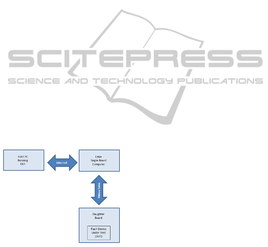
5 THE TOOL CHAIN
The tool chain developed for use in this project is
comprised of a NAND Flash Utility Tester, Environ-
mental Oven and Graphical User Interface (GUI).
Figure 6: Overview of test system.
As shown in Figure 6, the GUI is installed on a
computer, with the tester units connected via Ether-
net cables. These, in turn, are connected to daughter
boards, on which the Devices Under Test (DUT) are
placed. On initialising the GUI a TCP/IP connection
to the Linux on the tester unit is opened. A grammar
of commands are then used in order to run program,
read and erase operations, among other operations.
The Environmental Oven is used to run temperature
controlled test cycles - the oven is ported so the tester
units can go directly into these ovens.
6 CURRENT POSITION
To date, the research project has completed a num-
ber of phases. Firstly, an Non-Disclosure Agreement
(NDA) is in place with a manufacturer. This allowed
for the receipt of a batch of preproduction TLC Flash
part samples and a preliminary datasheet. Following
this, an initial set of tests was performed. These tests
allowed us to specify a new driver requirement for the
existing tester. This will require software and hard-
ware modification to support the new device and this
work is currently ongoing.
7 FUTURE WORK
Plans for future work include completing a block map
layout of the TLC chip and then comparing it to the
one outlined by Yakoobi (Yaakobi et al., 2012). A lay-
out of error mapping across blocks and pages in TLC
chips will be completed, with the results then com-
pared to those found by Cai (Cai et al., 2012), when
using MLC chips, and Yakoobi (Yaakobi et al., 2012),
when using TLC chips from another manufacturer.
Following this, ML techniques discussed above will
be applied to classify and optimise the TLC chips.
8 CONCLUSIONS
This paper has provided an introduction to Flash
memory and an outline of how ML has been shown to
improve NOR, and to classify MLC NAND. Current
research on TLC NAND has also been introduced,
along with a description of this project. We plan to use
ML to characterise and optimise reliability of TLC,
the results of which will provide important data on
TLC memory. This is needed in order to further the
understanding of this technology.
ACKNOWLEDGEMENTS
The author would like to thank the paper’s reviewers
and Barry Fitzgerald.
TheCharacterisationandOptimisationofTLCNANDFlashMemoryusingMachineLearning-APositionPaper
563

REFERENCES
Aritome, S., Shirota, R., Hemink, G., Endoh, T., and Ma-
suoka, F. (1993). Reliability issues of flash memory
cells. Proceedings of the IEEE, 81(5):776 –788.
Bez, R., Camerlenghi, E., Modelli, A., and Visconti, A.
(2003). Introduction to flash memory. Proceedings
of the IEEE, 91(4):489 – 502.
Cai, Y., Haratsch, E., Mutlu, O., and Mai, K. (2012). Er-
ror patterns in mlc nand flash memory: Measurement,
characterization, and analysis. In Design, Automation
Test in Europe Conference Exhibition (DATE), 2012,
pages 521 –526.
Compagnoni, C., Miccoli, C., Mottadelli, R., Beltrami, S.,
Ghidotti, M., Lacaita, A., Spinelli, A., and Visconti,
A. (2010). Investigation of the threshold voltage in-
stability after distributed cycling in nanoscale nand
flash memory arrays. In Reliability Physics Sympo-
sium (IRPS), 2010 IEEE International, pages 604 –
610.
Desnoyers, P. (2010). Empirical evaluation of nand flash
memory performance. SIGOPS Oper. Syst. Rev.,
44(1):50–54.
Grupp, L., Caulfield, A., Coburn, J., Swanson, S., Yaakobi,
E., Siegel, P., and Wolf, J. (2009). Characterizing flash
memory: Anomalies, observations, and applications.
In Microarchitecture, 2009. MICRO-42. 42nd Annual
IEEE/ACM International Symposium on, pages 24 –
33.
Hasler, P. and Lande, T. (2001). Overview of floating-
gate devices, circuits, and systems. Circuits and Sys-
tems II: Analog and Digital Signal Processing, IEEE
Transactions on, 48(1):1 –3.
Hemink, G., Tanaka, T., Endoh, T., Aritome, S., and Shi-
rota, R. (1995). Fast and accurate programming
method for multi-level nand eeproms. In VLSI Tech-
nology, 1995. Digest of Technical Papers. 1995 Sym-
posium on, pages 129 –130.
Hogan, D., Arbuckle, T., and Ryan, C. (2012a). Evolv-
ing a storage block endurance classifier for flash mem-
ory: A trial implementation. Not yet published. Pre-
sented at 11th IEEE International Conference on Cy-
bernetic Intelligent Systems 2012, University of Lim-
erick, Limerick, Ireland.
Hogan, D., Arbuckle, T., Ryan, C., and Sullivan, J. (2012b).
Evolving a retention period classifier for use with flash
memory. ECTA, Not yet published. To be published
- in Proceedings of 4th International Conference on
Evolutionary Computation Theory and Applications
(ECTA 2012).
IEEE (1998). Ieee standard definitions and characterization
of floating gate semiconductor arrays. IEEE Std 1005-
1998. Endurance: Pg 86, Section 7.
JEDEC (2011). Stress-Test-Driven Qualification of Inte-
grated Circuits - JESD47H-01. Jedec Solid State
Technology Association, Published by JEDEC Solid
State Technology Association 2011 3103 North 10th
Street, Suite 240 South Arlington, VA 22201.
KonceptAnalytics (2010). Global flash memory mar-
ket report - 2010 edition. Market Report SKU:
KOAN2835768 48 Pages, MarketResearch.com. Ac-
cessed on: 11/10/2012.
Koza, J. R. (1992). Genetic Programming: On the Pro-
gramming of Computers by Means of Natural Selec-
tion. Number ISBN 0-262-11170-5. The MIT Press,
Available from: The MIT Press.
Lee, S. S. (2011). Emerging challenges in nand flash
technology. Keynote 6, page 4. Flash Product Plan-
ning Group, Hynix Semiconductor Inc., Flash Mem-
ory Summit.
Micheloni, R., Marelli, A., and Ravasio, R. (1998). Error
Correction Codes for Non-Volatile Memories, volume
XII. Springer.
Pavan, P., Bez, R., Olivo, P., and Zanoni, E. (1997). Flash
memory cells-an overview. Proceedings of the IEEE,
85(8):1248 –1271.
Suh, K.-D., Suh, B.-H., Um, Y.-H., Kim, J.-K., Choi, Y.-
J., Koh, Y.-N., Lee, S.-S., Kwon, S.-C., Choi, B.-S.,
Yum, J.-S., Choi, J.-H., Kim, J.-R., and Lim, H.-K.
(1995). A 3.3 v 32 mb nand flash memory with in-
cremental step pulse programming scheme. In Solid-
State Circuits Conference, 1995. Digest of Technical
Papers. 41st ISSCC, 1995 IEEE International, pages
128 –129, 350.
Sullivan, J. and Ryan, C. (2007). A destructive evolutionary
algorithm process. In Frontiers in the Convergence of
Bioscience and Information Technologies, 2007. FBIT
2007, pages 761 –764.
Tanaka, T., Tanzawa, T., and Takeuchi, K. (1997). A 3.4-
mbyte/sec programming 3-level nand flash memory
saving 40size per bit. Technical Report 4-93081 3-76-
X, Symposium on VLSl Circuits Digest of Technical
Papers. Pages 65 - 66.
Tewksbury, S. K. and Brewer, J. E. (2008). Nonvolatile
Memory Technologies with Emphasis on Flash. IEEE
Press Series on Microelectronic Systems. IEEE Press
Series, 445 Hoes Lane, Piscataway, NJ 08854.
Yaakobi, E., Grupp, L., Siegel, P., Swanson, S., and Wolf,
J. (2012). Characterization and error-correcting codes
for tlc flash memories.
Yaakobi, E., Ma, J., Grupp, L., Siegel, P., Swanson, S.,
and Wolf, J. (2010). Error characterization and coding
schemes for flash memories. In GLOBECOM Work-
shops (GC Wkshps), 2010 IEEE, pages 1856 –1860.
ICAART2013-InternationalConferenceonAgentsandArtificialIntelligence
564
