
Use of Partial Reconfiguration for the Implementation and
Embedding of the Artificial Neural Network (ANN) in FPGA
Carlos Alberto de Albuquerque Silva, Anthony Andrey Ramalho Diniz,
Adrião Duarte Dória Neto and José Alberto Nicolau de Oliveira
Universidade Federal do Rio Grande do Norte – UFRN, Natal- RN, Brazil
Keywords: FPGA, Partial Reconfiguration, Artificial Neural Networks.
Abstract: This paper is focused on partial reconfiguration of Field Programmable Gate Arrays (FPGAs) Virtex
®
-6,
produced by Xilinx
®
, and its application implementing Artificial Neural Networks (ANNs) of Multilayer
Perceptron (MLP) type. This FPGA can be partially reprogramed without suspending operation in other
parts that do not need reconfiguration. It can be performed by specifying the Modular Project’s flow, where
the modules that compose the project can be synthesized separately, and, after that, reunited in another
module of highest hierarchical level. Alternatively, it is possible developing reconfigurable modules
inserted in partial bitstreams and, later, downloading partial bitstreams successively in hardware. Therefore,
it is possible configuring topologies of different MLP networks by using partial bitstreams in reconfigurable
areas. It is expected that, in this kind of hardware, applications with MLP ANNs be easily embedded, and
also allow easily configuration of many kinds of MLP networks in field.
1 INTRODUCTION
In the modern industry, designing, building and
managing “information”, as a strategy of supporting
system monitoring and controlling processes, are
extremely important to the whole industry,
especially to processes under uncertainties and with
incomplete data. Dealing with this strategy has
demanded improvements in computational systems,
making them answer faster or even in real time. It is
also observed that, when processing information,
some applications require many resources when
dealing with sequential architectures.
In this context, performance requirements of
many applications are not met, when running
through conventional computational systems, which
have only one sequential processor, based on Von
Neumann Architecture. This architecture does not
incorporates any kind of intelligence in machine
actions, but only runs commands given by some way
of algorithm. To circumvent this problem, artificial
neural networks arise as a solution, allowing, thus,
interpreting and connecting data and instructions
through intelligent decisions. Systems based on
ANNs are substantiate in the belief that intelligent
behavior can be performed only with a huge parallel
processing and data distribution, as happen in
neuronal connections of human beings (Haykin,
2001).
As a result of those limitations imposed by the
Von Neumann model, many implementations of
ANNs began to be developed in hardware, trying to
explore the intrinsical parallelism of those networks.
In many practical applications, particularly the
embedded ones, it is verified that using Field
Programmable Gate Arrays (FPGAs) has allowed
overcoming the missing flexibility of
implementations based on Application Specific
Integrated Circuits (ASICs) (Braga, 2005).
By employing FPGAs as a platform for
implementing ANNs in integrated circuits, it has
been allowed exploring their high power of
processing, portability, consumption without losing
performance, low availability of memory, and ability
of reconfiguring its circuit, what makes the network
adaptable to different applications. Even though,
there are some barriers to a more generic adoption of
this kind of implementation, related to the
development of the artificial neuron, together with
its internal structures: multiplier, activation function
and other parts that, eventually, can be needed
(Silva, Neto, Oliveira and Melo, 2009).
To overcome those barriers and reach more
142
Alberto de Albuquerque Silva C., Andrey Ramalho Diniz A., Duarte Dória Neto A. and Alberto Nicolau de Oliveira J..
Use of Partial Reconfiguration for the Implementation and Embedding of the Artificial Neural Network (ANN) in FPGA.
DOI: 10.5220/0004716301420150
In Proceedings of the 4th International Conference on Pervasive and Embedded Computing and Communication Systems (PECCS-2014), pages
142-150
ISBN: 978-989-758-000-0
Copyright
c
2014 SCITEPRESS (Science and Technology Publications, Lda.)

flexibility in topological configuration of neural
networks, it is needed using FPGAs, which allow the
dynamic and partial reconfiguration of neuronal
connections. Those characteristics can be found in
Virtex
®
family FPGAs, produced by Xilinx
®
.
These FPGAs can be integrated in a
computational system and configured during
runtime, which allows implementing a specific
software function with high performance. They can
also be partially reprogramed without suspending
operation of some parts that do not need to be
reconfigured. This last function can be performed by
specifying the flow of modular project, where the
modules that compose the project can be synthesized
separately and, after that, reunited in a module of
highest hierarchical level. Alternatively, it is
possible developing reconfigurable modules inserted
in partial bitstreams and, after that, making
successive downloads of those partial bitstreams in
hardware (Xilinx, 2010).
In this context, this paper aims at studying the
flow of modular project to implement and partially
reconfigure FPGA Virtex
®
-6, describing MLP
ANNs. The modular project will contain
reconfigurable modules of MLP networks, which
will be transferred to the hardware in distinct
moments.
This paper has the following structure: section 2
presents theoretical basis to comprehend artificial
neural networks (ANNs); partially reconfigurable
devices, in this case, Virtex
®
-6 FPGA, produced by
Xilinx
®
, and some aspects that have to be considered
when implementing ANNs in FPGA; section 3
describes the methodology applied to develop the
project and solutions used to implement it; section 4
presents some results obtained after implementing
an ANN in FPGA; and, finally, section 5 presents
conclusions.
2 THEORETICAL BASIS
Next, is presented a brief review about the
theoretical bases that support this project, whose
objective is giving the ground needed to this
research.
2.1 Artificial Neural Networks (ANNs)
Computational systems based on conexionist
methods of artificial neural networks (ANNs) show
effectiveness, behaving different from conventional
computational programs, which calculate solutions
to a problem, anticipating all the conditions to the
input data to forecast outputs. Conexionist
computational systems try to simulate the behavior
of the human brain, acquiring knowledge to the
solution of a given problem through the processes of
learning and generalization (Haykin, 2001).
ANNs are widely applied in tasks like: function
approximation, time series and forecasting,
classification and standards recognition. Even
having these advantages and applications, those
kinds of systems have some deficiencies, like taking
too long during the training phase, having a high
computational cost, and behaving like a black box
after the training (Prado, 2011).
2.1.1 The Representation of Artificial
Neurons
The model of artificial neurons adopted in this paper
was the perceptron, proposed by McCulloch and
Pitts (1943). This model was chosen because it
establishes the basis for many existing networks, and
their ability for learning, which occurs through the
solution of an optimization problem. This model has
a limitation of processing only problems with
linearly separable data sets (Figure 1), i. e., data sets
that have a well-defined boundary region between
the classes, which can be limited by a line (Haykin,
2001).
Figure 1: Linearly separable classes.
Related to the functional perspective, the neuron
functionality can be defined in terms of the
mathematical model of a perceptron (Figure 2),
which is constituted by a transfer function (sum)
followed by an activation function. The scalar
product of inputs and synaptic weights, whose result
is added to the threshold, compose the transfer
function. The result of this function is, then, passed
to the activation function that, for this task, can be of
sigmoidal or hyperbolic tangent types.
2.1.2 Multilayer Perceptron (MLP)
When working with ANNs to solve some given
UseofPartialReconfigurationfortheImplementationandEmbeddingoftheArtificialNeuralNetwork(ANN)inFPGA
143
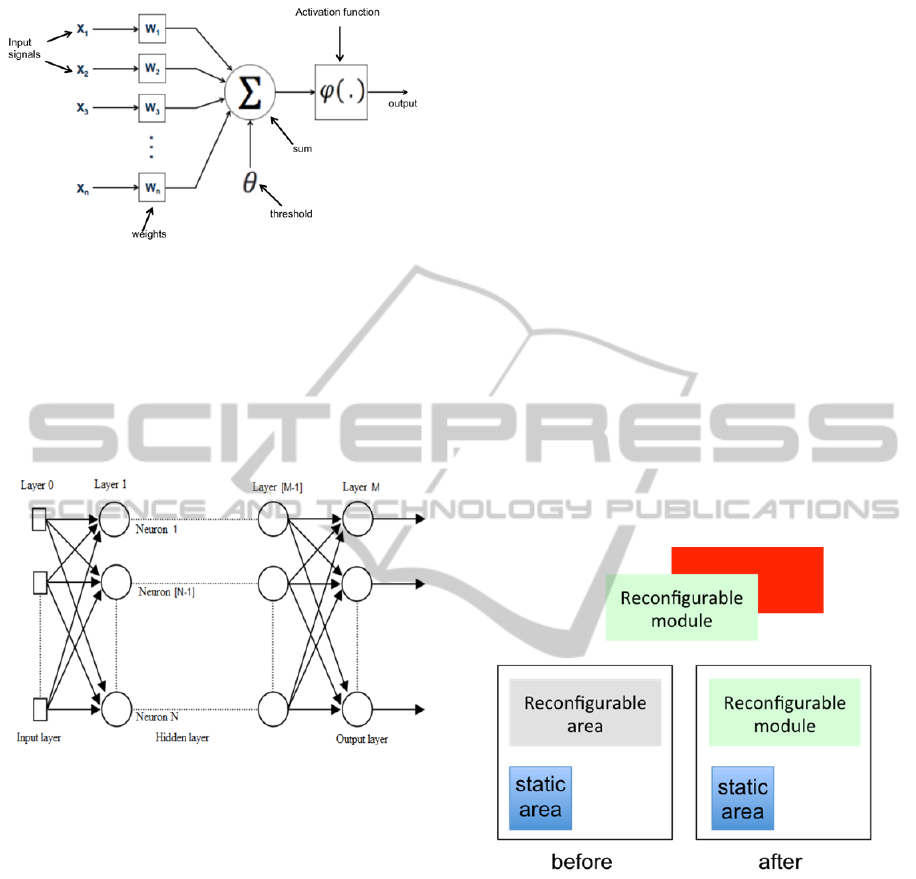
Figure 2: Schematic model of a perceptron.
problem, it has to be defined some architecture, the
learning method and an algorithm for learning. In
this paper, it was applied the Multilayer Perceptron
(MLP) architecture, which is characterized by being
a network fed forward with artificial neurons
(perceptrons) disposed in one input layer, one or
more hidden layers, and one output layer (Figure 3).
Figure 3: Multilayer Perceptron (MLP).
In this kind of architecture, the supervised
learning method is characterized by the presentation
of pairs of examples for inputs and desired outputs,
which are compared with the real network outputs,
with the aim of adjusting its parameters, such as
synaptic weights and threshold, and also minimize
the difference between the real and desired outputs.
To reach this goal, the backpropagation algorithm
can be used as learning algorithm and to correct
errors (Haykin, 2001).
2.2 Partial Reconfiguration of
Hardware
During the last decade, it has been observed that
many projects of embedded systems have been
adopting more and more reconfigurable chips (Field
Programmable Gate Arrays – FPGA) for different
types of applications. The hardware that uses this
kind of chip is different from the static one
(Application-Specific Integrated Circuit – ASIC),
because of its flexibility of changing its internal
architecture during the execution time, which is a
process made by software without turning the
hardware off (Vahid, 2007).
The application of partial reconfiguration has
been motivated by two distinct conditions: the first
one is the existence of idle or underutilized
hardware, and the second one is the need of
partitioning a big system to limited FPGA resources.
Because of that, advances in the newest FPGA
technology have given support to two kinds of
reconfiguration: the static and the partial. The static
reconfiguration refers to the ability of performing a
total reconfiguration of the chip, but once
programmed, its configuration remains in the FPGA
while the application is running. On the other side,
the partial reconfiguration (Figure 4) is defined as
the selective update of one or more subsections of
FPGA and its routing resources, while the rest of the
programmable resources of that device keep running
during the reconfiguration time (Mesquita, 2003).
Figure 4: Partial reconfiguration.
The partial reconfiguration has provided
expressive benefits to systems that demand
flexibility, high performance, high data-transfer rate
and efficiency of energy consumption, as it
minimizes hardware resources demanded. Many
applications have been reported in areas that include
image processing (Manet, 2008), artificial neural
networks (Upegui, Peña-Reyes, Sánchez, 2003)
,
computational vision (Sen, 2005
)
and genetic
algorithms.
Besides the benefits listed before, the partial
reconfiguration presents also some disadvantages,
being the complexity of working with dynamic
allocation the most complex one. Changes
PECCS2014-InternationalConferenceonPervasiveandEmbeddedComputingandCommunicationSystems
144

performed by the dynamic allocation, during the
running time, make harder understanding the exact
system behavior, being needed a previous
understanding of all the possible running sequences.
2.2.1 The Architecture of Reconfigurable
FPGAs
Xilinx is among the pioneer companies in
developing FPGAs that allow partial
reconfiguration.
FPGAs from the Virtex family have
configurable logic blocks (CLBs), input/output
blocks (IOBs), random access memory blocks
(RAMs), clock resources, programmable routing and
electrical circuit configuration. Each CLB has
resources for local routing and a connection to the
general routing matrix (GRM). A peripheral routing
ring, named VersaRing, allows additional routing
with input and output blocks (IOBs).
RAM blocks, presented by this architecture, are
dual-port type, with reading and writing channels,
where is possible running simultaneously these two
options with distinct addresses. Those FPGAs have
also blocks that implement DLLs functions to
control, distribute and compensate clock delay
(Xilinx, 2010).
Figure 5 shows an abstraction of the internal
FPGA Virtex architecture.
Figure 5: FPGA Virtex architecture.
Device functionalities are defined through the
configuration file, named bitstream, which have a
mix of commands and data. They can be red and
written through some of the Virtex configuration
interfaces. Virtex devices have the internal
architecture organized in columns (Figure 5) that can
be individually red and written. Thus, it is possible
partially reconfigure those devices through the
change of those columns in the configuration file
(Mesquita, 2003).
2.3 ANNs Implemented in FPGA
Literature presents some examples of artificial
neural networks implemented in FPGA. Some of
those networks adopt the Very High Speed
Integrated Circuit Hardware Description Language
(VHDL) as input method, which is a language
supported by most of the synthesis tools. VHDL
allows that complex circuits to be designed from a
structural model, data flow and behavioral
description.
To implement an ANN through reprogrammable
devices, both input and output values must be
processed in fixed point arithmetic, as a way of
adapting it to the digital architecture of FPGAs.
Thus, it has to be determined the amount of bits to
the number representativeness, taking into account
the accumulation of errors to be generated through
the fixed point calculation, when despising truncated
data (Himavathi, Anitha and Muthuramalingam,
2007) and (Silva, Dória Neto, Oliveira and Melo,
2010). Alternatively, it can be chosen working with
a hybrid combination of fixed and floating
arithmetic. In this context, some bits are split to
define mantissa, exponent, sign and a fixed offset,
which allows representing the value in floating point
(Wiist, Kasper, Reininger, 1998).
The neural architecture proposed by (Silva,
2010) implements an artificial neuron, as the basic
processing unit, and replicates it, in the sequence, to
create an MLP network.
Embedded systems, in just one only chip, have a
large industrial acceptance. With this goal, (Lopes
and Melo, 2009) developed a set of specialists in just
one committee machine, using the Nios
®
II
processor, synthesized in FPGA. Such proposal
intended to solve problems with highest complexity,
which need more than one evaluator expert system.
3 THE PROJECT
In this research, it was used the ISE 14.2 and
PlanAhead 14.2 tools, by Xilinx, and partial
reconfiguration based on modules, because the
methodology adopted by Xilinx tools has changed
drastically in the last years, especially after the
macros bus, which allows manual routing, needed to
communicate modules. PlanAhead allows creating
reconfigurable partitions in FPGA and also setting
each of those reconfigurable regions. Besides that, to
make this reconfiguration possible, it is needed that
the FPGA supports this functionality, and also a
UseofPartialReconfigurationfortheImplementationandEmbeddingoftheArtificialNeuralNetwork(ANN)inFPGA
145
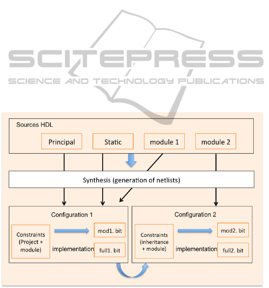
specific communication port to that, as the Internal
Configuration Access Port (ICAP) (Xilinx, 2010).
Each configuration meets the FPGA’s static parts
– clock managers, processors, buses – with the
specific dynamic part. When a configuration
changes only one region, it imports data about pins
from other partitions, with which occurs
communication. From each configuration is possible
generating a bit file that can be charged to partially
or totally reconfigure the FPGA.
The project flow to partially reconfigure (Figure
6) consists, initially, of describing functions that the
hardware will have to run, through the hardware
description language (HDL). Thus, it is possible
synthesizing the modules to make possible
connecting them, and using PlanAhead. Before
generating each partial or full bit file, it is needed
adding board and project constraints, being the file
responsible for defining the minimum delays in
communication between modules; pins, where input
and output data are connected; and the slice
coordinates that bound each reconfigurable region.
Next subsection will present methods applied in
this project to implement ANNs with partial
dynamic reconfiguration.
3.1 The Perceptron in FPGA
Having as reference the neuron proposed by
McCulloch and Pitts (Figure 2), the architectures
proposed for neurons in this paper followed the
model developed by (Silva, 2010), using VHDL,
showed in Figure 7. Those two architectures were
divided in two functional blocks: the first one is a
linear combiner, responsible for adding the inputs
pondered by synaptic gains; and the second one is
responsible for calculating the activation function,
named, respectively, NET and FNET blocks.
The construction of those blocks is based on the
RTL design approach (project in transfer level
among records), including registers to synchronize
the data flow.
3.1.1 Static Neuron
The static and total implementation of FPGA, the
NET block (Figure 7), besides calculating the
induced perceptron local field with up to eight inputs
of 16 bits, which are imposed to it, also presents the
data flow among MULT and ADDER blocks.
To keep parallelism, each neuron input is
directed to an exclusive multiplier that performs
Figure 6: Design flow for partial reconfiguration.
PECCS2014-InternationalConferenceonPervasiveandEmbeddedComputingandCommunicationSystems
146
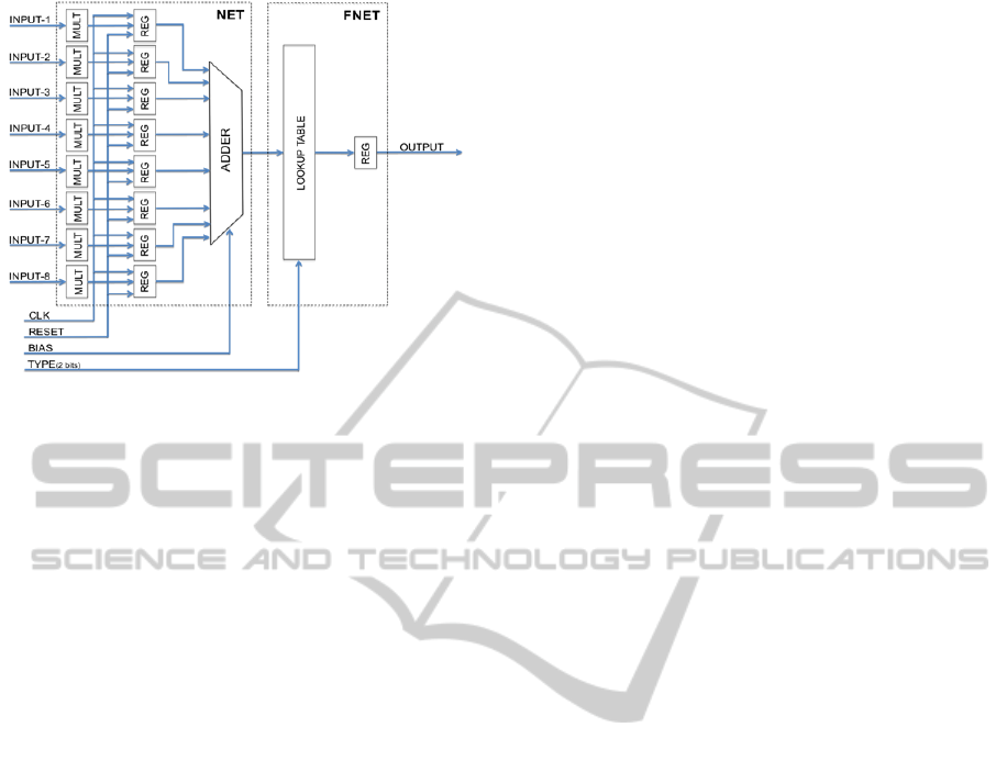
Figure 7: Proposed structure of the neuron in hardware.
the product with the synaptic weight, both defined in
fixed point with sixteen bits and sign. In each
MULT block is performed the shifting of sixteen
bits to keep the compatibility with the fixed point
representation of system data. The ADDER block is
the unit responsible for adding the results from
multiplication and threshold.
To conclude the NEURON block, after the
calculation of the induced local field, it is performed
the calculation of the activation function, in the
FNET block. In this calculation, it can be chosen
using sigmoid or tangent sigmoid activation
functions, calculated as described in section 3.2.
3.1.2 Dynamic Neuron
The description of NEURON block, with partial
reconfiguration, is different from the static
description only because of the FNET block. This
block has two reconfigurable modules, one for each
activation function, which are translated in BIT
partial files. Those files are selected and downloaded
to some reconfigurable regions of FPGA, by a
controller (state machine) that will define a new
functionality to the artificial neuron.
3.2 The Calculation of the Activation
Function
The implementation of the sigmoid or hyperbolic
tangent activation function in FPGA is performed by
applying a lookup table (LUT), whose structure is
constituted by a comparator block, and two 16 x 21
data bits parallel ROMs. The reason why a lookup
table is chosen to simulate the tangent sigmoid
function is related to the cost and the difficulty of
implementing it mathematically in FPGA. The
applied activation function is constituted by a table
of 21 points with previously defined values (Silva,
2006).
To define this function, the solution adopted was
representing the function by the set of linearly
interpolated points, in such a way that the difference
between the curves of the function and of the points
be minimal. To reach this goal, it was applied the
computational intelligence technique, known as
genetic algorithm, which is intended to achieve the
smallest error for each individual, based on some
objective function.
After running the genetic algorithm, it was
obtained 21 points showed in table x, corresponding
to the x road function of the sigmoid tangent and
their respective y outputs. Thus, it was obtained the
angular and linear coefficients, stored in the ROM of
the LUT unit.
So, the calculation of the output value of the
FNET block is executed in the following way: from
the input value (from the NET block), it is defined a
LUT address common to both ROMs, where are
stored the angular and linear coefficients of the line
segment, to be used by the interpolator block, to
generate the output signal.
3.3 Structural Descriptions of Neural
Networks in FPGA
Solutions proposed to enable studying ANNs with
partial reconfiguration of FPGA were based on
describing the NEURON block using VHDL. By
this way, the natural flow of implementation was
describing the neural network architecture, through
the replication of NEURON block.
By using this solution, there were built three
structures to replicate the NEURON block, being
them all MLPs. The first structure was a network
with two inputs, two neurons in the hidden layer,
and one neuron in the output layer. The second one
was a network with just one input, three neurons in
the hidden layer, and one neuron in the output layer.
The third structure was composed by one input, five
neurons in the hidden layer, and one neuron in the
output layer.
The partial reprogramming of FPGA demands a
control circuit similar to the ones used to reprogram
reconfigurable FPGAs, but having the possibility of
partially reconfiguring it, not totally. The control
circuit must have spare and dynamic releasing
capacities. Every time that some ANN has to be run,
but it is not in the memory yet, it has to be
transferred from the external memory to the
configuration memory of the FPGA. As this kind of
UseofPartialReconfigurationfortheImplementationandEmbeddingoftheArtificialNeuralNetwork(ANN)inFPGA
147
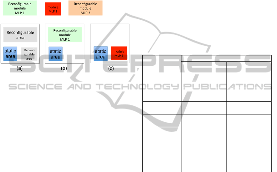
FPGA has a symmetric architecture, it is noted that
the same ANN will probably work in the same way,
independent from the zone it is charged in FPGA.
On the other side, every time that is needed to run a
new ANN, which is not changed in FPGA, without
having some available zone, it has to select among
mapped blocks some of them that are not being
needed or temporary suspended, transferring the new
block to it (Figure 8).
Figure 8: Partial reconfiguration ANN.
4 RESULTS AND DISCUSSION
All the results were obtained through simulations
and tests using ISE
®
13.2 and planhead
®
softwares,
both produced by Xilinx
®
, and also through circuit
synthesis information in a FPGA with reference
number XC6VLX240T, Virtex
®
-6.
Architecture was tested using three problems
related to neural networks, such as the XOR
problem, interpolation of Sinc and exponential
functions.
Neural network topologies used for solving
previously mentioned problems were defined and
tested in software. To select the topologies used in
those problems, a simplified heuristic was used. The
heuristic used to define the topology was to create a
small network, with a few NEURON blocks, and the
amount of NEURON blocks was increased until the
network output error was minimal. Between each
increasing of the amount of NEURON block, during
the training, the learning parameter was modified to
adapt it to each network topology. These weights
and thresholds were then normalized and
transformed into a fixed point. After data were
obtained simulations and syntheses of the system in
the hardware implemented can begin. Only after
obtaining those data from software, it could be
possible implementing them on hardware.
4.1 Synthesis Results
In this section, it is possible verifying a comparative
between occupation rates of two MLP network
architectures through FPGA.
The architecture proposed by (Silva, 2010) was
composed by seven NEURON blocks, being one of
them for the input and the other one for the output
layers. Thus, the architecture proposed in this study
was composed by three neurons in the hidden layer
and one for the input and the other one for the output
layer. The proposed architecture resulted in
increasing 2% in the amount of logical units when
compared to the previous implementation. This
increasing occurs because of the partial bitstreams.
Table 1: FPGA Area Analyses.
Architectures
Comparison
Architectures Comparison
Architecture
proposed in this
study
Architecture
proposed in
(Silva, 2010)
Device
XC6VLX240T
EP2C35F672C6
Logical
elements
6,375/37,680
(14%)
3,975/33,216
(12%)
Number of
registers
768 482
Number of
pins
536/832 (78%) 458/475 (96%)
Number of
bits of
memory
1/14,976 (0%) 0/483.840 (0%)
Dedicated 9-
bit multiplier
32/90 (40%) 32/70 (46%)
Clock
frequency
62.32 MHZ 55.92 MHZ
Table 1 presents a comparison between
characteristics of FPGA synthesis in the architecture
proposed here and the others discussed in this study.
Maximum working frequency that the device can
operate at is 62.32 MHz, a good index when
compared with architectures developed by other
authors exhibited in Table 1. Information about
maximum working frequency was obtained using
Xilinx ISE Design Suite 13.2 software.
Another point to observe is the energy analysis of
the device, considering costs involved in
implementing an MLP-type ANN. Total thermal
energy dissipated by the device is 242.34 mW. This
energy is partially dissipated by the input and output
drives (87.23mW), while the other part occurs
through dissipation of static thermal energy in the
core. The maximum current drained by the
architecture will be 155.03 mA, internally, and 17.06
mA at the input and output pins. These data were
PECCS2014-InternationalConferenceonPervasiveandEmbeddedComputingandCommunicationSystems
148
based on analysis performed by Xilinx ISE
software.
4.2 Results from Simulations
In this section, it is shown results from processing
MLP networks to solve the classification problem of
XOR logical function and interpolation problems of
Sinc and Exponential functions. Those networks
were previously trained and tested by software.
To run the XOR function, it was used an MLP
network with two inputs, two neurons in the hidden
layer, and one neuron in the output layer. To the
activation functions, it was used partial bitstreams,
which configured the MLP network outputs. It was
observed that, implementing this neural network,
following the given model, taken to solving the
XOR problem, and the output values are shown in
Table 2. They show that the implementation using
Vitex-6 FPGA is valid, once the maximum relative
error was just 0.25%.
Table 2: Comparative results of the neural network used
for implementation of the XOR.
Input
Output
(software)
Fixed
point
Output
(FPGA)
Function
Sigmoid
Output
(FPGA)
Function
Sigmoid
tangent
00
103 105 105
01
5657 5651 5651
10
5679 5672 5672
11
91 90 90
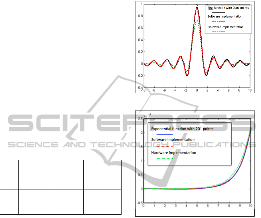
Figure 9 shows a comparative between software
and hardware implementation of Sinc function. The
implemented MLP network was composed by one
input, five neurons in the hidden layer, and one
neuron in the output layer, both with hyperbolic
tangent activation function.
Figure 10 shows another comparative, but it is
between software and hardware implementation of
Exponential function. The implemented MLP
network was composed by one input, three neurons
in the hidden layer, and one neuron in the output
layer, both with sigmoid tangent activation function.
5 CONCLUSIONS
FPGA, in running time, makes the reconfiguration
flexibility wider and reduces the silicon area,
allowing reprograming it in field. As a result of the
new FPGA tools, projects of partial reconfiguration
Figure 9: Comparative Sinc function.
Figure 10: Comparative Exponential function.
were made simple, reducing their complexity and
the project’s time market.
In this context, it was performed a description of
one neuron, using numerical notation of fixed point
and by employing a partial reconfiguration strategy
to implement sigmoid and hyperbolic tangent
functions. To those functions, data was obtained
from linear interpolation, using lookup table.
By specifying the NEURON block, constituted
by NET and FNET blocks, it was verified that, in
this study, the used architecture descriptions become
very modular, making possible easily increase and
reduce the number of neurons, and also the network
structure. As a result, there were created partial
modules of complete neural networks in Virtex-6
FPGA, with the proper numerical precision and high
ability of parallel processing.
The MLP architectures, developed in partially
reconfigurable Virtex-6 FPGA, allowed qualifying
UseofPartialReconfigurationfortheImplementationandEmbeddingoftheArtificialNeuralNetwork(ANN)inFPGA
149

the methods and approaches developed in this study
as able to being transported from the simulation
phase to real systems, complying with the
established requirements for the project.
In future, it is planned to create a Graphical User
Interface (GUI) as an easy way of specifying other
ANNs.
ACKNOWLEDGEMENTS
Authors would like to thank to PRH-ANP 14, for
financial support; and professors of PPGEEC
(Programa de Pós-Graduação em Engenharia
Elétrica e da Computação) and PPGCEP (Programa
de Pós-Graduação em Ciência e Engenharia de
Petróleo).
REFERENCES
Braga, A. L. S., Llanos, C. H., Ayala-Rincón, M., Jacobi,
R.P., 2005. VANNGen: a Flexible CAD Tool for
Hardware Implementation of Artificial Neural
Networks. International Conference or Reconfigurable
Computing and FPGAs - Reconfig05. Sep. 28-30.
Haykin, S., 2001. Neural Networks: A Comprehensive
Foundation. 2. ed. Porto Alegre: Bookman, 900 p. 20.
Himavathi, S., Anitha, D. Muthuramalingam, A., 2007.
Feedforward Neural Network Implementation in
FPGA Using Layer Multiplexing for Effective
Resource Utilization. IEEE Transactions On Neural
Networks, Vol. 18, No. 3.
Lopes, D. C., Melo, J. D., Neto A. D. D., 2009.
“Implementation and Evaluation of a Modular Neural
Network in a Multiple Processor System on Chip”. In:
The 12th IEEE International Conference on
Computacional Science and Engineering CSE, 2009,
Vancouver. IEEE International Conference on
Computacional Science and Engineering, v. 1. p. 412-
417.
Manet, P., 2008. An evaluation of dynamic partial
reconfiguration for signal and image processing in
professional electronics applications. EURASIP
Journal on Embedded Systems. Article No. 1.
Mesquita, D. G., 2003. Remote and Partial
Reconfiguration of FPGAs: tools and trends.
Proceedings of the International Parallel and
Distributed Processing Symposium (IPDPS’03).
Prado, R. N A., Silva, C. A. A., Oliveira, J. A. N., Doria
Neto, A. D., Melo, J. D, 2011. FPGA Based
Architecture For Easy Configuration Of Multilayer
Perceptron Neural Network Topologies. X Brazilian
Congress in Computational Inteligence – X CBIC.
Sen, M., 2005 .Computer Vision on FPGAs: Design
Methodology and its Application to Gesture
Recognition. Computer Vision and Pattern
Recognition - Workshops, 2005. CVPR Workshops.
IEEE Computer Society Conference on.
Silva, C. A. A., 2010. Contribuição para o estudo do
embarque de uma rede Neural artificial em field
programmable gate array (FPGA).
Silva, C. A. A., Neto, A. D. D, Oliveira, J. A. N., Melo, J.
D., 2009. Implementation of an Artificial Neural
Network on FPGA : Application of MLP as Modular
Architecture. IX Brazilian Congress of Neural
Networks Computational Intelligence - IX CBRN,
Ouro Preto, October.
Silva, D. R. C., Neto, A. D. D., Guedes, L. A., Melo,
2006. Neural Networks Implementation in Foundation
Fieldbus Environment: A Case Study in Neural
Control. International Journal of Factory Automation,
Robotics and Soft Computing, v. 3, p. 48-54.
Vahid, F., 2007. Digital Design. Wiley.
Upegui, A., Peña-Reyes, C. A., Sánchez, E., 2003. A
methodology for evolving spiking neural-network
topologies on line using partial dynamic
reconfiguration.
Xilinx, 2010. Partial Reconfiguration User Guide.
Wiist, H., Kasper, K., Reininger, H., 1998. Hybrid
Number Representation for the FPGA-Realization of a
Versatile Neuro-Processor. Euromicro Conference,
1998. Proceedings 24th. Vol. 2, D.O.I
10.1109/EURMIC.
PECCS2014-InternationalConferenceonPervasiveandEmbeddedComputingandCommunicationSystems
150
