Concepts and Design of Novel Integrated Photonic Devices based on
Silicon-organic Hybrid Technology
Patrick Steglich
1,2
, Mauro Casalboni
2
and Sigurd Schrader
1
1
Faculty of Engineering and Natural Sciences, University of Applied Sciences Wildau, Wildau, Germany
2
Department of Industrial Engineering, University of Rome ”Tor Vergata”, Rome, Italy
1 RESEARCH PROBLEM
This doctoral thesis is about the development of inte-
grated photonic devices through the implementation
of electro-optical organic materials in a CMOS-like
production line. Slot-waveguide structures are the key
element in order to integrate organic materials into sil-
icon photonics. For that reason, slot-waveguides have
been employed in order to develop high-speed modu-
lators for telecommunication interconnects (Weimann
et al., 2014).
The major advantage of slot-waveguides is the fact
that the guided light is confined in between two sili-
con rails (Almeida et al., 2004). For that reason the
light is forced to interact directly with the surrounding
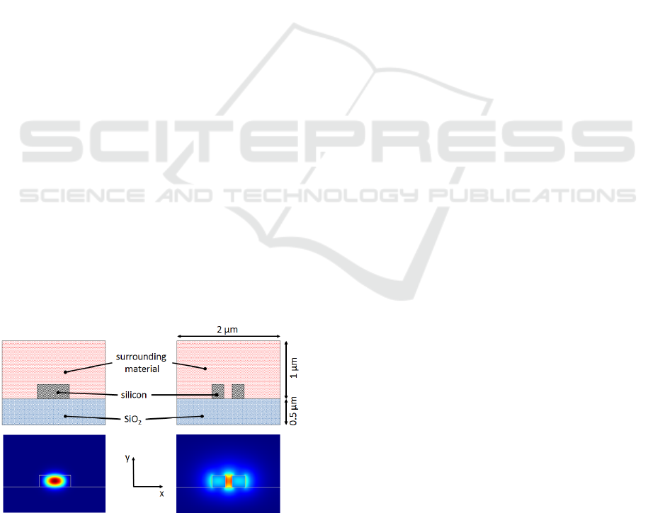
material. Figure 1 shows a detailed cross-sectional
Figure 1: Cross-sectional view of a SOI strip-waveguide
(left) and a SOI slot-waveguide (right). The pictures below
show the optical field amplitude distribution. Both waveg-
uide structures are on top of a buried oxide (BOX) substrate.
The slot-waveguide structure shows enhanced field inten-
sity in the slot interior.
view and compares the guided optical field in a strip-
waveguide to a slot-waveguide.
The reason for this high confinement in-between the
silicon rails is the large-index contrast of the high-
index silicon and the low-index surrounding material.
At the interface the normal electric field, which is ac-
cording to Figure 1 the E
x
field, undergoes a large dis-
continuity. This results in a field enhancement in the
low-index region which is proportional to the ratio of
the dielectric constant of the surrounding material to
that of silicon.
The high confinement inside the slot is of special
benefit for electro-optical applications. The so called
silicon-organic hybrid (SOH) technology uses organic
materials with exceptional high linear electro-optical
coefficients as surrounding material (Leuthold et al.,
2013). Current electro-optic modulators are based on
semiconductors like silicon. In silicon photonics, fun-
damental speed limitations are related to carrier injec-
tion and removal (Vivien and Pavesi, 2013). There-
fore, parametric processes are impaired by nonpara-
metric processes like two-photon absorption and be-
come to the main speed limiting factor. Additionally,
silicon has a lack of linear electro-optical coefficients.
All this can be overcome by using organic materials
with nonlinear optical properties as active material.
The most challenging issue of SOH technol-
ogy based slot-waveguides is the compatibility with
common complementary-metal-oxide-semiconductor
(CMOS) fabrication processes since such integrated
photonic devices need a high integration rate and a
cost efficient mass production environment.
For that reason, one focus of this thesis lies on
design trade-offs and on the development of an ap-
proach in order to improve silicon-on-insulator (SOI)
slot-waveguide structures for a CMOS-like produc-
tion environment.
Beside the theoretical investigations there are sev-
eral critical issues during the fabrication process. The
slot width is limited due to common lithography re-
strictions and has a high side-wall roughness after
etching which leads to optical losses. After the Back-
End-Of-Line (BEOL) which includes the metal con-
tacts, as it can be seen in Figure 2, it is necessary to
open the slot-waveguide structures in order to deposit
the organic material inside the slot interior. This step
is critical because a combination of dry and wet etch-
ing is necessary. Nevertheless, it is necessary in order
to maintain CMOS compatibility before the deposi-
55
Steglich P., Casalboni M. and Schrader S..
Concepts and Design of Novel Integrated Photonic Devices based on Silicon-organic Hybrid Technology.
Copyright
c
2015 SCITEPRESS (Science and Technology Publications, Lda.)
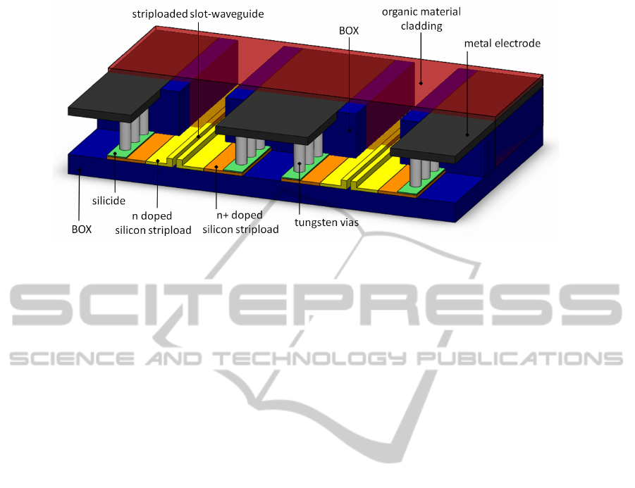
Figure 2: Cross section of two full implemented slot-waveguides with stripload and electrode connection (not to scale). The
slot-waveguide structure has to be opened in order to fill-out the slot with a nonlinear optical cladding. The slot-waveguide
rails are connected by tungsten vias to metal contacts. In this configuration, both slot-waveguides can be used as phase shifter
for a Mach-Zehnder modulator.
tion of organic material.
Selection and deposition of organic materials with
large linear electro-optical coefficients is another crit-
ical task. State of the art SOH modulators using
a novel class of so-called monolithic electro-optic
materials in order to yield high in-device electro-
optic coefficients by avoiding dipole-dipole interac-
tions (Dalton et al., 2010; Palmer et al., 2014).
2 OUTLINE OF OBJECTIVES
The main objective of the thesis is the implementa-
tion of electro-optical organic materials in a CMOS-
like production environment in order to develop inte-
grated photonic devices such as novel electro-optical
modulators based on slot-waveguide structures. Con-
sequently, the scope of this thesis is the conception,
design, and modelling of passive and active photonic
components like strip-to-slot mode-converter, grating
coupler, slot-waveguide structures and electrical con-
tacts. Novel design concepts such as partially slotted
ring resonators and Fabry-Perot-Interferometer with
slotted cavity will be developed. Besides theoretical
investigations, device fabrication and evaluation as
well as deposition of electro-optical organic materi-
als are objectives of the thesis. The organic materials
need to have high thermal, photochemical and long-
term orientational stability as well as a minimized
self-aggregation to avoid scattering losses. Further-
more, large electro-optical coefficients are necessary
in order to reduce the drive voltage of the modulators.
For this reason one part of the thesis is to find ap-
propriate organic materials and deposition methods.
This implies the characterisation of linear and nonlin-
ear optical properties. In order to deposit the organic
materials on the slot-waveguide structure a new ap-
proach will be developed which includes an etching
procedure to open the slot-waveguide structure from
the backside of the SOI wafer.
3 STATE OF THE ART
The Karlsruhe Institute of Technology reported in
2013 and 2014 several silicon-organic hybrid modula-
tors based on a Mach-Zehnder interferometer operat-
ing at 10 Gbit/s, 12.5 Gbit/s, 40 Gbit/s, 84 Gbit/s,
and 112 Gbit/s (Palmer et al., 2013b; Korn et al.,
2013; Leuthold et al., 2013; Palmer et al., 2014; Korn
et al., 2014). They have demonstrated advanced mod-
ulation formats such as 16QAM (Quadrature Am-
plitude Modulation) as well as OOK (On-Off Key-
ing), BPSK (Binary Phase Shift Keying) and 8-ASK
(Amplitude Shift Keying) signals (Korn et al., 2013;
Palmer et al., 2013c). This is possible due to the fact
that organic materials have less free-carrier dispersion
which normally leads to an intrinsic coupling of am-
plitude and phase.
A silicon-polymer hybrid slot waveguide ring-
resonator modulator with a 6 dB bandwidth of 1 GHz,
a device tunability of 12.7 pm/V, and a Q-factor of
5000 were fabricated with 193 nm optical lithography
(Gould et al., 2011).
Palmer et al. published in 2013 strip-to-slot mode-
converter with record-low losses of about 0.02 dB and
negligible reflections between 1480 nm and 1580 nm
(Palmer et al., 2013a). Yang Liu et al. developed in
2011 a so called strip to strip-loaded slot mode con-
verter with losses around 0.81 dB (Liu et al., 2011).
PHOTOPTICS2015-DoctoralConsortium
56
The deposition of organic materials is typically
done by spin-coating but vapour deposition is more
suitable. Spin-coating is critical because the organic
material has to fill-out the interior of the slot homo-
geneously. With spin-coating, it is not guaranteed
that the slot will be filled due to the centrifugal force
and due to the fact that the polymer system is liquid.
With its viscosity and surface tension it precludes the
polymer system from filling out the whole interior of
the slot homogeneously. Commercially available and
reliable organic materials such as M3 (commercial-
ized by GigOptix Inc.) have been successfully used
for several slot-waveguide based electro-optical mod-
ulators like in (Palmer et al., 2013b; Leuthold et al.,
2013; Korn et al., 2013; Palmer et al., 2013c). Special
methods have been developed in order to fill-out the
interior of sub-micrometer slot-waveguide structures
with such solid crystals (Korn et al., 2014). Further-
more, multi-chromophore dendritic molecules, guest-
host and side-chain polymersystems have been used
as electro-optical cladding (Palmer et al., 2014).
In the last decade integrated photonic sensors
based on slot-waveguide ring-resonators have also
been proposed (Dell’Olio and Passaro, 2007) and de-
veloped (Barrios et al., 2007). In case of label-free
bio-sensors it has been shown that the sensitivity of
slot-waveguides is more than three times higher com-
pared to conventional silicon strip-waveguides (Claes
et al., 2009).
There are several publications about field confinement
factors of slot-waveguide structures. These structures
consist of vertical silicon rails (Robinson et al., 2008)
or multiple nanolayers (Feng et al., 2006). However,
none of them consider SOI slot-waveguides with typ-
ical geometrical dimensions for CMOS-like produc-
tion processes.
4 METHODOLOGY
4.1 Simulation of Slot-waveguides
For the calculation of waveguide eigenmodes we em-
ploying a commercial full-vectorial 2D finite element
method (FEM) based mode solver from COMSOL
Multiphysics
r
. Doing this we sweep several param-
eters like the silicon rail width and slot width whereas
the height is fixed to 220 nm. Assuming a wave-
length of 1550 nm, the refractive index for the silicon
is n
si
= 3.48 and for the BOX substrate n
box
= 1.444
(Palik, 1997; Tsang et al., 2002). The refractive index
of the surrounding material n
sm
is variable because
it can be air, gas, fluid or an optical nonlinear mate-
rial, depending on the application. In the following
we will use n
clad
as cladding refractive index instead
of n
sm
because our simulation will use an organic
cladding material. For our simulations we consider
a total domain of D
tot
= 3 µm
2
which is illustrated in
Figure 1.
In order to yield the mode field distribution and
effective refractive index, the refractive index distri-
bution n(x,y) for the structure shown in Figure 1 need
to be declared to calculate eigenvalues and eigenfunc-
tions of the wave equation
∇ × (∇ × E)− k
2
0
n
2
E = 0, (1)
where k
0
is the wave number in free space. By do-
ing this we get the optical field distribution for the
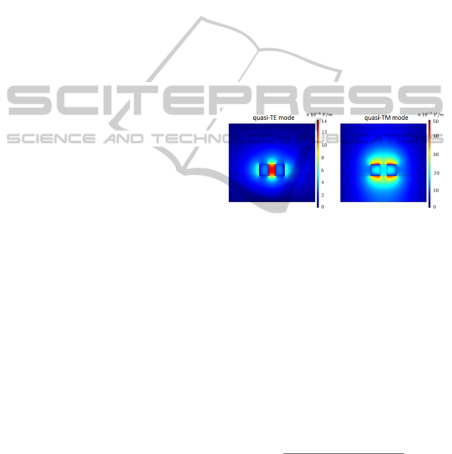
quasi-TE and quasi-TM mode as shown in Figure 3.
In the following we will neglect the quasi-TM mode
because it is over two times of magnitude smaller than
the quasi-TE mode.
Figure 3: Optical field distribution for the quasi-TE and
quasi-TM mode of a SOI slot-waveguide.
4.1.1 Field Confinement Factor of
Slot-waveguides
In order to design, develop and improve slot-
waveguide structures for applications in the field of
biophotonic or high-speed modulators it is necessary
to calculate characteristic values which describe the
confinement and therefore the interaction of light with
the surrounding material. One figure of merit of how
well the guided modal field is confined in a certain re-
gion is the so-called field confinement factor.
The field confinement factor is usually defined as
the ratio of the time averaged power flow in the do-
main of interest (D
int
) to the time averaged power flow
inside the total domain (D
tot
)
Γ =
Z Z
D
int
Re{[E × H
∗
] · e
z
} dxdy
Z Z
D
tot
Re{[E × H
∗
] · e
z
} dxdy
. (2)
E and H are the electric and magnetic field vectors,
respectively, and e
z
is the unit vectors in z direction.
There are three different cases in order to choose
ConceptsandDesignofNovelIntegratedPhotonicDevicesbasedonSilicon-organicHybridTechnology
57

the domain of interest. In case of common strip-
waveguides the domain of interest is equal to the core
region, D
int
=D
core
. In contrast to that, for bio-sensing
applications the region of the cover medium is consid-
ered to be the domain of interest, D
int
=D
cover
, which
is valid for strip- and slot-waveguides as well. Con-
sidering slot-waveguides for electro-optical modula-
tors the domain of interest is equal to the slot region,
D
int
=D
slot
. All possible domains of interest are illus-
trated in Figure 4.
Figure 4: Domains of interest: core D
core
, cladding D
clad
and slot D
slot
regions are highlighted in green.
In case of low-index-contrast waveguides, Equa-
tion 2 can be simplify using the linear relationship
between the electric and magnetic fields
1
2
Z Z
Re{[E × H
∗
] · e
z
} dxdy =
1
2
β
ωµ
0
Z Z
|E|
2
dxdy,
(3)
which leads to
Γ =
Z Z
D
int
|E|
2
dxdy
Z Z
D
tot
|E|
2
dxdy
. (4)
However, for high-index-contrast waveguides and
especially for slot-waveguides this linear relation-
ship does not apply since they must satisfy different
boundary conditions (Robinson et al., 2008). Because
of that, in this work all confinement factors are calcu-
lated according to Equation 2.
4.1.2 Effective Nonlinear Area of
Slot-Waveguides
A figure of merit of how well the waveguide geome-
try supports the nonlinear interaction is the so called
effective nonlinear area (Koos et al., 2007). The
smaller the effective nonlinear area provided by the
waveguide structure the higher the nonlinear interac-
tion which is important for electro-optical modula-
tors.
For the analysis of low-index-contrast systems, it is
usually assumed that the gradient of the dielectric
constant is approximately zero in the entire cross sec-
tion. But this approximation is not valid for high-
index-contrast material systems. Therefore, Koos et
al. derived the effective nonlinear area for high-index-
contrast waveguides in 2007 by using the slowly vary-
ing envelope approximation (Koos et al., 2007). The
effective nonlinear area results then from the nonlin-
ear Schr
¨
odinger equation
A
e f f
=
Z
2
0
n
2
clad
·
Z Z
D
tot
Re{[E × H
∗
] · e
z
} dxdy
2
Z Z
D
int
E
4
dxdy
, (5)
with the free-space wave impedance Z
0
=
p
µ
0
/ε
0
≈
377 Ω. In our case is the domain of interest equal
to the cladding domain, D
int
= D
slot
. In case of low-
index-contrast material systems it can be assumed that
n
core
≈ n
clad
≈ n
box
≈ n
int
, and the longitudinal field
becomes negligible (Koos et al., 2007). Furthermore,
the transverse components of the electrical field E
and the magnetic field H can be approximated by a
scalar function F with the condition E ≈ F · e
x
and
H ≈ (n
int
/Z
0
)F · e
y
where e
x
and e
y
are the unit vec-
tors in x and y direction, respectively (Koos et al.,
2007). Further it can be stated that D
int
= D
tot
if the
nonlinearity is homogeneous in D
tot
. Now Equation
5 becomes simplified to
A
e f f
=
Z Z
D
tot
F
2
dxdy
2
Z Z
D
int
F
4
dxdy
, (6)
which is similar to the common definition of an effec-
tive area (Agrawal, 2012).
4.2 Concept Development and CMOS
Implementation
An appropriate approach to implement nonlinear or-
ganic materials in silicon based fabrication environ-
ment is the use of striploaded slot-waveguides. A
detailed cross sectional view of two parallel im-
plemented slot-waveguides is depicted in Figure 2.
Through a doped silicon stripload and tungsten vias,
the slot-waveguides are directly connected to the
metal electrodes. The tungsten vias are connected
PHOTOPTICS2015-DoctoralConsortium
58
with the silicon stripload through a thin silicide layer
for better connectivity and conductivity.
A SOI slot-waveguide typically consists of two
silicon rails with a fixed height of 220 nm due to com-
mon CMOS-like production restrictions. As it can be
seen in Figure 1 both silicon rails are located on top
of a buried oxide (BOX) substrate and are separated
from each other by a slot width s and have a rail width
w.
The SOH modulators will be fabricated in a
0.13 µm SiGe BiCMOS production line at the Insti-
tute of High-Performance Microelectronics (IHP) in
Frankfurt(Oder), Germany. In order to transfer the
new concepts into a CMOS production routine, it is
necessary to develop a design with 2D layers. Each
layer defines a production step such as etching or de-
position at a certain area. The design will be done
with the CAD software TexEDA
R
. Every single layer
has to be defined with careful attention on the produc-
tion restrictions and design rules for the fabrication
process.
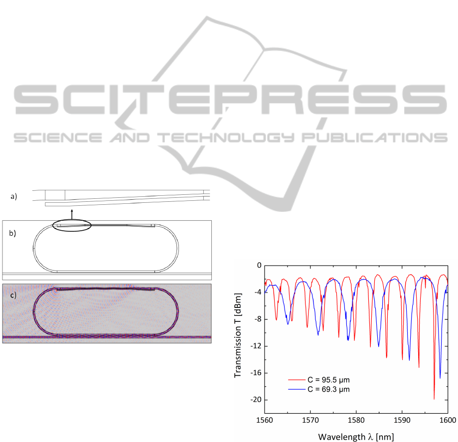
Figure 5 shows the concept of a SOH slot-
waveguide ring resonator without silicon striploads.
The ring is partially slotted in order to obtain higher
Q-factors.
Figure 5: a) Strip-to-slot mode-converter. b) SOH slot-
waveguide ring resonator. c) Optical field distribution of
the SOH slot-waveguide ring resonator modulator.
5 EXPECTED OUTCOME
5.1 Theoretical Investigations
Theoretical investigations are mainly done in order
to find optimized geometrical parameters for slot-
waveguide structures. Figures of merit such as
field confinement factors and effective nonlinear area
are calculated and published (Steglich et al., 2014;
Steglich et al., 2015a; Steglich et al., 2015b). Fur-
ther simulations will concentrate on design improve-
ments of strip-to-slot mode-converter in order to de-
crease optical losses.
5.2 Device Fabrication
First SOH modulator concepts are transferred to
an appropriate design and fabricated at the IHP
in a 0.13 µm SiGe BiCMOS production line us-
ing 200 mm SOI wafers and 248 nm DUV lithog-
raphy. For instance, SOH slot-waveguide ring res-
onator modulators with a circumferences of 69.3 µm
and 95.5 µm have been fabricated. The transmis-
sion spectrum is shown in Figure 6. Measured
Q-factor, Full-Width-Half-Maximum (FWHM) and
Free-Spectrum-Range (FSR) of three fabricated mi-
cro slot-waveguide ring resonators are listed in Ta-
ble 1. The stated slot widths are not yet confirmed
by the results of a focus ion beam and may there-
fore slightly differ from the expected value. We ex-
pect a Q-factor of about 29000 which is almost six
times higher compared to state of the art SOH slot-
waveguide ring resonator modulators (Gould et al.,
2011). Future work will concentrate on the deposi-
tion of organic materials from the vacuum instead of
spin-coating. The advantage is the possibility to fill-
out trenches with high aspect ratios at the backside of
SOI wafers. This is necessary to open slot-waveguide
structures without the destruction of the BEOL and
in order to deposit organic materials without covering
the metal electrodes.
Figure 6: Transmission of SOH slot-waveguide ring res-
onator resonators with different slot widths fabricated with
a 248 nm DUV lithography.
ConceptsandDesignofNovelIntegratedPhotonicDevicesbasedonSilicon-organicHybridTechnology
59

Table 1: Characteristics of the fabricated SOH slot-waveguide ring resonator resonators.
circumference [µm] slot width [nm] center wavelength [nm] FWHM [nm] FSR [nm] Q-factor
69.3 130 1598.03 0.31465 6.7 5079
69.3 150 1586.5 0.47424 7 3345
95.5 130 1597.05 0.05497 3.3 29054
95.5 110 1573.58 0,01567 3.4 100420
6 STAGE OF THE RESEARCH
Three year of research will be needed. The first year
has been completed successfully. This period in-
cluded a first concept development and optimization
through numerical simulations as well as a first de-
sign realization. Figure of merits such as field con-
finement factors and nonlinear effective areas of slot-
waveguide structures are calculated and presented at
the EOSAM 2014 in Berlin as an oral presentation
(Steglich et al., 2014). Further simulation results
and SOI slot-waveguide design trade-offs will be pre-
sented at the PHOTOPTICS 2015 in Berlin as FULL
paper with an oral presentation (Steglich et al., 2015a)
and at the CLEO/Europe 2015 in Munich (Steglich
et al., 2015b). Beside theoretical investigations, first
electro-optical modulators have been fabricated with
a SiGe BiCMOS pilot line at the IHP. We expect to
demonstrate our first measurements on SOH modula-
tor during the next few months.
ACKNOWLEDGEMENTS
The authors would like to thank the German Federal
Ministry of Education and Research (BMBF) for the
financial support under contract no. 03FH086PX2,
the University of Applied Sciences Wildau (THWi),
Germany, and the Ministry of Science, Technology
and Culture of the federal state Brandenburg, Ger-
many, for financial support. The authors would also
like to thank Fr. Nanni, P. Prosposito, F. De Matteis,
and R. De Angelis from the University of Rome Tor
Vergata, Italy, St. Meister and A. Al-Saadi from the
Technical University Berlin, Germany, and L. Zim-
mermann, D. Knoll, D. Stolarek, J. Katzer, St. Lis-
chke, H. Silz, B. Tillack and W. Mehr from the In-
stitute of High-Performance Microelectronics (IHP),
Germany, for their encouragement and support in the
framework of the Joint-Lab IHP-THWi.
REFERENCES
Agrawal, G. (2012). Nonlinear Fiber Optics. Academic
Press, 5 edition.
Almeida, V. R., Xu, Q., Barrios, C. A., and Lipson, M.
(2004). Guiding and confining light in void nanos-
tructure. Opt. Lett., 29(11):1209–1211.
Barrios, C. A., Gylfason, K. B., S
´
anchez, B., Griol,
A., Sohlstr
¨
om, H., Holgado, M., and Casquel, R.
(2007). Slot-waveguide biochemical sensor. Opt.
Lett., 32(21):3080–3082.
Claes, T., Molera, J., De Vos, K., Schachtb, E., Baets, R.,
and Bienstman, P. (2009). Label-free biosensing with
a slot-waveguide-based ring resonator in silicon on in-
sulator. Photonics Journal, IEEE, 1(3):197–204.
Dalton, L. R., Sullivan, P. A., and Bale, D. H. (2010). Elec-
tric field poled organic electro-optic materials: State
of the art and future prospects. Chemical Reviews,
110(1):25–55.
Dell’Olio, F. and Passaro, V. M. (2007). Optical sensing
by optimized silicon slot waveguides. Opt. Express,
15(8):4977–4993.
Feng, N.-N., Michel, J., and Kimerling, L. (2006). Optical
field concentration in low-index waveguides. Quan-
tum Electronics, IEEE Journal of, 42(9):885–890.
Gould, M., Baehr-Jones, T., Ding, R., Huang, S., Luo,
J., Jen, A. K.-Y., Fedeli, J.-M., Fournier, M., and
Hochberg, M. (2011). Silicon-polymer hybrid slot
waveguide ring-resonator modulator. Opt. Express,
19(5):3952–3961.
Koos, C., Jacome, L., Poulton, C., Leuthold, J., and Freude,
W. (2007). Nonlinear silicon-on-insulator waveg-
uides for all-optical signal processing. Opt. Express,
15(10):5976–5990.
Korn, D., Jazbinsek, M., Palmer, R., Baier, M., Alloatti, L.,
Yu, H., Bogaerts, W., Lepage, G., Verheyen, P., Absil,
P., Guenter, P., Koos, C., Freude, W., and Leuthold,
J. (2014). Electro-optic organic crystal silicon high-
speed modulator. Photonics Journal, IEEE, 6(2):1–9.
Korn, D., Palmer, R., Yu, H., Schindler, P. C., Alloatti,
L., Baier, M., Schmogrow, R., Bogaerts, W., Sel-
varaja, S. K., Lepage, G., Pantouvaki, M., Wouters,
J. M., Verheyen, P., Campenhout, J. V., Chen, B.,
Baets, R., Absil, P., Dinu, R., Koos, C., Freude,
W., and Leuthold, J. (2013). Silicon-organic hybrid
(soh) iq modulator using the linear electro-optic effect
for transmitting 16qam at 112 gbit/s. Opt. Express,
21(11):13219–13227.
Leuthold, J., Koos, C., Freude, W., Alloatti, L., Palmer, R.,
Korn, D., Pfeifle, J., Lauermann, M., Dinu, R., Wehrli,
PHOTOPTICS2015-DoctoralConsortium
60

S., et al. (2013). Silicon-organic hybrid electro-optical
devices. Selected Topics in Quantum Electronics,
IEEE Journal of, 19(6):3401413–3401413.
Liu, Y., Baehr-Jones, T., Li, J., Pomerene, A., and
Hochberg, M. (2011). Efficient strip to strip-loaded
slot mode converter in silicon-on-insulator. Photonics
Technology Letters, IEEE, 23(20):1496–1498.
Palik, E. D. (1997). Handbook of Optical Constants of
Solids. Academic Press, 1 edition.
Palmer, R., Alloatti, L., Korn, D., Heni, W., Schindler,
P., Bolten, J., Karl, M., Waldow, M., Wahlbrink, T.,
Freude, W., Koos, C., and Leuthold, J. (2013a). Low-
loss silicon strip-to-slot mode converters. Photonics
Journal, IEEE, 5(1):2200409–2200409.
Palmer, R., Alloatti, L., Korn, D., Schindler, P., Baier,
M., Bolten, J., Wahlbrink, T., Waldow, M., Dinu, R.,
Freude, W., Koos, C., and Leuthold, J. (2013b). Low
power mach-zehnder modulator in silicon-organic hy-
brid technology. Photonics Technology Letters, IEEE,
25(13):1226–1229.
Palmer, R., Alloatti, L., Korn, D., Schindler, P., Schmogrow,
R., Heni, W., Koenig, S., Bolten, J., Wahlbrink, T.,
Waldow, M., Yu, H., Bogaerts, W., Verheyen, P., Lep-
age, G., Pantouvaki, M., Van Campenhout, J., Absil,
P., Dinu, R., Freude, W., Koos, C., and Leuthold, J.
(2013c). Silicon-organic hybrid mzi modulator gener-
ating ook, bpsk and 8-ask signals for up to 84 gbit/s.
Photonics Journal, IEEE, 5(2):6600907–6600907.
Palmer, R., Koeber, S., Woessner, M., Elder, D. L., Heni,
W., Korn, D., Yu, H., Lauermann, M., Bogaerts, W.,
Dalton, L. R., Freude, W., Leuthold, J., and Koos, C.
(2014). High-speed silicon-organic hybrid (soh) mod-
ulators with 230 pm/v electro-optic coefficient using
advanced materials. In Optical Fiber Communication
Conference, page M3G.4. Optical Society of America.
Robinson, J. T., Preston, K., Painter, O., and Lip-
son, M. (2008). First-principle derivation of gain
in high-index-contrast waveguides. Opt. Express,
16(21):16659–16669.
Steglich, P., Padilla Michel, Y., Villringer, C., D
¨
umecke, S.,
Casalboni, M., and Schrader, S. (2014). Numerical
simulation of silicon-organic hybrid slot-waveguides.
European Optical Society Annual Meeting (EOSAM).
Steglich, P., Padilla Michel, Y., Villringer, C., D
¨
umecke, S.,
Casalboni, M., and Schrader, S. (2015a). Silicon-on-
insulator slot-waveguide design trade-offs. PHOTOP-
TICS.
Steglich, P., Villringer, C., D
¨
umecke, S., Padilla Michel, Y.,
Casalboni, M., and Schrader, S. (2015b). Investigation
of optical field confinement of silicon-on-insulator
slot-waveguides for integrated electro-optical modu-
lator. CLEO.
Tsang, H., Wong, C., Liang, T., Day, I., Roberts, S., Harpin,
A., Drake, J., and Asghari, M. (2002). Optical dis-
persion, two-photon absorption and self-phase mod-
ulation in silicon waveguides at 1.5 µm wavelength.
Applied Physics Letters, 80(3):416–418.
Vivien, L. and Pavesi, L., editors (2013). Handbook of Sili-
con Photonics. CRC Press, 0 edition.
Weimann, C., Schindler, P. C., Palmer, R., Wolf, S., Bekele,
D., Korn, D., Pfeifle, J., Koeber, S., Schmogrow, R.,
Alloatti, L., Elder, D., Yu, H., Bogaerts, W., Dal-
ton, L. R., Freude, W., Leuthold, J., and Koos, C.
(2014). Silicon-organic hybrid (soh) frequency comb
sources for terabit/s data transmission. Opt. Express,
22(3):3629–3637.
ConceptsandDesignofNovelIntegratedPhotonicDevicesbasedonSilicon-organicHybridTechnology
61
