
Modeling and Simulation of Logic Gates using DEVS
Maamar Hamri
1,2,3,4
and Nesrine Driouche
5
1
Aix Marseille Universit
´
e, LSIS UMR 7296, 13397, Marseille, France
2
CNRS, LSIS UMR 7296, 13397, Marseille, France
3
ENSAM, LSIS UMR 7296, 13397, Marseille, France
4
Universit
´
e de Toulon, LSIS UMR 7296, 13397, Marseille, France
5
Independant Software Researcher, Marseille, France
Keywords:
Logic Gates, DEVS, Modeling and Simulation, Performances.
Abstract:
Discrete event simulation becomes popular more and more and was applied successfully in many fields:
medicine, robotics, etc. One of this field is digital circuits for which boolean logics is the basis of compu-
tation by designing logic gates. However such a paradigm does not consider the time basis. Consequently, the
boolean logic paradigm can not design and simulate delays of circuits and stamped explicitly computations.
In this paper, we propose to combine the boolean logic paradigm and Discrete EVent system Specification
(DEVS) formalism for modeling and simulation logic gates. Using this approach, we are able to design com-
plex network of logic gates by reusing and coupling basic ones and to analyze behavior through time.
1 INTRODUCTION
Digital circuits is viewed at conceptual level as net-
works of logic gates on which verification and test are
possible. A basic logic gate has multiple inputs and
only one output computed according to a truth table
or a logic statement. Complex logic gates are built
from basic ones and coupled using connectors. How-
ever, the boolean logic paradigm, alone, is not able to
consider delay occurring in digital circuits due to used
hardware materials (transistors) for the design.
Languages like VHDL, Verilog, etc. are well-
known for designing logic gates, and checking for-
mally and by simulation the behavior (Brown and
Vranesic, 2003)(Palnitkar, 2003). However, we hope
highlight the power of DEVS to desgin such gates.
Some works from DEVS focused on designing
logic gates. (Tendeloo and Vangheluwe, 2013) pro-
posed an apporach to translate logisim
c
models in
DEVS with keeping logisim semantics. This ap-
proach showed that DEVS simulator performs sim-
ulations of digital circuits more faster than logisim.
(Cappochi et al., ) proposed an approach to trans-
form VHDL models to parallel-DEVS with an ex-
ample based on an8-bit register. However, the use
of a synchronization model in order to schedule ac-
tive processes slows down the simulation due to the
additional exchanged messages inside the simula-
tor. (Hamri et al., 2015) proposed an approach to
design logic gates in GDEVS (Generalize Discrete
EVent system Specification (Giambiasi et al., 2000))
in which input and output signals are linear segments
instead of constants to represent accurately signals
and state changes.
However, in this work, we propose a library of
DEVS components built from the timed boolean logic
paradigm to design logic gates, avoiding the use of
an additional semantics from other paradigms like in
(Tendeloo and Vangheluwe, 2013). So, we show that
DEVS is able to design such gates using its own se-
mantics and tools. On the other hand, designing in-
put and output signals with constants (boolean 0 and
1) and states with constant piece-wise, even if such a
design is less accurate than that proposed in (Hamri
et al., 2015), allows comparisons with other tool like
VHDL, Verilog, etc. using the same definitions on
input and output signal, state changes, etc.
2 BACKGROUND
DEVS is one of the popular discrete event formalisms
proposed in 70´s by Zeigler (Zeigler, 1976). The
DEVS M&S framework separates clearly modeling
212
Hamri M. and Driouche N..
Modeling and Simulation of Logic Gates using DEVS.
DOI: 10.5220/0005567202120218
In Proceedings of the 5th International Conference on Simulation and Modeling Methodologies, Technologies and Applications (SIMULTECH-2015),
pages 212-218
ISBN: 978-989-758-120-5
Copyright
c
2015 SCITEPRESS (Science and Technology Publications, Lda.)

concerns from simulation ones. In fact, DEVS ab-
stract simulator is useful to produce the behaviors of
any model that respects the DEVS definitions. On
the other hand, DEVS models are reused and coupled
among them to make new DEVS models. Many re-
search and practical works were realized around this
formalism thanks to its powerful expressiveness. This
formalism has many extensions: GDEVS (Giambiasi
et al., 2000), parallel-DEVS(Chow, 1996), etc. and
applications in different fields: forest fire spread (Hu
et al., 2012), biological systems (Uhrmacher et al.,
2005), etc.
2.1 DEVS Atomic Formalism
According to the literature on DEVS (Zeigler et al.,
2000), the specification of a discrete event model is a
structure, M, given by:
M = (X, S, Y, δ
int
, δ
ext
, λ, ta), where X is the set of
the external input events, S the set of the sequential
states, Y the set of the output events, δ
int
is the inter-
nal transition function which defines the state changes
caused by internal events, δ
ext
is the external transi-
tion function which specifies the state changes due to
external events, λ is the output function, and the func-
tion ta : S → R
+
∪ ∞ represents the maximum length
or the lifetime of a state. Thus, for a given state s,
ta(s) represents the time during which the model will
remain in state s if no external event occurs.
2.2 DEVS Coupled Formalism
DEVS promotes modular modeling to reduce the
complexity of the system to describe. The DEVS
coupled structure allows formalizing the modeled
system in a set of inter-connected and reused compo-
nents.
MC = (X
MC
, Y
MC
, D
MC
, M
d|d∈D
, EIC, EOC, IC, Select),
where
• X
MC
: set of external events.
• Y
MC
: set of output events.
• D
MC
: set of components names.
• M
d
: DEVS model named d.
• EIC: External Input Coupling relations.
• EOC: External Output Coupling relations.
• IC: Internal Coupling relations.
• Select: defines a priority between simultaneous
events intended for different components.
This formalism is proved by the closure under
coupling property, which shows that a DEVS coupled
model is a DEVS atomic one.
2.3 DEVS Simulator
The DEVS abstract simulator (see Figure 1) consists
of a root-coordinator, which manages the simulation
time, sub-coordinators which dispatch messages ac-
cording to the specific couplings of the coupled model
that attempt to simulate and basic simulators related
to atomic models. Each process behaves according
to the received messages from parent and child pro-
cesses.
Figure 1: DEVS abstract hierarchical simulator.
The classic structure of DEVS simulator is a hi-
erarchical one, represented as a tree in which at top
level is the root followed by the sub-coordinators cre-
ated from DEVS coupled structure; then, at low level
there are basic simulators related directly to the cor-
responding DEVS atomic models in order to execute
the different functions δ
int
, δ
ext
, λ and ta. Figure 1 il-
lustrates this structure and messages transiting from a
process to another.
2.4 Simulators of Logic Gates
Designing digital circuits is based essentially on in-
terconnected logic gates. These gates are a compo-
sition of the basic gates and, or, and not in order to
express the functional view of the circuits, and delay
blocks to express the amount of times that a digital
pulse crosses a physical device. A digital pulse is a
series of waves reproduced periodically, i.e, a set of
rise and fall events well stamped according to a global
clock. In addition, such a pulse is limited to two volt-
age values (0 and 5 volts) which corresponds to 0 and
1 in logics.
Many software are dedicated to M&S logic gate
like simulink
c
, VHDL
c
, Verilog
c
, logic gate
simulator
c
, etc. that we can classify them into two
main categories: educational and professional. Both
of them use the M&S concepts noted above, modu-
larity, reusing, connectors, etc. Educational software
ModelingandSimulationofLogicGatesusingDEVS
213

focus on learning simple rules on logics (truth tables)
and how new components can be designed. However,
professional software provides advanced services like
formal verification of circuits, stochastic simulation,
etc. Afterwards, we retain Verilog for its simple use
and for which the language is close to programming
language C.
2.5 Logic Gates in Verilog
Verilog standardized as IEEE1364, is a hardware de-
scription language used to model and simulate digi-
tal circuits (Wikipedia, 2015). It provides abstraction
and reusing of primitives, blocks and modules to de-
sign new modules in hierarchical way. Many works
showed the power of Verilog to design logic gates.
In addition other works proposed methods to fix bugs
and check timing conditions such as flip-flop set-up,
hold violation, etc.
Verilog proposes different designs and implemen-
tation for logic gates. The modeler may design basic
gates with or without ports. Time delay of logic gates
is by default zero. However, the modeler may define a
non-zero value for the pure delay (constructor delay)
by using the operator #delay. Note that other delays
can be used like fall-rise and min-max delays.
In the following the Verilog code of the gates not
and and :
//create a not gate
module logic_not (b, a);
// declare port signals
//b is output, a is input
output b;
input a;
not #1 n1(b,a);
endmodule
//create an and gate
module logic_and (c, a, b);
// declare port signals
output c;
input a,b;
//c is output, a, b are inputs
and #1 and1(c,a,b);
endmodule
From such basic modules, composite ones are
built and for which statements may be added.
3 MODELING LOGIC GATES IN
DEVS
Modeling logic gates in DEVS is easy thanks to its
modeling concepts that ensures modularity, reuse, ex-
plicit time representation, etc. The modeler may en-
close basic gates in DEVS atomic components then
reuse them to design new components (nand, nor,
f lip − f lop, etc.) by coupling inports and outports
of each reused components and the component under
design according to DEVS coupled specification.
At low level, the function view of basic logic gates
and, or and not, i.e, how the output is computed from
present inputs are logically described using the func-
tions of DEVS atomic: δ
ext
(), δ
int
(), and λ(). In
fact δ
ext
() allows storing the inputs of the considered
gate which schedules, then, an output according to
the specified delay by calling the function ta(). Af-
terwards, the function δ
int
() allows the logic gate to
change state from an active one to a passive one (wait-
ing for a new input) enabling the sending of the com-
puted output of the function λ().
Let us consider the logic gate and with two
inports and one output, and a pure delay d = 1
nanosecond (ns):
gate : and
parameter : d = 1 ns;
inports : in
0
, in
1
; outports : out;
variables states : bool a, b, y;
real sigma;
δ
ext
(s, e, in
0
): a = in
0
;
y = min(a, b);
sigma = d;
δ
ext
(s, e, in
1
): b = in
1
;
y = min(a, b);
sigma = d;
δ
int
(): sigma= infinity;
output(): send (out = y);
ta(): return sigma ;
endgate
Note that, in our design for DEVS logic gates, we
prefer the use of logic statements instead of truth ta-
bles to compute the output of each logic gate, in order
to avoid a series of test to do that. In fact, we consider
the following simple equations:
not(a) =!a (1)
and = min(a, b) (2)
or = max(a, b) (3)
These elementary gates designed in DEVS are the
basis of designing other well-known logic gate like
nand, nor, xor, etc. The modeler reuses the necessary
components and couples them through the inports and
outports to make the final component.
Let us consider the gate nand which consists of
the gates and and not coupled in series. The following
program describes the gate nand in DEVS:
gate: nand
inports: in0, in1;
outports: out;
SIMULTECH2015-5thInternationalConferenceonSimulationandModelingMethodologies,Technologiesand
Applications
214

components: and, not;
couplings: couple(nand, in0, and, in0);
couple(nand, in1, and, in1);
couple(and, out, not, in);
couple(not, out, nand, out);
endgate
Note that the modeler may define its own libraries
to store designed components and may reuse them in
hierarchical way furthermore. Moreover, some com-
ponents may be designed differently. For example,
the gate and with multiple inports may be designed
as a composite gate based on a set of n gates and in
series (see Figure 2).
Figure 2: The composite gate and
4
.
On the other hand, an elementary gate may be de-
signed for such a gate and with n inports by using an
algebraic function shown by the equation 4.
and
n
= min(a
0
, a
1
, . . . , a
n
) (4)
By analogy, the gate or with multiple inports may
be designed in two different ways: by coupling a set
of gates or in series; or by designing a new gate or
n
where n is the number of inports; and the computation
of the corresponding output is based on the following
equation 5:
or
n
= max(a
0
, a
1
, . . . , a
n
) (5)
These two designs are not really disconnected. In
fact these two designs allow getting equivalent mod-
els. Knowing that the closure under coupling prop-
erty of DEVS shows that each coupled model has an
equivalent in DEVS atomic. Consequently, our two
elementary gates and
n
and or
n
are obviously the re-
sult of the put in flat of the composite gates and and
or with multiple inports.
Let us consider the gate composite and
n
with mul-
tiple inports. According to the closure under coupling
property, we are able to design a basic gate in DEVS
atomic as follows:
gate : and
parameter : d =× delay
i
;
// inports of the gate composite
inputs : in
0
, in
1
, ..., in
n
;
// outport of the gate composite
outputs : out;
variables states :
bool ×(a
i
, b
i
) i = 1..n
real sigma
i
i=1..n;
δ
ext
(s, e, in
i
):
δ
i,ext
(s, e, in
i
); i = 1..n
δ
1,ext
(s, e, in
0
); i = 0
δ
int
(): δ
i,int
();
δ
i+1,ext
(s, 0, output
i
) i = 1..n-1
output():
output
n
;
ta():
sigma = min(sigma
1
, sigma
2
, ... ,sigma
n
)
return sigma ;
endgate
By rewriting the functions δ
ext
and δ
int
, we obtain:
δ
ext
(s, e, in
i
): b
i
= in
i
i = 1..n
sigma
i
= delay
(if i = 0 then a
0
= in
0
sigma
1
= delay)
δ
int
() : sigma
i
= ∞
a
i+1
= min(a
i
, b
i
)
the output of the gate and
i+1
is:
λ() : min(a
i+1
, b
i+1
) →
min(min(a
i
, b
i
), b
i+1
) replace a
i+1
= min(a
i
, b
i
) →
min(a
i
, b
i
, b
i+1
) the function min is associative
by expansing, the output of the next gate and
i+2
, is:
λ() : min(a
i+2
, b
i+2
) →
min(δ
i+2,ext
(s, e, λ
i+1
), b
i+2
) →
min(min(a
i+1
, b
i+1
), b
i+2
) →
min(min(min(a
i
, b
i
), b
i+1
), b
i+2
) →
min(a
i
, b
i
, b
i+1
, b
i+2
)
by recurrence, we have for the gate and
n
:
λ
n
: min(a
1
, b
1
, . . . , b
n−1
, b
n
)
remains to rename the variables a
1
to a
0
and each b
i
to a
i
, finally we obtain:
λ
n
: min(a
0
, a
1
, . . . , a
n
)
which corresponds to the output of the gate basic
and
n
.
By using the same proof we can deduce also that
the gate composite or
n
may be designed with two dif-
ferent and equivalent designs.
4 DESIGNING LOGIC GATES IN
DEVS SIMULATOR
Our logic gate components support any DEVS simu-
lator (adevs, devsjava, etc.) but we use our own DEVS
simulator developed in Java to design these compo-
nents, experiment it and show that it produce the right
outputs at right times. The design of any composite
logic gate follows the class diagram shown on Fig-
ure 3. The modeler should extend for each new log-
ical gate the class DEVSCoupled, define inports and
ModelingandSimulationofLogicGatesusingDEVS
215
outports, declare reused logical gates, and then define
the coupling over them. Once the final logic gate is
ready, the modeler may couple its inports with pulse
generator component to emulate an input signal or init
a scheduler of input events, then he can start the sim-
ulation.
DEVSModel
Not
And
NorNand
DEVSAtomicDEVSCoupled
Or
+selectPriority()
Figure 3: Object design of logic gates in DEVS.
Now let us consider the well-known logic gate rs-
latch defined by the following equation:
Q
0
= QR + RS (6)
where S, R are the inputs, Q is the present output and
Q
0
is the next output.
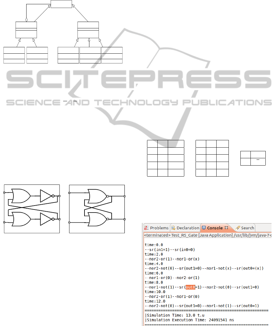
In DEVS, such a gate may be designed by four
elementary gates: two or and two not; or in hierar-
chical way through two composite gates nor. In order
to favour modularity, reusability and hierarchical de-
sign, we model the sr − latch by using two gates nor
coupled correctly, even if the design based on elemen-
tary gates remains valid. The two possible designs are
shown on Figure 4.
(a) Non-hierarchical rs-
latch.
(b) Hierarchical rs-latch.
Figure 4: Modeling a rs-latch in DEVS.
A piece of code in our DEVS simulator imple-
menting the gate sr-latch according to a hierarchical
design, is shown below:
public class SR extends DEVSCoupled {
Nor nor1, nor2;
Port in0, in1, out0, out1;
public SR(){
super();
nor1 = new Nor("nor1");
nor2 = new Nor("nor2");
in0 = new Port("in0");
in1 = new Port("in1");
out0 = new Port("out0");
out1 = new Port("out1");
this.addInPort(in0);
this.addInPort(in1);
this.addOutPort(out0);
this.addOutPort(out1);
this.SubModels.add(this.nor1);
this.SubModels.add(this.nor2);
//sr (in0) --> nor1 (in0)
this.addEIC(this.getInPorts().get(0),
this.nor1.getInPorts().get(0));
...
}
However, to start simulation of the gate sr-latch,
the modeler should define its init state. If this state
is clearly known, the outputs of this gate belong to
{0,1}, but in some cases such a state may not be
known because the outputs, that are also inputs, are
not yet computed (cf. equation 6 and Figure 4). Con-
sequently, a some interval time is necessary to com-
pute the outputs and then set state variables of the init
state. For that, we add a new behavior for each ele-
mentary gate to take into account the unknown state x
according to the truth tables below:
Table 1: Truth tables of and, or and not with unknown input.
a b and
x 1 x
1 x x
x 0 0
0 x 0
a b or
x 1 x
1 x x
x 0 0
0 x 0
a not
x x
Now, let us consider the inputs s = 0 and r = 1 at
time t = 0. The produced sr-latch outputs displayed
on Figure 5, shows that our design using our simulator
produces the right output events according to sr-latch
boolean function at right time.
Figure 5: Simulation of the rs-latch in DEVS.
SIMULTECH2015-5thInternationalConferenceonSimulationandModelingMethodologies,Technologiesand
Applications
216

Moreover, the gate sr-latch may produce illegal
output when s = r = 1. Our elementary gates respects
DEVS encapsulation principle, so access to state vari-
ables are limited to elementary gate where those vari-
ables are declared. In order to avoid a not allowed
state for the gate sr-latch, we may couple its output
with a monitor component to forbidden undesirable
outputs by checking the assertion out
0
6= out
1
each
time an output is sent out through the port out
0
or out
1
.
However, this solution even if it avoids undesirable
outputs but it leads the sr-latch transitioning to an un-
desirable state. It is better to avoid undesirable inputs
than handle undesirable outputs. By adding a monitor
component handling the inputs s and r, we guaran-
tee that the sr-latch transition to a desirable state and
send out desirable outputs. As conclusion, designing
a valid sr-latch consists of using an additional compo-
nent that checks whether the inputs are desirable and
a gate sr-latch that design its logic function. This is
an issue to handle desirable inputs for any logic gate.
5 PERFORMANCE
COMPARISON
In order to show that DEVS is able to make simula-
tions of logic gate as fast as verilog, we firstly give
the simulation execution times of basic logic gates
and, or, not, nand and nor in both adevs-2.8.1 and
verilog-0.9.7. The input data simulation are identical
for both simulations: same delay for all atomic gates
and same input pulses; the simulation time is 4000
u.t (units of time). These simulations are carried out
on personal computer DELL with CPU Intel
c
Core2
Duo CPU E8400 - 3.00GHz × 2 where is set Ubuntu
14.0.4. The results are shown on Table 2.
Table 2: Execution time means of basic logic gates in mil-
liseconds.
and or not nand nor
adevs 16.0 15.6 9.2 24.8 17.2
verilog 23.6 22.0 18.0 24.0 23.2
By looking to results shown on Table 2, glob-
ally, the M&S of logic gates using adevs provides a
concrete gain on execution time. So, DEVS simula-
tion of logic gates is able to provide quick simula-
tions as such as those provided by well-known tools
in this field like verilog. In fact, the gate not designed
in DEVS is distinguished by a small execution time
comparing to other gates. The gate not has only one
inport, so it avoids the function δ
ext
to use the condi-
tional statement if then to determine on which port
the gate has received an event. This fact explains
what the gates and and or have considerable execu-
tion time for the same simulation data. These gates
hold two inports and they should check on which port
the event was received in order to update the right
state variable and compute correctly the output. The
composite gates nand and nor have the higher execu-
tion times due to fact that they involves each one two
internal gates {and, not} and {or, not} respectively. It
is quite that these composite gates present such exe-
cution times.
Now let us consider both design in adevs and ver-
ilog, the execution time of simulating basic gates and,
or and not with adevs are less than those in verilog.
However, the execution time of gates nand and nor
in adevs and verilog are close. This lost on speed of
adevs simulation is due to the architecture of DEVS
simulation which introduces additional processes (co-
ordinator) to simulate composite logic gates. Some-
one may believe that adevs loses on speed each time,
for the simulation of more complex composite gates.
For that we can use new architectures enhancing sim-
ulation process like those proposed by (Kim et al.,
2000) and (Franceschini and Bisgambiglia, 2014) to
reduce intermediary processes, and so the messages
will cross short paths. What this suggests that adevs
and DEVS simulator in C++ may provide interest-
ing simulation execution times of logic gate close to
Verolig.
Therefore DEVS as a discrete event formalism
and its simulation software could compare with other
software well-known and specialized in the field of
logic gate application.
6 CONCLUSION
In this paper, we proposed a modular and hierarchi-
cal approach to design logic gates in DEVS. We used
a simple language based on DEVS to design both
atomic and composite gates. In this approach, we
introduced logic statements well-known in logics to
compute outputs of logic gates and the time basis
to delay outputs with regard to inputs. In addition,
we were led to re-design the behavior of basic gates
in order to take into account the unknown state of
logic latches that occurs at initialization of simulation.
Note that our approach allows filtering inputs to avoid
the non-allowed state for these latches by composi-
tion, i.e., by a simple DEVS component that sends
out to latches only acceptable inputs. Recall that, the
adevs and verilog simulations carried out for differ-
ent logic gates provide execution times close for each
other.
Moreover, the approach still opens to take into
ModelingandSimulationofLogicGatesusingDEVS
217

account other types of delay: rise-fall, min-max,
etc. which involve a simulation semantics different.
DEVS and its extensions are able to deal with such de-
lays; this point will constitute one of our future works.
In addition, we will tackle the synthesis of composite
logic gates (for example, three gates not in series is
simplified to one gate not) and put in flat the network
of gates automatically.
REFERENCES
Brown, S. and Vranesic, Z. (2003). Fundamentals of Digital
Logic with Verilog Design. Addison-Wesley Longman
Publishing Co., 1st edition.
Cappochi, L., Bernardi, F., Federici, D., and Bisgambiglia,
P.-A. Transformation of vhdl descriptions into devs
models for fault modeling and simulation, october 5-
8, 2003. In International Conference on Systems, Man
and Cybernetics, pages 1205–1210, Washinton DC
USA. IEEE, 2003.
Chow, A. C. (1996). Parallel devs: a parallel, hierarchi-
cal, modular modeling formalism and its distributed
simulator. Transactions of the Society for Computer
Simulation International, 13:55–67.
Franceschini, R. and Bisgambiglia, P.-A. (2014). Decentral-
ized approach for efficient simulation of devs models.
In Heidelberg, S. B., editor, FIP WG 5.7 International
Conference, APMS 2014, Ajaccio, France, September
20-24, 2014, Proceedings, Part III, pages 336–343,
Ajaccio, France.
Giambiasi, N., Escud
´
e, B., and Ghosh, S. (2000). GDEVS:
A generalized discrete event specification for accurate
modeling of dynamic systems. Simulation: Transac-
tions of the Society for Modeling and Simulation In-
ternational, 17(3):120–134.
Hamri, M., Giambiasi, N., and Naamane, A. (2015). Gener-
alized discrete events for accurate modeling and sim-
ulation of logic gates. PartIII:257–272.
Hu, X., Sun, Y., and Ntaimo, L. (2012). Devs-fire: de-
sign and application of formal discrete event wildfire
spread and suppression models. Simulation: Transac-
tions of the Society for Modeling and Simulation In-
ternational, 88(3):259–279.
Kim, K., Kang, W., Sagong, B., and Seo, H. (2000).
Efficient distributed simulation of hierarchical devs
models: Transforming model structure into a non-
hierarchical one. In SCS, editor, 33rd Annual Simu-
lation Symposium, pages 227–188.
Palnitkar, S. (2003). Verilog HDL: A Guide to Digital De-
sign and Synthesis, Second Edition. Addison-Wesley
Longman Publishing Co., 2nd edition.
Tendeloo, Y. V. and Vangheluwe, H. (2013). Logisim
to devs translation. In Proceedings of the 2013
IEEE/ACM 17th International Symposium on Dis-
tributed Simulation and Real Time Application, DS-
RT´13, pages 13–20, San Diego, CA, USA. IEEE
Computer Society Washington, DC, USA2013.
Uhrmacher, A. M., Degenring, D., and Zeigler, B. (2005).
Discrete event multi-level models for systems biology.
3380:66–89.
Wikipedia (2015). http://en.wikipedia.org/wiki/verilog.
Zeigler, B. P. (1976). Theory of Modeling and Simulation.
Fisrt edition - Academic Press.
Zeigler, B. P., Praehofer, H., and Kim, T. G. (2000). Theory
of Modeling and Simulation. Academic Press.
SIMULTECH2015-5thInternationalConferenceonSimulationandModelingMethodologies,Technologiesand
Applications
218
