
A 71PS-RESOLUTION MULTI-CHANNEL CMOS
TIME-TO-DIGITAL CONVERTER FOR POSITRON EMISSION
TOMOGRAPHY IMAGING APPLICATIONS
Wu Gao
1, 2
, Christine Hu-Guo, Nicolas Ollivier-Henry, Yann Hu
1
Institut Pluridisciplinaire Hubert CURIEN (ULP, CNRS/IN2P3), 67100,Strasbourg, France
Deyuan Gao, Tingcun Wei
2
Aviation Microelectronics Center, Northwestern Polytechnical University, Xi’an, 710072, China
Keywords: Time-to-Digital Converter (TDC), Delay Locked Loop (DLL), Array of DLL’s, Positron Emission
Tomography (PET).
Abstract: This paper presents a high-resolution multi-channel Time-to-Digital Converter (TDC) for Positron Emission
Tomography (PET) imaging system. The TDC using a two-level conversion scheme is proposed for
obtaining high timing resolution. Double 10-bit gray counters are designed for coarse conversion while a
multiphase sampling technology is presented for fine conversion. In order to achieve better timing
resolution with either a faster technology, an array of Delay-locked loops is chosen as a timing generator. A
prototype chip of 3-channel TDC is designed and fabricated in AMS 0.35µm CMOS technology. The area
of the chip is 8.4 mm
2
in size. The measured range of the TDC is 10µs. The time tap is reduced to 71ps with
a reference clock of 100MHz. The differential nonlinearity is ±0.1LSB. The circuits will be extended to 64
channels for small animal PET imaging systems.
1 INTRODUCTION
Positron Emission Tomography (PET), which is a
leading imaging technique for the detection of
cancer, has been demanded for a non-invasive
imaging system for clinical diagnosis by
measurement of the metabolic activity (Mbow et al.,
2007). The physical principle is based on the
detection of gamma radiations resulting from the
disintegration of positrons emitted by the
radiotracer. A pair of 511keV photon generates from
the annihilation of a positron and an electron. The
photons (511keV) are emitted in opposite directions
and both are absorbed by detector module and
converted into an electrical signal. The signal is then
amplified and digitized by a serial of readout
electronics. By taking a large number of coincident
events, many lines can be constructed. An image can
then be reconstructed by employing a tomographic
algorithm on the data (Mbow et al., 2007), (Brian K.
Swann et al., 2004).
The quality of the image is limited both by the
efficiency of the used detectors and system
resolution including spatial resolution and timing
resolution. The improvement of system resolution
pushes the processing requirements on both novel
detectors and the front-end data acquisition system.
Moreover, semiconductor-based scintillators are
being investigated which could lead to a detection
timing resolution below 100ps (Bourrion and Gallin-
Martel, 2006). Such performance requirement is
calling for high-resolution time-measurement
devices for data acquisition and processing system.
A time-to-digital converter (TDC) is one type of an
electronic instrumentation system that is capable of
measuring the time difference between two random
events. The aim of this paper is to develop a 71ps-
resolution multi-channel Time-to-digital converter
(TDC) to measure the time difference of a pair of
511-keV photons for PET imaging reconstruction.
For each channel, the time intervals from the
moment that coincidence event occurs to the time
that the photons are absorbed by detectors will be
measured, registered and converted to digital
171
Gao W., Hu-Guo C., Ollivier-Henry N., Hu Y., Gao D. and Wei T. (2009).
A 71PS-RESOLUTION MULTI-CHANNEL CMOS TIME-TO-DIGITAL CONVERTER FOR POSITRON EMISSION TOMOGRAPHY IMAGING APPLICA-
TIONS.
In Proceedings of the First International Conference on Computer Imaging Theory and Applications, pages 171-176
DOI: 10.5220/0001768601710176
Copyright
c
SciTePress

signals. The measured dynamic range is 10µs.
Several researchers have reported the design of
TDC for PET imaging systems. An integrated
CMOS sub-nanosecond TDC has been developed
under the aid of flash ADC technology. The time
resolution is reported as 312.5ps (Brian K. Swann et
al., 2004). In addition, a 224ps-resolution TDC
based on DLL technology was reported for liquid
Xenon PET (Bourrion and Gallin-Martel, 2006). The
prototype chip of such TDC included a single DLL
with 128 delay cells. It was difficult to deal with the
mismatch of long-chain delay cells. For obtaining
smaller time resolution, a new architecture based on
a hierarchical delay processing structure was
proposed for next generation PET imaging (Yousif
and Haslettl, 2007). A prototype chip was fabricated
in 0.13µm CMOS process and ran at a clock of
500MHz. Although high resolution was obtained, a
faster technology was needed due to the high-
frequency clock utilized in the chip.
Few studies have been done on development of a
TDC that a better resolution obtained by using either
a faster technology for PET imaging applications.
However, a two-level conversion scheme based on
an array of DLLs is a good solution for this
challenge. The original proposals of TDC based on
array of DLLs have been published in (Christiansen,
1996), (Mota and Christiansen, 1998). A resolution
of 89.3ps was realized with a clock frequency of
80MHz (Mota and Christiansen, 1998). In this
paper, we present the design of a TDC based-on an
array of low-jitter DLLs for PET imaging system.
The results agree with the design of TDC’s in
(Christiansen, 1996) and (Mota and Christiansen,
1998). The better results are achieved because low-
jitter DLLs are employed and the relatively
advanced CMOS technology (0.35µm) is utilized.
The resolution of 71ps with a clock frequency of
100MHz is obtained from our prototype chip.
In Section 2 of this paper, the principle of
measurement and proposed architecture are
described. In Section 3, the description of circuits is
given. In Section 4, a prototype chip of TDC and
experimental results are described. Section 5
concludes the paper.
2 OPERATIONAL PRINCIPLE
AND PROPOSED
ARCHITECTURE
TDC systems are designed to measure the time
interval from START to STOP signal. For large time
interval, a counter is employed to counter numbers
when a reference clock is used. The measured time
equates to the counted number multiple by the
period of the clock. The resolution of TDC is
depended on the period of reference clock. If smaller
time tap is needed, a high-frequency clock needs to
be employed. Another solution is two-level
conversion scheme. The counter is employed for
coarse conversion and a multiphase sampling
technology is proposed for fine conversion. The
multiphase generators are designed to generate
multiphase delayed in one period of the reference
clock. The state of multiphase will be asserted,
registered and converted to binary codes.
A delay-locked loop (DLL) is usually employed
as a multiphase generator. In the DLL, the reference
clock is propagated through voltage-controlled delay
line (VCDL). The output signal at the end of the
delay line is compared with the reference clock. If
the delay difference from integer multiples of clock
period is detected, the closed loop will automatically
correct it by changing the delay time of VCDL. A
DLL can be locked to one clock if the initial delay of
VCDL is located between 0.5T
clk
and 1.5 T
clk
(Chang
et al., 2002).
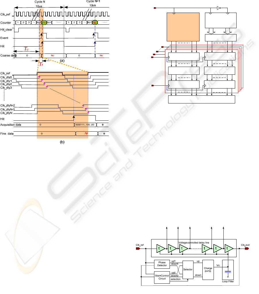
Figure 1 shows the operational principle of TDC
for small animal PET imaging system. The system is
reset with a cycle period of 10µs. The reset signal,
so called as Hit_clear in Figure 1, is the START
signal of TDC. A “Hit” signal generated by extern
pulse of an event is the STOP signal. The time
interval between the falling edge of Hit_clear and
the rising edge of Hit are measured by TDC chip. In
coarse conversion level, a counter is utilized to count
numbers. The counter commences to count at the
falling edge of Hit_clear and is interrupted while a
rising edge of “Hit” signal arrives. The last number
is read out as coarse data . In fine conversion step,
the delayed clock is generated by multiphase
generator. The state of the multiphase is readout by
rising edge of Hit signal. The acquisition data is then
converted to binary code. The total time can be
described as,
T
tdc
= N
c
× T
ref
+ N
f
× T
bin
(1)
Where, T
tdc
is the total time measured by TDC;
N
c
and N
f
are coarse and fine data, respectively; T
ref
and T
bin
are reference clock period and bin size of
TDC, respectively.
In the architecture based on two-level conversion
scheme, multiphase generators become the key part
of the whole design. As a solution, an array of DLLs
is proposed. An important advantage of array of
DLLs is that better resolution (less than 100ps) can
IMAGAPP 2009 - International Conference on Imaging Theory and Applications
172
easily obtained with either high frequency of
reference clock.
Figure 2 shows the architecture of array of DLLs
(ADLL) (Christiansen, 1996), (Mota and
Christiansen, 1998). Following the functions of
ADLL, 140-phase delayed clocks are generated by
the array.
Figure 1: Timing of TDC using two-level conversion
scheme for PET imaging system. (a) Timing of coarse
conversion. (b) Timing of fine conversion.
The states of phases are then read out as 140-bit
acquisition data when a HIT signal arrives. The
acquisition data is converted to 8-bit fine data by an
encoder. Double counter technique is proposed for
improving the reliability of 10-bit coarse data. We
propose gray counters instead of binary counters for
reducing the power dissipation. The array of DLLs
and counters are shared by N channels. Every
channel has its readout circuit with a signal of event.
A pipeline FIFO circuit is needed for buffering the
data coming from N channels. The last time words
are output in serial.
3 CIRCUIT DESCRIPTION
3.1 Low-jitter Delay-locked Loop
A full-analog DLL, shown in Figure 3, is selected
due to its high performance such as low jitter and
wide operational range. The DLL consists of
Voltage-controlled delay line, phase detector, charge
pump and loop filter. A start-control block is
embedded in the circuits to solve the false-lock
problem (Chang et al., 2002).
The blocks of DLLs are designed under the
consideration of low-jitter characteristic. A current-
Hit<N>
Array of Delay-
Locked Loops
(ADLL)
Double 10-bit
Gray Counter
(#1,#2)
Clk_ref
MUX21
X10 X10
Hit<1>
140-bit
Acqusition Registers
Thermometer-to-Binary
Converter
8-bit Readout Registers
10-bit
Acqusition Registers
Gray-to-Binary Converter
10-bit Readout Registers
Clk_read
Hit<2>
Hit<3>
Pipeline FIFO
Figure 2: The architecture of TDC based on an array of
DLLs (ADLL).
starved delay cell with DC current source is chosen
as our solution. A DC current source, realized by
MOS transistors (Mbp and Mbn in Figure 4 (a)), is
added to delay cell for reducing the slope of the
curve of delay time versus controlled voltage, shown
in Figure
4 (b). The mismatch in VCDL is an
intrinsic problem for DLL design. The unique way
to reduce mismatch is using match strategies in
layout design such as symmetric, interdigital and
common centroid.
A dynamic phase detector (Figure 5 (a)),
consisted of two True-single-phase clocking (TSPC)
flip-flop, is chosen due to its simple architecture and
other advantages such as high operational frequency
and no dead zone.
Clk_dly<0>
Clk_dly<1>
Clk_dly<2>
Clk_dly<n-2>
Clk_dly<n-1>
Figure 3: The architecture of a full-analog DLL. A start-
control circuit is added to detect the phase difference of
reference clock and output clock.
A 71PS-RESOLUTION MULTI-CHANNEL CMOS TIME-TO-DIGITAL CONVERTER FOR POSITRON EMISSION
TOMOGRAPHY IMAGING APPLICATIONS
173
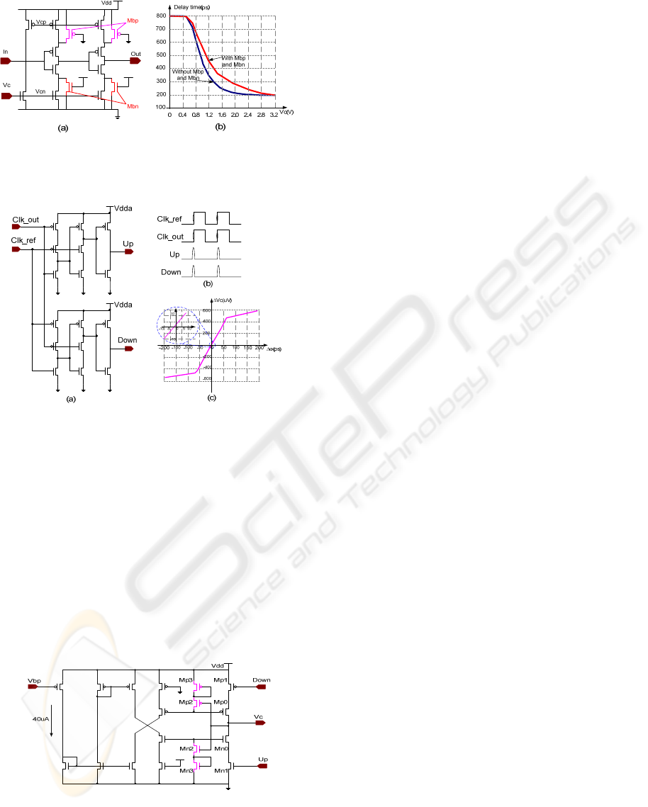
Figure 4: The design of delay cells. (a)Schematic of
current-starved delay cell; (b) the characteristic curve of
single delay cell.
Figure 5: Phase detector using TSPC flip-flop. (a)
Schematic; (b) timing when DLL is locked;(c)
Characteristic curve for phase detector.
Figure 6 shows the proposed charge pump
circuit. The charge pump is optimized by adding a
feedback circuit to improve the mismatch of charge
current and discharge current. The current mismatch
problem comes from channel length modulation of
Mp0 and Mn0 due to the output voltage (Vc) is
changed.
The loop filter is only a capacitor of 100pF. The
capacitor is implemented by MOS-capacitor in AMS
CMOS 0.35µm technology. Its die size is
90×570µm2.
Figure 6: Proposed charge pump circuit.
3.2 Array of DLLs (ADLL)
Two kinds of DLLs are employed for construction
of the array. The time taps of delay cells in both
classes of DLLs are T
m
and T
n
, respectively. The bin
size of ADLL can be obtained by delay difference of
T
m
and T
n
(where T
m
> T
n
). In order to generate time
taps, several functions in the following should be
satisfied (Christiansen, 1996), (Mota and
Christiansen, 1998).
T
bin
= T
m
− T
n
(2)
T
m
= T
clk
/ m (3)
T
n
= T
clk
/ n (4)
F = m / ( n − m ) (5)
where T
bin
is the bin size of ADLL, which is also
described as ∆t; T
clk
is period of reference clock; m
and n are the number of two kinds of DLLs
respectively; F is the number of DLL with n delay
cells.
In our design, m and n are chosen as 28 and 35
respectively; Then we have F=4 and T
clk
= 140∆t.
T
m
and T
n
are 5∆t and 4∆t respectively. T
clk
is
dependent on the characteristics of delay cells and
requirement of ∆t. The architecture of the array of
DLLs is shown in Figure 7. One DLL with delay
time of T
m
is DLL28, while Four DLLs with delay
time of T
n
are DLL35s (DLL35#0 to DLL35#3).
Four reference clocks of DLL35’s are generated by
DLL28
The ADLL consists of a low-jitter DLL with 28
delay cells (DLL28), four low-jitter DLL with 35
delay cells (DLL35), a current-to-voltage conversion
block (IVC) and a power-on reset unit (POR). The
architecture of ADLL is shown in Figure 7. The
low-jitter DLL’s described in section 3.1. The
unique difference of DLL28 and DLL35 is the
number of VCDL. An IVC is designed for reducing
the number of pads and the current mismatch of
charge pump in DLLs. The power-on reset unit is
employed for enhancing the sensitive of reset
function. The sequence of outputs in four DLL35s is
disorderly. A lookup table is needed to indicate the
relationship between outputs of DLL35s and outputs
of ADLL.
3.3 Data Readout Circuits
The Data Readout Circuits of one channel are
consisted of fine-data readout unit, coarse-data
readout unit and Hit generating circuit. The fine-data
readout unit is shown in Figure 8.
140-bit registers should be arranged in the first
position for reading out the state of 140 phases.
However, a duty cycle correction circuits should
be employed before the registers because the
delayed clocks generated by voltage controlled delay
IMAGAPP 2009 - International Conference on Imaging Theory and Applications
174
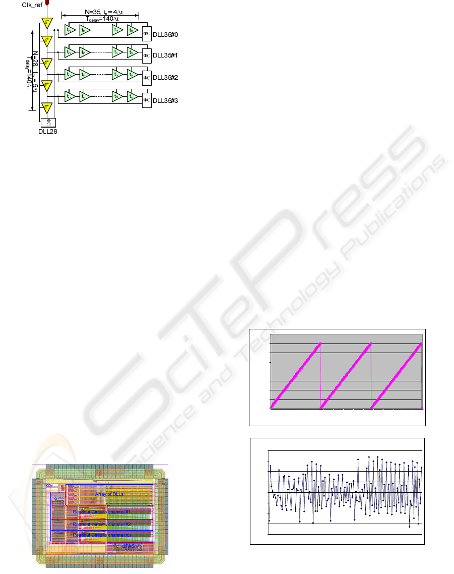
Figure 7: Topology of Array of DLL.
line (VCDL) have a duty cycle problem. Moreover,
the state of new phases is accurately readout and the
acquisition data are easily converted to binary code.
Hit signal is processed by this circuit to balance the
delay of signal caused by D flip-flop. A 140-bit
thermometer-to-binary converter is employed for 8-
bit fine data conversion. Another second-level 8-bit
registers are set after the conversion process. For
recording the coarse data, two-level registers are
embedded in the circuits reading out the number of
counter, balance the delay of signal. The data in all
the channels are readout serially in a cycle of 10µs.
4 PROTOTYPE CHIP AND
EXPERIMENTAL RESULTS
A prototype chip of TDC for PET imaging system is
designed in AMS 0.35µm CMOS IP4M technology.
In this evaluated chip, an array of low-jitter DLLs,
double 10-bit gray counters, 3-channel data readout
circuits, and a JTAG module are integrated. The
chip, which has 88 pads, occupies a die size of
8.4mm
2
. The layout is shown in Figure 8.
Figure 8: Layout of a prototype chip of TDC based on an
array of DLLs.
The performance of TDC is dependent on the
characteristics of DLLs in the array. The operational
range of DLLs is measured from 50MHz to
120MHz. The jitter performances at the last output
of the DLLs have been evaluated. The rms jitter is
less than 7ps and peak-to-peak jitter is less than
20ps. The total static power dissipation of each DLL
is about 4mW when the charge and discharge
current of charge pump is 40µA. The total power of
TDC is about 50mW while the total static power is
less than 10mW.
Figure 9(a) shows the post simulation result of
conversion curve of prototype chip in three clock
periods. The time taps is generated by random
emission algorithm. The differential nonlinearity
shown in Figure 9(b) is ±0.1LSB. The integral
nonlinearity is ±0.1LSB. The result is measured with
code density test by post simulation. The DNL of
last 10 data (from 129 to 139) is larger than others
due to the layout mismatch. It is indicated that the
proposed TDC has good performances on high
resolution, wide measure range, and low power
dissipation.
The overall performances of our prototype chip
are shown in Table 2. It is indicated that the TDC
using two-level conversion architecture based on
array of DLL can easily achieve smaller timing
resolution by using either a faster technology.
Moreover, wide dynamic range of measurement and
low power performances are obtained.
0
20
40
60
80
100
120
140
160
0, 05
1, 54
3, 03
4, 52
6, 01
7, 51
9
10,5
12
13,5
15
16,5
18
19,5
21,1
22,6
24,1
25,6
27,1
28,6
Time taps(ns)
digital output
(a)
-0,08
-0,06
-0,04
-0,02
0
0,02
0,04
0,06
0,08
1 7 13 19 25 31 37 43 49 55 61 67 73 79 85 91 97 103 109 115 121 127 133 139
Delay time error(LSB)
(b)
Figure 9: Experimental Results. (a) Conversion curve of
TDC in three clock period;(b) Differential nonlinearity of
TDC prototype chip.
A 71PS-RESOLUTION MULTI-CHANNEL CMOS TIME-TO-DIGITAL CONVERTER FOR POSITRON EMISSION
TOMOGRAPHY IMAGING APPLICATIONS
175
5 CONCLUSIONS
This paper describes the design of a high-resolution
multi-channel TDC applied for biomedical imaging
applications. A two-level scheme based on array of
DLLs has been successfully applied for TDC. A
prototype chip of 3-channel TDC for PET Imaging
systems is designed and fabricated in 0.35µm
CMOS IP4M technology. The bin size of TDC is
reduced to 71ps. From the analysis of results, the
array of DLLs has low-jitter performances and the
TDC has some advantages on high resolution, wide
measure range and low power.
For further development, the circuits will be
extended to 64-channel TDC for small animal PET
imaging systems. This kind of TDC can also be
widely used for particle life detection in high energy
physics and space applications. However, the array
of DLLs occupies large die size. Tradeoff between
bin size of TDC and die size should be considered
for different applications.
Table 1: Overall performances of the prototype chip.
[2] [3] [4] Our work
Architect
ure
ADC
Single
DLL
hierarchical
delay
Array of
DLLs
Process
CMOS
0.5µm
CMOS
0.35µm
CMOS
0.35µm
CMOS
0.35µm
LSB(min
.)
312.5p
s
244ps 312.5ps 71ps
Referenc
e Clock
- 32 MHz 500MHz 100 MHz
Dynamic
Range
80ns - 2ns 10µs
DNL
0.2LS
B
0.2 LSB 1.25LSB < 0.1LSB
INL
0.3LS
B
<1 % 1.45LSB <0.1LSB
Power
175m
W
14 mW 1mW 50mW
REFERENCES
Mbow, N.A, Bard, P., Brasse, D, et al. “A Full-Custom
Mixed-Signal CMOS Front-End Readout Chip for
High Efficiency Small Animal PET Imaging”, 14th
IEEE International Conference on Electronics,
Circuits and Systems, pp475-478, Dec. 2007.
Brian K. Swann, Benjamin J. Blalock, Lloyd G. Clonts, et
al. “A 100-ps Time-Resolution CMOS Time-to-
Digital Converter for Positron Emission Tomography
Imaging Applications” , IEEE Journal of Solid-State
Circuit, Vol. 39, pp. 1839-1852, NOV.2004.
O. Bourrion, L. Gallin-Martel. An integrated CMOS
Time-to-digital converter for coincidence detection in
a liquid Xenon PET prototype. nuclear instruments
and methods in physics research section A, Volume
563, Issue 1,pp 100-103, 2006.
A. S. Yousif and J.W. Haslett. “A fine resolution TDC
architecture for next generation PET imaging”, IEEE
Trans. Nucl. Sci, vol. 54, pp 1574 - 1582, October
2007.G.H. Li and H.P. Chou. “A high resolution
Time-to-digital Converter using two-level vernier
delay line technique”. Nuclear Science Symposium
Conference Record, 2007. NSS '07. IEEE, vol. 1, pp
276-280, Nov. 2007.
J. Christiansen. “An integrated high resolution CMOS
timing generator based on an array of Delay locked
loops”. IEEE journal of solid-state circuits.Vol.31, pp
952-957, July 1996
M. Mota, and J. Christiansen, “A Four Channel, Self-
Calibrating, High-Resolution Time-to-Digital
Converter,” Proc. IEEE Int’l Conf. Electronics,
Circuits, and Systems (ICECS’98), Vol. 2, pp. 155-
159, 1998.
H. Chang, J.Lin, and C. Yang, et al. “A wide-range delay-
locked loop with a fixed latency of one clock cycle”,
IEEE journal of solid-state circuits, vol.37, pp 1021-
1027. Aug. 2002.
IMAGAPP 2009 - International Conference on Imaging Theory and Applications
176
