
Nanoscale Education for Semiconductor Design
Walid Ibrahim and Yacine Atif
College of Information Technology, UAE University, Al Ain, U.A.E.
Keywords:
Nanotechnology, Learning Processes, Learning Objects, Curriculum Design, Nanofabrication, Bottom-up,
Top-down.
Abstract:
Over the last decades, nanotechnology had established itself as the upcoming revolution in science and tech-
nology. The ability of manipulating material at the atomic and molecular levels allowed nanotechnology to
open an entirely new paradigm of devices and products. In the semiconductor industry several new nanode-
vices have been proposed to replace the classical CMOS devices that have been used over the last four decades.
These new nanodevices have shown significant potential to overcome the fundamental limits of current CMOS
devices. However, limited educational resources and processes are available to prepare future nanotechnology
engineers and scientists to integrate these promising nanodevices into the main semiconductor manufacturing
streams. This paper proposes new learning structures and processes to propagate nanotechnology learning
resources over the pervasive Web. The proposed approach is illustrated by a case study centered around the
manufacturing of future nanodevices. We adopt standard structures and processes to organize and navigate
through digital instructional contents, such as IEEE LOM and IMS LD. In doing so, we aim at streamlining
the propagation of reusable repositories across the open Web to facilitate the integration of nanotechnology
learning resources into the rising social trend of massively open online courses (or MOOCs).
1 INTRODUCTION
Nanotechnology was formally defined in the 1999
NSF workshop report as “the ability to control and re-
structure the matter at the atomic and molecular levels
in the range of approximately 1–100 nm, and exploit-
ing the distinct properties and phenomena at that scale
as compared to those associated with single atoms or
molecules or bulk behavior. The aim is to create ma-
terials, devices, and systems with fundamentally new
properties and functions by engineering their small
structure” (Roco et al., 2000). In 2001 Uddin and
Chowdhury (Uddin and Chowdhury, 2001) stated that
the fundamental objective of nanotechnology is to
model, simulate, design and manufacture nanostruc-
tures and nanodevices with extraordinary properties
and assemble them economically into a working sys-
tem with revolutionary functional capabilities.
Applications in a wide spectrum of areas ranging
from nanomaterials to industry-specific applications
in biotechnology, electronics and energy, are creat-
ing unique opportunities all over the World. With
the latest advancement in nanolithography and opti-
cal proximity correction, the semiconductor industry
was successfully able to scale the transistor size fur-
ther to 20nm. This deep scaling into the nanometer
range has enabled several new mobile and commu-
nication applications including wearable computers,
intelligent handheld devices, healthcare implantable
devices , and self-powered wireless sensor networks
to mention a few. Today, there are more than 1,300
consumer products containing nanotechnology com-
ponents, while the inventory of products has grown
by over 500% in the last five years (Rodgers et al.,
2013). Trends suggest that by 2020 there will be a 3
trillion dollar market with 6 million employees in this
field (Roco, 2011).
In order to sustain this successful trend, it is essen-
tial to have sufficient workforce with an intensive and
focused training in nanotechnology. Unfortunately,
because of the interdisciplinary nature of the nan-
otechnology field (Porter and Youtie, 2009), this kind
of workforce is hard to develop. A skilled nanotech-
nology specialist should have good understanding of
several other science and engineering fields includ-
ing math, material and biomedical sciences, chem-
istry, physics, computer and environmental sciences,
among others. Currently, due to the lack of a proper
nanotechnology education, nanotechnology nspecial-
ists develop the required knowledge through training
courses and on the job learning experience.
Nanotechnology is rapidly growing as a separate
520
Ibrahim W. and Atif Y..
Nanoscale Education for Semiconductor Design.
DOI: 10.5220/0004956705200525
In Proceedings of the 6th International Conference on Computer Supported Education (CSEDU-2014), pages 520-525
ISBN: 978-989-758-020-8
Copyright
c
2014 SCITEPRESS (Science and Technology Publications, Lda.)

discipline by itself (McNally, 2013). However, one
major challenge asscoiated with the growth of this
discipline is the substantial cost required to provide
laboratory experiences. These hands-on practices are
essential to experience nanoscale matter (atoms and
molecules), and to design nanodevices and systems.
The associated cost can be reduced significantly by
relying on reusable electronic simulations and Web-
based repository of concept resources.
Another typical aspect in nanotechnology educa-
tion, which is not well supported in existing digital
instructional approaches, is the “zoom” effect, which
hierarchically and gradually reveals the infinitesimal
structures of nanomaterial. An alternative “assembly”
effect could empower existing digital instruction to
get learners exposed to both bottom-up and top-down
approaches of nanostructures manufacturing. In this
paper, we propose to augment existing learning tech-
nology standards for supportingthe design and the de-
velopment of virtual learning environments.
We adopt standard structures to organize digital
instructional contents and processes, such as IEEE
LOM (Atif et al., 2003) and IMS SCORM (Hsu et al.,
2010). In doing so, we aim at streamlining the prop-
agation of reusable repositories across the open Web
to facilitate the integration of nanotechnology learn-
ing resources into the rising social trend of Massively
Open Online Courses (or MOOCs) (Zhang, 2013).
2 BACKGROUND AND RELATED
WORKS
There are several challenges facing the integration of
nanotechnology into the mainstream of undergradu-
ate engineering curriculum. First, it is important to
increase the awareness of high school and the first
year engineering students about how the nanotech-
nology will shape our future. To this extend, Jones
et al. (Jones et al., 2003) investigated the feasibility
of allowing students in high school classrooms to con-
duct nanotechnology experiments through controlling
remotely scientific equipments over the Web. Stu-
dents had access to the nanoManipulator tool which
gave them the ability to control an atomic force mi-
croscope over the Internet. The authors believe that
most students were excited about the experience and
developed more accurate concepts regarding nanome-
ter scale as well as 2D and 3D virus morphology.
Another study funded by NSF focused on in-
creasing the nanotechnology awareness for both high
school and first year engineering students (Rodgers
et al., 2013)showed that student had difficulties
defining nanotechnology and its scale. This study
also highlighted computer graphics, visualized siz-
ing charts, and educational videos as effective tech-
niques for helping students understand nanotechnol-
ogy. Moreover,the study showed that connectingnan-
otechnology to various science and engineering fields
could serve as a catalyst method for introducing and
increasing students’ awareness and understanding of
nanotechnology scope.
To reduce the anticipated lab cost, (Sarangan et al.,
2013) suggested the use of a computer based nanofab
trainer. The proposed trainer would allow students
to practice real-life processes and tools as opposed to
normal simulators used for predicting physical phe-
nomena. They also proposed a multimedia system
to bring live interactive demonstrations from exist-
ing nanotechnology laboratories and cleanrooms to
the classrooms. Molecular Workbench software is an-
other tool proposed by Xie and Lee (Xie and Lee,
2012) for teaching nanotechnology concepts. The
tool provides a virtual laboratory in which simulated
nanoscale processes can be examined and manipu-
lated on a computer screen in real time. The au-
thors conducted a pilot study iwhich showed that
simulation-based experimentations can be success-
fully used for undergraduate students to develop an
integrated understanding of concepts in nanotechnol-
ogy at their own pace.
At the same time there are some efforts to incorpo-
rate nanotechnology into the mainstream of an under-
graduate engineering curriculum. Uddin and Chowd-
hury (Uddin and Chowdhury, 2001) proposed the con-
tent of three fundamental courses to be integrated into
an undergraduate engineering curriculum and sug-
gested that the concepts of nanotechnology should be
introduced during freshman and sophomore engineer-
ing courses. They also suggested modifying the out-
comes of junior and senior design courses to include
the modeling, simulation, control and optimization of
nanodevices and systems.
However, the common factor in the above instruc-
tional design approaches is the lack of a standard plat-
form for Web based education to create a space for
educators to share experiences and to reach a wide
community of learners.
Electronic learning production is multilayered as
shown in Figure 1. The core layer is the learning
object, which subsumes learning items following a
standard vocabulary defined by IEEE LOM specifi-
cation. Each item, in turn, points to a resource in
the resources layer. As illustrated in Figure 1, some
resources may reference files or contents outside the
packaged contents through a URL.
Learning objects metadata is a standard structure
to describe educational objects. The IEEE LOM stan-
NanoscaleEducationforSemiconductorDesign
521
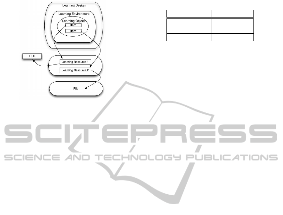
Figure 1: Learning Resource Layers.
dard specifies the vocabulary required to describe a
learning object, so it can be used, re-used or refer-
enced in technology supported learning. Learning ob-
jects typically incorporate contents to aid learners and
education-providers carry out their activities. This
content can be in a variety of electronic formats, in-
cluding (X)HTML, RTF, PDF, or simply a URL. A
learning object may be delivered within a specific en-
vironment such as a simulated laboratory application.
Finally, a learning design may dictate the navigation
through a sequence of learning objects. This process
obeys a standard specification labeled IMS-LD (IMS
Learning Design), which we will further present as
part of our proposed framework later in this paper.
A learning object structure includes typical cate-
gories following an XML-based specification of LOM
standard. This structure recognizes domain-specific
requirements, which include a set of functional and
non-functional capabilities that are deemed common
to learner-assistant software agents. A LOM struc-
ture consists of the following elements which we used
in our specifications: general, lifecycle,
Technical,
Educational, Rights, Relations
. We particu-
larly focus on extending the
Relation
attribute to
mimic advocated pedagogical processes in nanoscale
education.
3 LEARNING DESIGN FOR
NANOSCALE EDUCATION
Current LOM metadata information need to be re-
purposed to explicitly represent the specification of
nanoscale instructional units. This form of instruc-
tional units relies on semantic relationships between
learning resources to introduce learners to nanoma-
terials (Manning and Monetti, 2013). Semiconductor
design could involve bottom-up or top-downnanofab-
Table 1: Relationships in Nano-Learning Objects.
Relationship LOM element
Association Requires
Aggregation isBasedOn
Generalization hasPart
rication processes, using clusters of nanomaterial el-
ements. This approach to the pyramid of educa-
tion allows learners to advance through various disci-
plines that focus on phenomena and methods related
to length scales (Roco, 2003). The objective is to pro-
vide a progressively comprehensive nanoscale educa-
tion with connected and integrated knowledge to pro-
vide a holistic view, and a deductive understanding to
learners.
Learning resources in nanoscale education, are
structured as nano-learning objects, which describe
structural relationships of learning content in or-
der to support association and aggregation connec-
tions . These relationships could make use of
the
Relation->Kind
element of LOM attributes, as
shown in Table 1.
We define three types of relationships. The as-
sociation relationship guides learners to prerequisite
knowledge, whereas the aggregation relationship de-
fines “the degree to which a digital learning resource
is made up of other digital learning resources” (Na-
tional Science Foundation, 2004). Finally, the gener-
alization relationship refers to content assets or sub-
topics.
Collections of learning objects can be further or-
ganized and sequenced to form a learning compo-
nent, which refers to a lesson or a course. Sequencing
learning objects could be modeled through the use of
a learning design language, such as the IMS-LD (for
Learning Design), developed by IMS in 2003 (Koper
et al., 2003). The conceptual structure of learning de-
sign is based on a set of concepts or building blocks
that support the interaction among roles, activities and
environments. In the case of the IMS-LD, each per-
son may be assigned a role (either a learner or staff).
Based on the assigned role and the specified learn-
ing goal, each person performs an activity within a
specific environment. This could be for example a
particular experiment in a simulated laboratory envi-
ronment. The activity may involve both the learner
and a remote laboratorystaff. Our proposedhierarchi-
cal learning processes are based on IMS-LD standard,
which sequences learning objects using the aggrega-
tion or generalization links for bottom-up or top-down
learning designs. Each learning object may further be
explored through association links.
Teachers and instruction designers need a specifi-
cation of nanoscale education to express related learn-
CSEDU2014-6thInternationalConferenceonComputerSupportedEducation
522

ing activities. An IMS-LD compliant specification
lends itself to be used by existing graphical authoring
tools and engines to play the resulting specifications
(Griffiths et al., 2008; McAndrew et al., 2005). To fa-
cilitate nanoscale learning developments, we propose
ready-made templates that can be further refined to
create finished modules (called learning units). These
templates guide instructors and content providers to
build structured learning contents. We call these tem-
plates Nanoscale Learning Design Patterns (NLDPs).
They are analogous to Web page templates (e.g. avail-
able in Microsoft Front Page) to produce finished Web
pages as content and structure are separated. Figure 2
illustrates this IMS-LD based learning design pattern
for our nanoscale education model. NLDPs could be
implemented using an appropriate editor. The pro-
vision of a dedicated high-level nanoscale learning
editor supports teachers in the process of creating
nanoscale learning units by starting from existing pat-
terns.
The successive levels in the proposed learning de-
sign reflect the progressive bottom-up or top-down
content coverage. Each levels is supported by a set
of activities, which involve either learner or supervis-
ing staff. The environment entity indicates the exper-
imental setup to carry out those activities, such as a
simulated laboratory as discussed earlier in Figure 1.
4 SEMICONDUCTOR DESIGN
INSTRUCTION
College students should get first-hand experience on
how to fabricate various types of nanodevices and
how to use them to design functional nanosystems.
Therefore In additional to the classical CMOS pro-
cesses, the proposed cyber-infrastructure containers
should include learning objects with resources to in-
troduce learners to carbon nano tubes (CNTs) and
their unique properties such as their extraordinary
strength and thermal conductivity. This learning ob-
ject also includes resources to explore the electrical
properties of CNTs and their usage as field effect tran-
sistors (CNTFET). Another learning object embeds
motivational resources on the latest developments in
semiconductor nanowires and their vast applications
as logic devices, photo-detectors, biomedical sensors,
thermoelectric generators, and memory devices. Sub-
sequent (optional) learning objects could be used to
introduce students to other types of nanodevices such
as molecular resonant tunneling devices , single elec-
tron transistors , quantum-dot cellular automata de-
vices, or any other future nanodevicesas they become
more developed and practical. These learning objects
form the electronic repository of resources which is
structured following the framework presented in Fig-
ure 1.
The cognitive navigational process through learn-
ing objects and their underlying instructional environ-
ments follows the methods used to fabricate the above
mentioned nanodevices. These methods and hence
the proposed learning path could hierarchically fol-
low bottom-up or top-down approaches. Bottom-up
methods are those where the nanodevices are gradu-
ally assembled starting from the atom and the molec-
ular levels in an additive fashion until the desired de-
vice is built. On the other hand, the top-down meth-
ods start from a bulk substrate and use imaging and
etching processes to sculpt the device.
The top-down method relies on using several pho-
tolithography phases to engrave devices on a substrate
and connect them together to realize a specific circuit
design. Each photolithography phase usually con-
sists of several steps , which we put together using
“
hasPart
” attribute (see Table 1) of LOM’s relation
tag.
The photolithography process is very mature as
it has been successfully used by the semiconduc-
tor industry since 1970s. However the resolution
of the photolithography process is limited by the
wavelength of the light source used in the process.
Current photolithography process uses deep ultravi-
olet 193 nm laser and liquid immersion techniques
along with optical proximity correction to achieve
feature length less than 20nm. In order to use the
lithography method for future nanodevices, novel
processes are needed to reduce the resolution fur-
ther to few nanometers. Hence, in addition to the
classical photolithography, additional learning ob-
jects could include scanning, scanning probe, e-beam,
soft, nanoprint, nanosphere, and colloidal lithography
techniques.
As a result of the massive government and in-
dustry investments in nanofabrication research, sev-
eral bottom-up fabrication processes have matured
over the last decade. This suggests an alternative
navigation approach of learning objects with relation
tag value set to “
isBasedOn
” to aggregate compos-
ing learning objects together. These processes and
hence the induced instructional navigation can be di-
vided into chemical synthesis and self-assembly ones.
Self-assembly processes aggregate learning objects
about molecular self-assembly and DNA-scaffolding
processes. The chemical synthesis processes, on the
other hand, aggregate learning objects on gas-phase
and liquid-phase resources to manufacture nanopar-
ticles. The gas-phase subgroup may further aggre-
gate learning objects that illustrate the details of
NanoscaleEducationforSemiconductorDesign
523
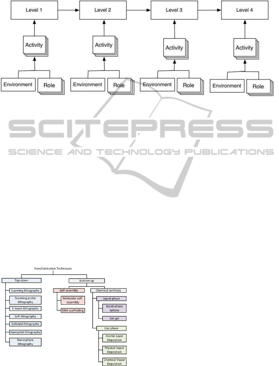
Figure 2: Nanoscale Learning Design.
atomic layer deposition , physical vapor deposition ,
and chemical vapor deposition processes. Similarly,
Sol–gel , and liquid-phase epitaxy learning objects
could be included under the liquid-phase subgroup.
It is obvious that the proposed learning objects
mentioned above are highly interdisciplinary. The ed-
ucational material covers a wide range of topics in-
cluding engineering, chemistry, physics, material sci-
ence, and biology in case of molecular self-assembly
and DNA-scaffolding. Having these learning ob-
jects correlated in a bottom-up and top-down ap-
proaches following the navigational structure shown
in Figure 2 organizes the contributions from instruc-
tors and scientists across multiple disciplines. The
open Web design structure offers also interaction op-
portunities and best practice sharing of instructional
scenarios among instructors Worldwide. Figure 3
shows the hierarchy of nanofabrication learning ob-
jects and their navigational sequence across the pro-
posed cyber-infrastructure design container discussed
earlier in Section 3.
Figure 3: Nanofabrication unites proposed for inclusion in
the cyber-infrastructure containers.
In addition to the top-down and bottom-up pro-
cesses, there are also few other processes such as
block copolymer lithography (Bates et al., 2013)that
combines the bottom-up self-assembly process with
top-down lithographic one, which calls for further
customization of the learning design structure shown
in Figure 2.
5 CONCLUSION
In view of the current shortage in nanotechnology ed-
ucational resources, we proposed standard Web-based
structures and processes for instructors to share edu-
cational material and for learners to personalize their
learning experience in nanotechnology. The novel
learning structure extends the current LOM metadata
to explicitly represent the specifications of nanoscale
instructional units based on expanding the standard
Relation
tag of LOM standard with three attributes:
Requires
,
isBasedOn
and
hasPart
. Following this
design structure, we also adopted standard learn-
ing processes based on IMS-LD information model,
that we specifically tailored to accommodate the pro-
cesses of navigating through nanotechnology instruc-
tional material. To illustrate our approaches, we pro-
posed a semiconductor design case study which we
mapped on the proposed learning structure and pro-
cesses to assist instructors sharing and reusing learn-
ing resources via the pervasive Web. The aim is to fa-
cilitate the integration of nanotechnology learning re-
sources into the rising social trend of massively open
online courses (or MOOCs) to benefit a larger com-
munity of learners and thus advancing the future of
nanoscale developments.
CSEDU2014-6thInternationalConferenceonComputerSupportedEducation
524

REFERENCES
Atif, Y., Benlamri, R., and Berri, J. (2003). Learning ob-
jects based framework for self-adaptive learning. Ed-
ucation and Information Technologies.
Bates, C. M., Maher, M. J., Janes, D. W., Ellison, C. J., and
Willson, C. G. (2013). Block copolymer lithography.
Macromolecules.
Griffiths, D., Beauvoir, P., and Sharples, P. (2008). Ad-
vances in Editors for IMS LD in the TENCompetence
Project. In Eighth IEEE International Conference
on Advanced Learning Technologies. IEEE Computer
Society.
Hsu, Y.-C., Liu, Y.-C., and Chang, S.-S. (2010). A study
of SCORM-based Sharable Content Repository Man-
agement System. Information Management and En-
gineering (ICIME), 2010 The 2nd IEEE International
Conference on, pages 110–114.
Jones, M. G., Andre, T., Superfine, R., and Taylor, R.
(2003). Learning at the nanoscale: The impact of
students’ use of remote microscopy on concepts of
viruses, scale, and microscopy. Journal of Research
in Science Teaching, 40(3):303–322.
Koper, R., Olivier, B., and Anderson, T. (2003). IMS
Learning Design Information Model. IMS Global
Learning Consortium, Inc. [Online] available at:
http://www.imsglobal.org/learningdesign/ldv1p0/imsld
infov1p0.html.
Manning, T. J.and Monetti, D.M. (2013). Nano and Molec-
ular Cryptology: Hiding Information in Molecules
and Nanostructures. Journal of Nano Education,
5(2):93–108.
McAndrew, P., Nadolski, R., and Little, A. (2005). De-
veloping an approach for Learning Design Players.
Special Issue: Advances in Learning Design of Jour-
nal of Interactive Media in Education, available at
http://www-jime.open.ac.uk/article/2005-14/287, ac-
cessed on June 19, 2012), 1.
McNally, H. A. (2013). Maximizing nanotechnology ed-
ucation at purdue university: Its integration into the
electrical engineering technology curriculum. Nan-
otechnology Magazine, IEEE, 7(3):19–22.
National Science Foundation (2004). The
reusable learning website. Available at
http://www.reusablelearning.org/.
Porter, A. L. and Youtie, J. (2009). How interdisciplinary
is nanotechnology? Journal of Nanoparticle Re-
search, 11(5):1023–1041. PMID: 21170124 PMCID:
PMC2988207.
Roco, M. (2011). The long view of nanotechnology de-
velopment: The national nanotechnology initiative at
10 years. In Nanotechnology Research Directions for
Societal Needs in 2020, volume 1 of Science Policy
Reports, pages 1–28. Springer Netherlands.
Roco, M. C. (2003). Converging science and technology at
the nanoscale: opportunities for education and train-
ing. Nature Biotechnology, 21(10):1247–1249.
Roco, M. C., Williams, R. S., and Alivisatos, P. (2000).
Nanotechnology Research Directions: IWGN Work-
shop Report: Vision for Nanotechnology in the Next
Decade. Springer.
Rodgers, K. J., Diefes-Dux, H. A., and Madhavan, K.
(2013). First-year engineering students explore nan-
otechnology in engineering. In 41st European Society
for Rngineering Education (SEFI) Conference.
Sarangan, A., Haus, J. W., Jain, S. M., Moradmand, J., and
Reeder, N. (2013). Collaborative classroom tools for
nanotechnology process education. In 120th ASEE
Annual Conference and Exposition, pages Paper ID
–7689.
Uddin, M. and Chowdhury, A. R. (2001). Integration
of nanotechnology into the undergraduate engineer-
ing curriculum. In Proceedings of the International
Conference on Engineering Education, number 8B2,
pages 6–9.
Xie, C. and Lee, H.-S. (2012). A visual approach to nan-
otechnology education. The International Journal of
Engineering Education, 28(5):1006–1018.
Zhang, Y. (2013). Benefiting from MOOC. World Con-
ference on Educational Multimedia, 2013(1):1372–
1377.
NanoscaleEducationforSemiconductorDesign
525
