
A 6GS/S 8-Bit Current Steering DAC with Optimized Current Switch
Drive
Wenyuan Li, Juan Zhang and Chuyang Sun
Institute of RF-&OE-ICs, Southeast University, Nanjing 210096, China
Keywords: Digital-to-Analog Converter (DAC), CMOS, Very High-Speed, Current-steering.
Abstract: A 6GS/s 8-bit current-steering DAC in 0.13μm CMOS technology is presented. The 5-31 binary to
thermometer decoder and the switch drive signal are optimized, leading to obvious improvements in
dynamic performance. A minimum spurious free dynamic range (SFDR) of 34 dB has been achieved over
the full Nyquist bandwidth at 6GS/s. Total system power consumption is 95.44mW at 6GS/s with 2.98GHz
input signal. Core area of DAC occupies 0.13mm
2
without pads.
1 INTRODUCTION
Advancement in applications in the area of video and
ultra-wide-band (UWB) wireless communications
needs high-speed and low- to moderate-resolution
data converters so that the demand of DAC’s with
sampling frequency up to multi-GS/s has drastically
increased. In wide-band systems, analog
reconstruction filters with high performance always
increase complexity and power cost (Zhou et al.,
2003). To relax the stop-band slope requirement, it is
necessary to choose a reasonable structure for DAC’s
working at sampling data in the order of Gigahertz.
The push towards Gigahertz frequencies has
increased the demand for UWB DACs with maximal
SFDR. At Gigahertz frequencies, the switch
conversion time consumes a significant portion of the
clock period, degrading SFDR. Thus, in order to
improve dynamic performance, we proposes a novel
switch driver. In addition, complex direct
thermometer decoder will make drive and
synchronizing requirements more difficult to meet,
one method to solve the problems is to propose
distributed-row-decoders topology. Moreover, design
of high speed DAC’s are proven difficult (Bastos et
al., 1999; Bavel et al., 1998; Bosch et al., 1998),
tackling with process and parasitic problems.
In this paper, a digital-to-analog converter with
clock frequency up to 6GHz is presented. In section
II, the architecture of the current-steering DAC will
be discussed. In section III, some improvements to
optimize the 5-31 decoder and drive signal for
current switches and will be introduced along with
other building blocks. The simulation results will be
shown in section IV, and the conclusion will be given
in section V including contrast with other works.
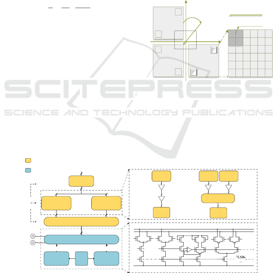
2 ARCHITECTURE
Current-steering DAC’s simply switch output unit
current from one terminal to the other according to
the drive signal, spending no time on charging scaled
capacitors so they are fast and can reduce the cost
considerably. Figure 1 shows the main structure used
in the implemented DAC. In order to compromise
between complexities versus static linearity, 5+3
segmentation has been applied. The most significant
5 bits (MSBs) are thermometer decoded generating
31-bit unary code to control MSB logic current cells.
Each one of logic cells has 4 physical current sources
connected in parallel. The least significant 3 bits
(LSBs) are also thermometer decoded, causing the
same delay with MSB decoding and minimizing the
output glitch. Each LSB physical current source is
equally divided into two LSB logical sources. And
the common gate MESFETs of LSB physical current
sources are biased by an error amplifier. The analog
block is powered separately from the digital block for
the reduction of noise coupling.
Li, W., Zhang, J. and Sun, C.
A 6GS/S 8-Bit Current Steering DAC with Optimized Current Switch Drive.
DOI: 10.5220/0006413100710075
In Proceedings of the 7th International Joint Conference on Pervasive and Embedded Computing and Communication Systems (PECCS 2017), pages 71-75
ISBN: 978-989-758-266-0
Copyright © 2017 by SCITEPRESS – Science and Technology Publications, Lda. All rights reserved
71
3 CIRCUIT IMPLEMENTATION
3.1 Current Cells Design
Current source array occupies the most area of
analog block because of restrain of static mismatch.
Assume two variables, A
β
and A
th
, as parameters of
static current mismatch variance. Reference
(Lakshmikumar et al., 1986) indicates that the
mismatch parameters, A
β
and A
th
, are inversely
proportional to the size of scaled current sources.
The relationship between current mismatch and
transistor size is presented more quantitatively in the
formula:
2
2
β
th
ov
4
A
A
I
I
WL WLV
,
where σ(I) is the standard deviation of current
mismatch and assigned 0.005 for the integral
nonlinearity (INL)-yield up to 99.7%
(Lakshmikumar et al., 1986). WL and V
ov
represents
transistor size and overdrive voltage respectively.
Reference (Schofield et al., 2001) introduces an
ingenious way to reduce graded and symmetrical
errors within the cell array in layout design. The
31*4 MSB unary sources are assigned in 4
concentric symmetrical cubes. Each cube has 6*6
numbered cells and cells share the same order
number over 4 cubes are connected in parallel. To
minimize the glitch, 7 LSB unary sources are
assigned in the center of the array (Figure 2).
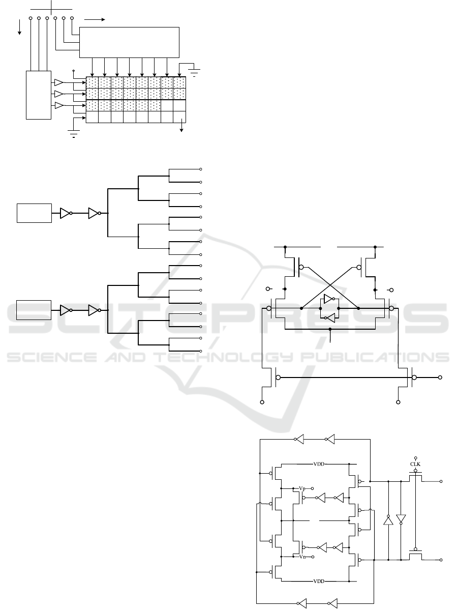
3.2 5-3 Thermometer Decoder and
Optimization
Since the circuit has to support up to the sampling
rate of 6GHz, driving and timing constraint is
imposed on the digital blocks. Complex direct
thermometer decoder of the 5 MSBs will make drive
and synchronizing requirements more difficult to
meet, so it is necessary to divide the decoder into
two stages. As shown in Figure 3, the first stage
consists of a 3-bit thermometer decoder and a 2-bit
thermometer decoder. The second stage is a routing
matrix which generates the final thermometer codes.
Each row decoder output drives 16 routing
matrix units and 4-order tree line. The delay of the
whole decoder is restrained less than one clock
period, so the size of driver
chain between row
decoder and routing matrix units is limited.
A
B
A
B A
B
2 4 13 36
20 22 31 18
32 25 7 3 21 23
14 16 34 30 12 5
28 6 15 17 26 19
1 24 33 35 8 10
27 29
9 11
Mirror image and shift
LSBs
LSBs Block
Figure 2: Current cells assignment.
And the connection of row decoder and the
matrix is very complex. One method to solve the
problems is to adopt distributed-row-decoders
topology (Figure 4). With the usage of reductant
decoder, the drive burden and line density are
effectively reduced. As a result, the decoder outputs
are robust and the DAC performance is promoted.
Input Latches
LSB
Thermometer
Decoder
MSB
Thermometer
Decoder
Improved Switch Driver
Switch Array
Unary LSB
Current Cell
Unary MSB
Current Cell
Bias
Digital Block
Analog Block
5b
3b
7b
31b
31b7b
Clock Distribution
OUT
38b
Logical Selection
Array
3-7 Decoder 2-3 Decoder
Retime
3-7 Decoder
Retime
31MSBs
...
31b
7b
LSBs
Decoder
MSBs
Decoder
Data
Inputs
OUT/
VDD
Figure 1: Main block of the DAC.
SPCS 2017 - International Conference on Signal Processing and Communication Systems
72
Q
5
Q
4
Q
3
1 1 0 1 0
(decimal base:22)
Column decoder
V
DD
Column 3-7 decoder
Row 2-3 decoder
1 1 1 1 1 1 0
1
1
0
22 high-level outputs
Q
7
Q
6
L
0
L
1
L
2
L
3
L
4
L
5
L
6
H
0
H
1
H
2
32
b
its routing matrix
Row decoder
Figure 3: 5 Bits binary to thermometer decoder.
Row decoder
Reductant
Row decoder
Figure 4: Distributed-row-decoder topology.
3.3 Optimizing the Current Switch
Diver
The massive size of the current cell leading to large
parasitic capacitor at the source of differential
switches makes it necessary to minimize the voltage
glitch at the source, because strong glitch will
drastically degenerate both static and dynamic index
of output signals. One effective solution is to
generate low-swing and high cross point differential
drive waveform, such that the voltage vibration at
the source will be diminished. Common drive circuit
is depicted in Figure 5(a). Vp and Vn are the drive
signals for switches, and they swing between VDD
and the reference low level, Vref. By enlarging the
size of M1, M4 and reducing the size of M2, M3, the
optimal cross point of differential output waveform
is attained, and the DAC linearity is maximized.
Figure 6 shows the simulation result. However, the
falling edge turns out to be too gentle while meeting
swing and trip point requirements. Figure 5(b)
shows the upgraded circuit. Transistors M5-8 copies
the same on-off operation from M1-4. In invertors I1
and I3 the size of P-FETs is much larger than that of
N-FETs. On the contrary, in invertor I2 and I4, the
size of N-FETs is much larger than that of N-FETs.
As the results, V3 and V4 are asymmetric pulses,
and the low-level period is shorter than that of the
high-level. When low level comes at V3 or V4, M9
or M10 will be opened accordingly, and the low
level period should not last too long, in case that M9
and M10 are still open as the signals at V3 and V4
rise. By properly sizing invertors I5-8, the delay
between the falling edge at Vn, Vp and turn-on
window of M9, M10 can be adjusted and as a result,
falling edge of driving signals will be optimized.
Figure 6 shows the contrast of two drive signals. The
upper signal is without optimization, and the lower
signal is with optimization. The glitch is diminished
and the low level step is clearer in the result with
optimization.
VDD
Vp
Vn
V1
V2
M1
M2 M3
M4
DATA
DATA/
CLK
Vref
Figure 5(a): Common switch driver.
Vref
M1
M2
M3
M4
M5
M6
M7
M8
M9
M10
V3
V4
I1I2
I4 I3
I5 I6
I7 I8
DATA/
DATA
Figure 5(b): Upgraded switch driver.
A 6GS/S 8-Bit Current Steering DAC with Optimized Current Switch Drive
73
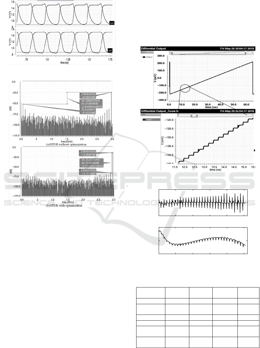
Figure 6: Contrast of drive waveforms.
Figure 7: Comparison of dynamic performance.
3.4 Comparison of Dynamic
Performance of DAC with and
without Optimization
Figure 7 shows the comparison of dynamic
performance of DAC with and without optimization.
The clock rate is 6GSPs and input signal bandwidth
is 2.96GHz. Apparently, the SFDR result with
optimization is 34dB better than without
optimization.
4 POST SIMULATION RESULTS
Figure 8 presents the step waveform when the input
code increases from 00000000 to 11111111 with the
code rate up to 4Gb/s. Associated differential
nonlinearity (DNL) along with INL are calculated
and results are shown in Figure 9. It is obvious that
switching glitch is restrained about 1 LSB and static
requirement is satisfied with both DNL and INL less
than 0.5 LSB (Figure 9). Dynamic performance is
simulated with different clock rate and different
inputs (Figure 10). At 4GSPs clock rate, with the
1.98GHz output signal bandwidth, SFDR is 53dB.
At 6GSPs clock rate, with the 2.96GHz output signal
bandwidth, SFDR is 33dB.
Figure 8: Step waveform of differential output.
Figure 9: Results of DNL and INL.
Table 1: Comparison with other works.
This work
(Zhao et
al., 2011)
(Li et al.,
2014)
(Xiong et
al., 2014)
Resolution 8 bits 14 bits 8
b
its 6 bits
Sampling
rate
6GS/s 2GS/s 2GS/s 8GS/s
DNL(LSB) 0.2 0.3 0.12 0.04
INL(LSB) 0.4 0.5 0.23 0.04
SFDR(dB)
33@
2.96GHz
70.2@
994MHz
49@
992MHz
34@
2.7GHz
Process
130nm
CMOS
65nm
CMOS
180nm
CMOS
65 nm
CMOS
0 50 100 150 200 250
-0.5
0
0.5
Code
INL
0 50 100 150 200 250
-0.2
0
0.2
Code
DNL
SPCS 2017 - International Conference on Signal Processing and Communication Systems
74
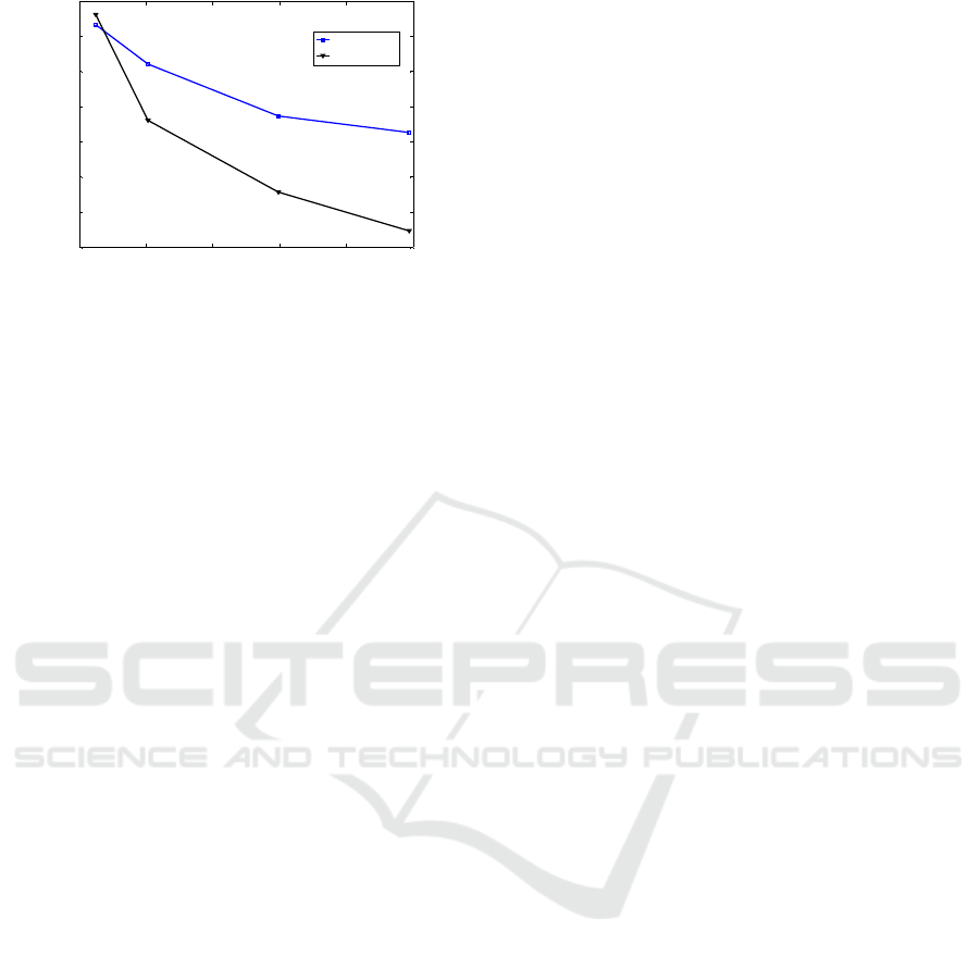
Figure 10: SFDR results of 8-bit DAC.
5 CONCLUSION
This paper has presented a 6GS/s 8bit DAC in
0.13μm CMOS technology. By properly sizing and
arranging the current source array, good statistic
performance has been achieved. By optimizing the
decoder and switch driver, the DAC can work at
6GSPs. The full scale output current of the DAC is
3.825mA and the power consumption is 95.44mW at
6G sampling rate with 2.96GHz input signal
bandwidth. Table I summarizes the DAC
performance and compares it with other recently
published very high-speed DACs. It can be learned
from the Table that the proposed DAC is able to
work at higher sampling rate. With the optimized
current switch, the proposed DAC achieves > 33dB
SFDR up to 2.96GHz where the signal frequency of
other reported DACs are limited to 2.7GHz.
ACKNOWLEDGEMENTS
We are sincerely thankful for the support from the
Project Funded by the Priority Academic Program
Development of Jiangsu Higher Education
Institutions (PAPD, No.1104007003), Natural
Science Foundation of China (No.61471119) and
Topnotch Academic Programs Project of Jiangsu
Higher Education Institutions (TAPP)
PPZY2015A035.
REFERENCES
Y. Zhou and J. Yuan, 2003. An 8-bit 100-MHz CMOS
Linear Interpolation DAC, IEEE Journal of
Solid-State Circuits, 38(10), pp. 1758-1761. doi:
10.1109/JSSC.2003.817593.
J. Bastos, A. M. Marques, M. S. J. Steyaert, and W.
Sansen, 1999. A 12-bit Intrinsic Accuracy High-speed
CMOS DAC, IEEE Journal of Solid-State Circuits,
33(12), pp. 1959-1969. DOI: 10.1109/4.735536.
N. van Bavel, 1998. A 325 MHz 3.3 V 10-bit CMOS D/A
Converter Core with Novel Latching Driver Circuit,
Custom Integrated Circuits Conference Proceedings
of the IEEE, Santa Clara, California, pp. 245-248.
DOI: 10.1109/CICC.1998.694973.
A. Van Den Bosch, M. Borremans, J. Vandenbussche, and
G. Van der Plas, 1998. A 12 bit 200 MHz Low Glitch
CMOS D/A Converter, Custom Integrated Circuits
Conference Proceedings of the IEEE, Santa Clara,
California, pp. 249-252. DOI: 10.1109/CICC.
1998.694974.
K. R. Lakshmikumar, R. A. Hadaway and M. A.
Copeland, 1986. Characterization and modeling of
mismatch in MOS transistors for precision analog
design, IEEE Journal of Solid-State Circuits, 21(6),
pp. 1057-1066. DOI: 10.1109/JSSC.1986.1052648.
W. G. J. Schofield and I. J. Dedic, 2001. Cell array
circuitry, U.S. Patent No. 6,236, 346. 22 May.
R. Li, Q. Zhao, T. Yi, and Z. Hong, 2011. A 14-bit 2-GS/s
DAC with SFDR>70dB up to 1-GHz in 65-nm
CMOS, IEEE 9th International Conference on ASIC,
Xiamen, China, pp. 500-503. doi:
10.1109/ASICON.2011.6157231.
W. Y. Li and T. X. Jiang, 2014. A 4-bit 5 GS/s Current
Steering DAC Integrated Circuit, Applied Mechanics
& Materials, 513-517, pp. 4555-4558.
DOI:10.4028/www.scientific.net/AMM.513-517.4555
W. Xiong, L. Wenyuan and S. Chuyang, 2014. An 8GS/s
6-bit current steering DAC in 65nm CMOS
technology, 2014 International Conference on
Advanced Technologies for Communications (ATC),
Hanoi, Vietnam, pp. 491-493. DOI:
10.1109/ATC.2014.7043438.
0 0.1 0.2 0.3 0.4 0.5
30
35
40
45
50
55
60
65
Fsig/Fclk
SFDR(dB)
Fclk=4GHz
Fclk=6GHz
A 6GS/S 8-Bit Current Steering DAC with Optimized Current Switch Drive
75
