
25Gbps Automotive Ethernet ECU PCB:
MDI Design Implementation and Insertion Loss Characterization
Jamila J. Borda
1
, Kirsten Matheus
1
and Friedel Gerfers
2
1
Department of Communications Network Technologies, BMW Group, Munich, Germany
2
Department of Computer Engineering and Microelectronics: Mixed Signal Circuit Design,
Technische Universitaet (TU) Berlin, Berlin, Germany
Keywords: Automotive Multi-Gigabit Ethernet, MultiGBASE-T1, 2.5GBASE-T1, 5GBASE-T1, 10GBASE-T1,
25GBASE-T1, ECU, PCB, MDI, Insertion Loss, Signal Attenuation.
Abstract: Physical Layer (PHY) Signal Integrity (SI) aspects of an Automotive Ethernet communication channel are
characterized using Radio Frequency (RF) parameters. With increasing Automotive Ethernet data rates,
communication channel signal attenuations (i.e., Insertion Loss (IL)) are significantly worsened. At 25Gbps
data rate, the communication in cars faces various electrical limits and all components (i.e., segments) of the
communication channel have to be optimized in order to reach the expected performance requirements. One
such component is the Electronic Control Unit (ECU) Printed Circuit Board (PCB) Media Independent
Interface (MDI). Consequently, for such high-speed links, ECU PCB electrical and material properties have
an impact on the overall IL. Considering the stringent Automotive Ethernet channel electrical requirements,
this study proposes and characterizes ECU PCB MDI design concepts for a 25Gbps in-vehicle Ethernet
connectivity. Furthermore, the design concepts are manufactured on test boards to characterize the
corresponding MDI signal IL budget. The characterizations are conducted using RF test bench measurement
and a defined simulation approach. Lastly, in relation to test bench measurements, this study investigates and
characterizes to what extent simulations can serve as either an alternative or a coexisting option for in-vehicle
25Gbps MDI IL characterizations, validations, and qualifications.
1 INTRODUCTION
Increasing in-vehicle communication channel
operating frequencies are accompanied with
increasing in-vehicle system sensitivity to
ElectroMagnetic Interference (EMI) and
channel/components signal ILs. This results from
steeper signal rise/fall SI timing requirements and
higher Nyquist frequencies (i.e., signal bandwidth) of
the ever-increasing data rates (Borda J. , 2022).
Consequently, essential PHY system performance
aspects of an Ethernet communication channel,
namely system design and implementation, are
impacted by these effects (Borda J. , 2022).
As a channel segment, the PCB MDI has a
meaningful contribution to the overall channel
performance in relation to SI and ElectroMagnetic
Compatibility (EMC) characteristics. Right after the
cable (i.e., link segment) IL, the PCB MDI serves as
the second largest contributing factor to the overall
channel IL. Link segment characterization for
25Gbps is referenced to the study in (Borda J. J.,
2022). Hence, the channel PHY system design and
implementation have to have a subsequent focus on
the ECU PCB. The MDI network comprises of passive
(and application dependent active) components. For
MultiGBASE-T1 data rates (2.5GBASE-T1/2.5Gbps,
5GBASE-T1/5Gbps, 10GBASE-T1/10Gbps, 25GBASE-
T1/25Gbps), the MDI network is reduced to Alternating
Current (AC) coupling capacitors (for blocking
undesired direct current) and Electrostatic Discharge
(ESD) protection device on each of the differential
traces (IEEE 802.3ch, 2020) (IEEE 802.3cy
(Unpublished), 2022). Figure 1 provides an overview
of the electrical Automotive Ethernet communication
channel with the defined MDI segment and several
other components (i.e., within this study
interchangeably also described as “segments”). For a
copper-based/electrical transmission, a Single
Communication Channel (SCC) extends through the
ECU PCB MDI up to the PHY transceiver (typically
having a Ball Grid Array (BGA) design type) MDI
74
Borda, J., Matheus, K. and Gerfers, F.
25Gbps Automotive Ethernet ECU PCB: MDI Design Implementation and Insertion Loss Characterization.
DOI: 10.5220/0011756000003479
In Proceedings of the 9th International Conference on Vehicle Technology and Intelligent Transport Systems (VEHITS 2023), pages 74-84
ISBN: 978-989-758-652-1; ISSN: 2184-495X
Copyright
c
2023 by SCITEPRESS – Science and Technology Publications, Lda. Under CC license (CC BY-NC-ND 4.0)

differential pair pads/pins (IEEE 802.3ch, 2020). The
MDI header connector can also be based on a multi-
port system. This is either because more than a single
differential pair port of the same interface is available,
or because “hybrid” multi-port connectors with a
blend of various communication interfaces (single
or/and differential based signals) as well as power
lines are being used (OPEN Alliance, 2020) (OPEN
Alliance, 2022).
Figure 1: Electrical Automotive Ethernet SCC showing the
MDI within the ECUs (Borda J. , 2022).
Several PCB electrical and material design
properties must be well defined and characterized to
ensure an optimum ECU PCB MDI signal IL budget
and subsequently SI retention for a 25Gbps
Automotive Ethernet channel:
(1) This starts off with having a proper selection
of dielectric materials to be used for the
complete ECU PCB design to accommodate
both the high-speed design and Automotive
requirements. One of its electrical properties
i.e., loss tangent (also known as dissipation
factor) plays a significant contribution to the
PCB MDI signal IL.
(2) Another contributing factor to the PCB MDI
signal IL is the design concept used for the
MDI differential pair trace layout.
Primarily, one differentiates between
microstrip (including embedded) and
Stripline PCB trace designs (Mittal, 2021).
ECU PCBs are typically densely populated
with several passive and active components
occupying the MDI segment. A trace layout
design structure targeting an optimum signal
IL budget must therefore be tailored to
ensure SI compliance.
(3) The overall PCB layer stackup concept
serves as an additional characteristic aspect
contributing to PCB MDI signal IL. To reach
an optimum PCB MDI IL, several layer
stackup design concepts must be thoroughly
thought out. Considering Automotive
channel requirements, these primarily
include, (1) how to define the layer stackup
(including signal and power planes, layer
counts), (2) defining optimum differential
pair trace lengths, width and spacing, and (3)
design concepts for current return paths and
the proper usage of vias to ensure
compliance to SI.
To the authors’ best knowledge, the
aforementioned ECU PCB design aspects are yet to
be thoroughly investigated and characterized in the
Automotive industry for 25Gbps electrical
Automotive Ethernet connectivity. This therefore
calls for having these aspects adapted and, in some
cases, the associated requirements and specifications
in regard to PHY ECU PCB MDI system design and
implementation need to be newly defined.
Furthermore, this study serves as an essential baseline
for the PHY system design technical feasibility study
for the deployment of 25Gbps Automotive Ethernet.
Initial investigations of this study focus on
defining optimum PCB MDI design concepts for
25Gbps data rate. Here, multiple PCB variants are
defined considering several electrical properties. To
emulate an ECU PCB, the design concepts are then
implemented to be used as Device Under Test (DUT)
for MDI IL characterization. Subsequent chapters
target the actual characterization of the PCB MDI IL.
Section 5 of this study discusses and defines the
technical feasibility of deploying ECU PCB MDI
simulations in correlation with a conventional test
bench measurement approach.
2 THEORETICAL BACKGROUND
Figure 2 shows the side-view of the MDI within the
ECU PCB defining the region on which the PCB MDI
RF characterization takes place.
Figure 2: Overview of the MDI within the ECU PCB.
Validation and characterization of ECU PCB
MDI design implementation primarily focuses on two
system performance parametric categories, namely SI
retention and compliance to EMC. The associated
electrical properties cover RF, transient, and channel
transmission line characteristic parameters (Borda J.
J., 2022) (OPEN Alliance, 2022) (OPEN Alliance,
2020). For SI, IL is the primary essential parameter
used to characterize the ECU PCB MDI in relation to
the Automotive Ethernet communication overall
25Gbps Automotive Ethernet ECU PCB: MDI Design Implementation and Insertion Loss Characterization
75

channel requirements (IEEE 802.3ch, 2020) (IEEE
802.3cy (Unpublished), 2022). Signal differential
pair trace characteristic impedance, propagation
delay, and an EMC-compliant PCB design are
typically additionally characterized at the PCB-level
independent of the communication channel. These
particular characterizations are however not further
covered within the scope of this study.
2.1 ECU PCB Total Losses
Generally, the overall ECU PCB total loss (i.e., IL)
𝛼
is a sum of dielectric losses 𝛼
, signal conductor
losses 𝛼
, leakage 𝛼
and radiation losses 𝛼
as
described in Equation (1 (Borda J. J., 2022) (Polar
Instruments, 2022) (Coonrod , 2013).
𝛼
𝛼
𝛼
𝛼
𝛼
(1)
Dielectric Losses: Dielectric losses are
associated with the dissipation factor 𝐷
(i.e., loss
tangent). The governing equation for this is described
and referenced in (Borda J. J., 2022) and (Mittal,
2021). Dielectric losses increase with operating
frequency due to changing ElectroMagnetic fields.
These changes cause the dielectric molecules to
vibrate faster and hence leading to more energy loss.
For high-speed transmission, lower loss tangents
favour lower energy losses in the dielectric material
(Knack, 2020).
Signal Conductor Losses: Conductor losses are
associated with numerous variables. Amongst these are
losses due to Skin-effect. At higher frequencies, i.e., in
the GHz range, the signal current flows predominately
on the conductor surface and the current density decays
exponentially towards the center of the conductor,
which causes the signal attenuation (Borda J. J., 2022)
(Polar Instruments, 2022) (Coonrod , 2013). Surface
roughness of a conductor is another issue contributing
to PCB conductor losses. This happens when a signal
conductor surface is rough causing longer wave
propagation paths and consequently creating more
losses. The losses are linked to parasitic inductances
from surface inductance of the current following in
partial loops in the copper metal profile (Coonrod ,
2013).
Leakage Losses: Leakage losses are usually in
relation to semiconductor grade materials. With the
materials used in PCB technology generally having
very high-volume resistance, leakage losses have an
almost negligible contribution to the total PCB losses
(Coonrod , 2013).
Radiation Losses: The occurrence of radiation
losses is design dependent. Energy lost from a PCB
circuit or from a transmission line radiated off to the
surrounding environment typically describes
radiation losses. These losses are at their maximum in
impedance transitions and signal transmitting areas of
the PCB. Radiation losses depend on the operating
frequency, the dielectric constant, and the PCB
substrate thickness (Coonrod , 2013).
Characterization of IL is conducted using Mixed-
Mode S-Parameter analysis. A description of these S-
Parameters is not covered within the scope of this
study. However, these are referenced to descriptions
found in (Borda J. J., 2022) and (Fan, Lu, Wai, &
Lok, 2003).
2.2 ECU PCB MDI Insertion Loss
For 25GBASE-T1, the PCB MDI IL is specified
based on maximum and minimum MDI differential
pair trace lengths. These trace lengths are 76.2mm
and 25.4mm respectively (IEEE 802.3ch, 2020)
(IEEE 802.3cy (Unpublished), 2022). The governing
equations for the maximum PCB MDI IL,
𝐼𝐿
,
and minimum IL 𝐼𝐿
,
are
described in Equation (2) and Equation (3)
respectively (IEEE 802.3cy (Unpublished), 2022).
𝐼𝐿
,
and 𝐼𝐿
,
defining equations
for the lower MultiGBASE-T1 data rates are
described in (IEEE 802.3ch, 2020).
𝐼𝐿
,
𝑓
0.09144
𝑓
1000
0.51054
𝑓
1000
.
𝑑𝐵
(2)
𝐼𝐿
,
𝑓
0.03048
𝑓
1000
0.17018
𝑓
1000
.
𝑑𝐵
(3)
Table 1 shows an overview of 𝐼𝐿
,
for
the various MultiGBASE-T1 data rates. These PCB
MDI IL values solely cover a single PCB. The total
PCB MDI IL to be considered in the complete channel
is usually twice of this, i.e., 2𝐼𝐿
,
rates
(Borda J. J., 2022) (IEEE 802.3ch, 2020) (IEEE
802.3cy (Unpublished), 2022).
Table 1: An overview of the maximum specified PCB MDI
IL for MultiGBASE-T1 data rates.
MultiGBASE-T1
PHY Technology
Nyquist
Frequency
[MHz]
IL
MDI-PCB, max
@
Nyquist Frequency
[dB]
2.5GBASE-T1 703.125 0.6948
5GBASE-T1 1406.25 1.1238
10GBASE-T1 2812.5 1.8717
25GBASE-T1 7031.25 1.871
VEHITS 2023 - 9th International Conference on Vehicle Technology and Intelligent Transport Systems
76
3 PCB MDI DESIGN CONCEPT
ECU PCB overall and MDI PHY electrical aspects
must be considered to ensure SI (in this study with
focus on an optimum IL). PCB design aspects within
this study cover in-vehicle communication channel
PHY in combination with high-speed transmission
requirements for a 25Gbps connectivity.
Overall ECU PCB: For a 25Gbps connectivity,
prior to defining the PCB MDI design, the PCB
design in terms of the required PCB stackup, layer
count, and dielectric material (with loss tangent) to be
used are characterized with focus on high-speed
signal transmission. Here, in addition to essential
high-speed design considerations, for instance
propagation delay, routing guidelines, current return
paths, via definition, and impedance matching, the
signal IL is also thoroughly considered at the
forefront (Johnson & Graham, 1993). A typical ECU
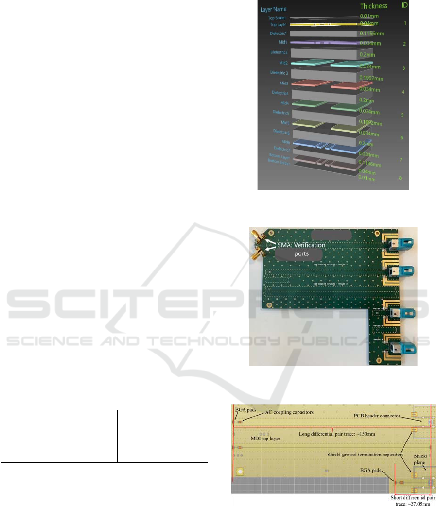
PCB would have a minimum of 8 layers. These layers
are also described in Figure 3 for the PCB design
concept defined in this study. Here, the layer stackup
is defined in a manner that targets a low signal IL
within the PCB MDI for the 25Gbps differential pair
traces. The dielectric materials used are designated in
Figure 3 as Dielectric1 through Dielectric 7. For three
separate 25Gbps PCB designs, a single dielectric
material (1 through 7) was selected with focus on a
low loss tangent as an essential parameter to ensure
low signal IL.
Table 2 shows the dielectric materials used within
this study based on the corresponding loss tangents at
10GHz.
Table 2: Overview of the dielectric materials and loss
tangents for 25Gbps PCB MDI design.
Dielectric Material
Loss Tangent,
@10GHz
Ro
g
ers
(
RO4003
)
0.0027
Me
g
tron6 0.0040
EM827
(
I
)
0.0280
Figure 4 provides an overview of the
implemented ECU PCB design for this study.
Multiple MDI differential pair traces are
implemented on a single PCB. All implemented PCB
designs originate from a single PCB panel.
The purpose of including the SubMiniature
version A (SMA) ports is described in Section 4.
ECU PCB MDI: this segment of the PCB is
defined in consideration of the overall ECU PCB
component spacing requirements. The MDI differential
pair trace lengths are typically designed in the range
between ~24mm through ~28mm. In this study two
Figure 3: Defined ECU PCB layer stackup from a design
tool.
Figure 4: Exemplary of the multiple implemented ECU
PCB MDI design test boards.
Figure 5: PCB MDI top layer description.
differential pair trace lengths have been defined. One
being ~27.05mm emulating an ECU PCB MDI case,
and a longer trace length of 150mm. Generally, the
higher the trace length the higher the signal IL (The
Sierra Circuits Team, 2021). Hence, the longer trace
length aids in further analyzing the MDI IL
25Gbps Automotive Ethernet ECU PCB: MDI Design Implementation and Insertion Loss Characterization
77

properties. On each differential pair trace, an
Alternating Current (AC) coupling capacitors of
100nF are included. A capacitive shield plane to
ground termination is also considered in the MDI
design. Refer to Figure 5 for a top layer description of
the PCB layout.
Furthermore, this study defines two MDI
differential trace layout structures to emulate typical
options of an ECU PCB design. These trace structures
are described in Figure 6 as Edge-Coupled Embedded
Microstrip (Str. A) and Edge-Coupled Stripline (Str.
B).
(a)
(b)
Figure 6: ECU PCB MDI trace structures: (a) Edge-
Coupled Embedded Microstrip and (b) Edge-Coupled
Stripline.
The MDI differential pair trace width and spacing
implemented vary with the dielectric material used as
well as the trace structure. The trace width considered
is 114µm and 133µm for Str. A and 101µm and 103µm
for Str. B. As for the differential pair trace spacing,
this is 135µm, 130µm, and 150µm for Str. A and
205µm, 210µm, and 230µm for Str. B. All differential
pair traces have a 100Ω impedance with a tolerance
of 10%.
4 MDI IL CHARACTERIZATION
This section is an extension of the analysis conducted
in (Borda J. J., 2022). Within this study, three MDI
IL characterization criteria for a 25Gbps Ethernet
transmission are defined. These criteria are based on
(1) the dielectric material (also according to the loss
tangent), (2) the differential trace structure and (3) the
differential trace length. MDI IL characterization is
conducted using the ECU PCB design concept in
accordance with the description in Section 3. For this,
mixed-mode S-Parameter test bench measurements
were conducted at room temperature conditions using
a 40GHz four-port Vector Network Analyzer (VNA).
The measurements were conducted with a start
frequency 𝑓
𝑠𝑡𝑎𝑟𝑡
of 1MHz and linear steps 𝑓
𝑠𝑡𝑒𝑝𝑠
of
1MHz (10000 linear points).
With the specified Nyquist frequency of 25Gbps
being at 7.03125GHz, the corresponding test stop
frequency 𝑓
𝑠𝑡𝑜𝑝
is set to 10GHz. IEEE 802.3cy
specifies MDI IL limits of up to 9GHz for a 25Gbps
Ethernet channel. For this study, the VNA is set for
an output power of -5dBm and Intermediate
Frequency (IF) Bandwidth (BW) to 1kHz (Borda J.
J., 2022) (IEEE 802.3cy (Unpublished), 2022).
As described in the test setup of the preceding
study in (Borda J. J., 2022), the measurements are
performed by setting 0.8mm pitch differential
precision test probes placed directly on the PHY BGA
pads (set I). For this study, the other end of the test
probes (set II) has a physical contact on the side of the
ECU PCB header connector pins (also refer to Figure
7). Both sides of the precision test probe cables are
then directly connected to a 40GHz VNA. The
specified IL for the precision differential test probes
used is less than ~3dB. However, de-embedding of
these test probes is performed also considering pin-
test probe contact mismatch (and probe length)
(Borda J. J., 2022).
Figure 7: Positioning of the differential precision test
probes on the MDI.
Additional verification measurements are
conducted using implemented SMA verification ports
(refer to Figure 4). These measurements serve the
purpose to validate the test conducted using the
precision differential test probes.
4.1 PCB Dielectric Material
Three variants of the PCB MDI test board designs
were implemented using the three different dielectric
materials defined in
Table 2. To ensure measurement
reproducibility, for each of these PCB MDI variants,
two DUTs were considered for the analysis.
Additionally, the two differential pair trace structures
Str. A and Str. B were considered separately on each
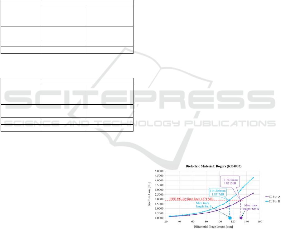
of the three PCB variants. Figure 8 displays the
outcome of the MDI IL at 7.03125GHz from the three
PCB variants with Str. A and Str. B on a ~27.05mm
differential pair trace length.
VEHITS 2023 - 9th International Conference on Vehicle Technology and Intelligent Transport Systems
78
(a)
(b)
Figure 8: Influence of PCB dielectric material on MDI IL:
(a) Trace Str. A and (b) trace Str. B.
In Figure 8 MDI IL variations between DUTs are
dependent on the dielectric material used and vary
between the values ~0.0175dB, ~0.0081dB, and
~0.0037dB. These variations between DUTs are
attributed to (1) PCB fabrication tolerances and (2)
tolerances in contacting the precision test probes onto
the PCB test regions. The influence of dielectric
material on MDI IL is dominated with EM827
followed by Megtron6 and lastly RO4003. These
observations are explained by their corresponding
loss tangents ( 𝐷
,
𝐷
,
𝐷
,
)
and their impact on the dielectric losses. The
maximum MDI IL in Figure 8 is based on EM927
with Str. B. Megtron6 and RO4003 exhibit lower
MDI ILs with a dependency on the differential pair
trace structure deployed. This dependency is further
discussed in Section 4.2.
4.2 MDI Differential Pair Trace
Structure
Based on the outcome of the three dielectric materials
on the MDI IL discussed in Section 4.1, this section
characterizes the individual impact of the differential
pair trace structures Str. A and Str. B on MDI IL using
the shorter trace lengths. Here, the maximum (max.)
MDI IL from each pair of DUTs for the same trace
structure is considered. These maximum MDI IL values
are summarized in Table 3 and Figure 9.
Table 3: Overview max. MDI IL based on varying MDI
differential pair trace structures.
Dielectric
Material
Max. DUT IL
@
7.03125GHz [dB]
Str. A Str. B
Rogers
(RO4003)
0.147 0.1795
Megtron6 0.2617 0.1438
EM827 0.6700 0.8272
Figure 9: Impact of MDI differential pair trace structures on
IL.
In terms of the impact of the differential pair trace
structures and independent of the dielectric material
used, in two cases Str. B exhibits higher MDI IL
values compared to Str. A. This is however with an
exception when Megtron6 dielectric material is
considered on the PCB design. The higher MDI IL on
Str. B is associated with conductor losses regarding
copper surface roughness with no radiation losses.
And in the case of an optimum 25Gbps Ethernet PCB
design, Str. B trace structure would additionally have
a copper plane to protect the differential trace pair
signal conductors from undesired signal crosstalk.
With this, Str. B is better suited for a 25Gps Ethernet
channel compared to Str. A. Furthermore, the
maximum MDI IL (0.872dB) for Str. B on a
27.07mm trace length lies within the specified limits
(< 1.8717 per 76.2mm trace) for a 25Gbps MDI.
4.3 MDI Differential Pair Trace
Length
Placement options for various required circuit
components are typically very limited in terms of
available space on the ECU PCB. This leads to cases
25Gbps Automotive Ethernet ECU PCB: MDI Design Implementation and Insertion Loss Characterization
79
were variations in MDI differential trace lengths
between different ECU implementations is expected.
This subsection characterizes the impact of the
MDI differential trace length on the MDI IL. Table 4
and Table 5 lists down the maximum measured MDI
IL at 7.03125GHz on the 150mm trace length based
on the two previously defined differential pair trace
structures (Str. A and Str. B) and the three dielectric
materials implemented in the design concept as per
Section 3.
Table 4: Max. MDI IL comparison at 7.03125GHz: Short
versus long differential pair trace for Str. A.
Dielectric
Material
Max. MDI IL [dB]
Short Trace
Length
(
27.05mm
)
Long Trace
Length
(
150mm
)
Rogers
(RO4003)
0.1477 2.9620
Me
g
tron6 0.2617 2.341
EM827 0.6570 7.2932
Table 5: Max. MDI IL comparison: Short versus long
differential pair trace for Str. B.
Dielectric
Material
Max. MDI IL [dB]
Short Trace
Length
(
27.05mm
)
Long Trace
Length
(
150mm
)
Rogers
(
RO4003
)
0.1795 4.9277
Me
g
tron6 0.1438 3.5855
EM827 0.8272 7.1115
The maximum MDI IL values in Table 4 and Table
5 are based on measurements conducted on two
DUTs of similar design type. Here, a comparison with
the corresponding implemented shorter differential
pair trace length (~27.05mm) is conducted. A higher
increase in MDI IL values is observed with Str. B due
to having an even higher increase in conductor losses
compared to Str. A (as addressed in Subsection 4.2).
With the maximum IEEE 802.3cy specified MDI
IL being at 1.8717dB for a 76.02mm differential pair
trace length, actual MDI design implementation tend
to exhibit variations due to non-ideal PCB
implementation aspects typically not considered in
such specifications. Based on the designed ECU PCB
MDI concept in this study, this subsection further
investigates the maximum possible MDI differential
pair trace length in correlation with the existing MDI
IL limit of 1.8717dB for a 25Gbps MDI. For this
characterization the following analysis approach is
defined within this study:
(1) At 7.03125GHz, for each PCB MDI design
variant with the three different dielectric
materials, the maximum MDI ILs based on
the two DUTs is plotted against the two
corresponding differential pair trace lengths
(27.05mm and 150mm).
(2) From (1) the graph trend line and the
governing equation is determined.
(3) The equations in (2) are then used to
determine additional maximum MDI ILs for
various differential pair trace lengths
considering the limit of 1.8717dB.
(4) The step in (3) is conducted for each PCB
MDI design variant and trace structure type
separately.
(5) From (4) a trend graph is determined on how
the MDI IL would vary dependent on how
the trace length will be chosen. It also
determines the trace length options
implementable to ensure compliance to the
limit of 1.8717dB.
As an outcome of the aforementioned analysis
and based on step (3), the governing equations for the
MDI ILs exhibit an exponential functional trend,
𝐼𝐿 𝐶𝑒
with 𝐶 being the function
coefficient. For Equation (4) through Equation (9),
the decimal function coefficients are rounded up to
one significant figure.
Figure 10 provides the range of the differential
pair trace lengths for an optimum 25Gbps MDI IL
with Rogers (RO4003) as the dielectric material. The
governing equations are described in Equation (4) for
Str. A and Equation (5) for Str. B. Here, 𝑇
stands for
differential pair trace length.
𝐼𝐿
,.𝑨,
𝑇
0.077𝑒
.
𝑑𝐵
(4)
𝐼𝐿
,.𝑩,
𝑇
0.087𝑒
.
𝑑𝐵
(5)
Figure 10: PCB MDI design variant with RO4003: Range
of MDI IL limit compliant differential pair trace lengths.
Figure 11 provides the range of the differential
pair trace lengths for an optimum 25Gbps MDI IL for
PCB MDI design variant with Megtron6 (Meg6) as
the dielectric material. The governing trend equations
are described in Equation (6) for Str. A and Equation
(7) for Str. B.
VEHITS 2023 - 9th International Conference on Vehicle Technology and Intelligent Transport Systems
80
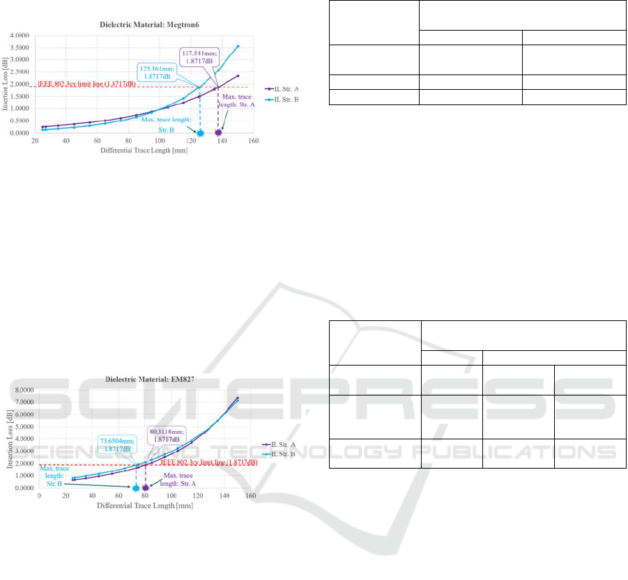
𝐼𝐿
,.𝑨,
𝑇
0.162𝑒
.
𝑑𝐵 (6)
𝐼𝐿
,.𝑩,
𝑇
0.071𝑒
.
𝑑𝐵
(7)
Figure 11: PCB MDI design variant with Megtron6: Range
of MDI IL limit compliant differential pair trace lengths.
Figure 12Figure 11 provides the range of the
differential pair trace lengths for an optimum 25Gbps
MDI IL for PCB MDI design variant with EM827 as
the last dielectric material. The governing trend
equations are described in Equation (8) for Str. A and
Equation (9) for Str. B.
𝐼𝐿
,.𝑨,
𝑇
0.387𝑒
.
𝑑𝐵
(8)
𝐼𝐿
,.𝑩,
𝑇
0.515𝑒
.
𝑑𝐵
(9)
Figure 12: PCB MDI design variant with EM827: Range of
MDI IL limit compliant differential pair trace lengths.
Table 6 summarizes the various maximum MDI
IL limit compliant differential pair trace lengths for
all the PCB MDI design variants defined within this
study. A trace length greater 76.02mm trace length is
implementable for Rogers and Megtron6 dielectric
materials. However, on the other hand, EM824 based
PCB MDI design variant exhibits significant lower
maximum trace lengths, with 80.3118mm for Str. A
and 73.6504mm for Str. B trace structures. This is
attributed to (1) the higher loss tangent of this
dielectric material compared to the remaining two and
consequently (2) the higher MDI IL that was already
obtained at a shorter trace length of 27.05mm.
Table 6: 25Gbps MDI IL limit compliant maximum
differential pair trace length.
Dielectric
Material
Max. trace length for MDI IL
< 1.8717dB at 7.03125GHz [mm]
Str. A Str. B
Rogers
(RO4003)
131.037 114.206
Me
g
tron6 137.541 125.361
EM827 80.3118 73.6504
4.4 Worst- and Best-Case MDI PCB
Design
Based on the characterization results in Sections 4.1,
4.2, and 4.3, this subsection defines and presents the
Worst-Case (WC) and Best Case (BC) ECU PCB
MDI design for a 25Gbps Ethernet communication
channel. Table 7 provides an overview.
Table 7: WC and BC ECU PCB MDI design parameters:
According to 25Gbps PCB MDI IL limit of 1.8717dB at
7.03125GHz.
Design
Parameter
Design for max. 1.8717dB MDI IL at
7.03125GHz
WC BC
Trace
Structure
Str. B Str. A Str. B
Dielectric
Material
EM827
Rogers
(RO4003)
Megtron6
Trace Length
[mm]
73.6504 131.037 125.361
In Table 7, the two BC ECU PCB MDI designs
provide more options for design variations. In this
case both Str. A and Str. B can be considered with
more flexibility in terms of the differential pair trace
length to be implemented. Though, application based,
mostly the trace lengths would be around ~28mm and
seldom beyond this value. As characterized in previous
subsections of this study, the WC ECU PCB MDI
design has a disadvantage in terms of the higher MDI
IL it exhibits even at shorter trace lengths of
27.05mm.
Overall, a dielectric material with a low loss
tangent (equal or less 0.0027) is recommended for a
25Gbps Automotive Ethernet MDI to attain an
optimum BC MDI IL similar to the characterized
cases for Rogers (RO4003) and Megtron6. As for the
differential pair trace structure selection, this will
depend on whether one goes for Roger (RO4003) or
Megtron6 design variant. Nevertheless, Str. B remains
preferable over Str. A due to its optimum overall high-
speed characteristics. (Coonrod , 2013).
25Gbps Automotive Ethernet ECU PCB: MDI Design Implementation and Insertion Loss Characterization
81
5 SIMULATIONS FOR ECU PCB
MDI IL CHARACTERIZATION
While test bench measurements are the standard
means for communication channel PHY validation
and qualification of “lower” (<10Gbps) data rates in
the automotive industry, reliable and meaningful
channel PHY simulations are not at all used at the car
manufacturers for this purpose, yet.
There are several existing and expected
challenges in terms of system level PHY test bench
validations and qualifications for beyond 10Gbps
in- vehicle connectivity. These primarily include (1)
tolerances in contacting the precision differential test
probes onto the PCB contact pads, (2) increased costs
on the required test infrastructure which includes
DUTs as well as test setup equipment, (3) more time
required to conduct the tests especially if multiple
DUTs have to be analyzed, and lastly (4) increased
measurement artifacts for high-speed signals
considering the steeper rise/fall signal timing
requirements and the impact of the additional
capacitance from the test probes on SI.
It is therefore imperative to conduct a feasibility
analysis for an alternative approach to validate and
qualify not only the PHY channel as a whole but
within this study, the ECU PCB MDI design. An
alternative aspect to be discussed is therefore the
usage of simulations in place of test bench
measurements. Essentially, this analysis focuses on
what simulations can cover and whether a full
replacement or coexistence with test bench
measurements is expected/reasonable within the
Automotive industry.
For this characterization, mixed-mode S-
Parameter analysis of the MDI differential pair trace
is performed using ANSYS SIwave and HFSS 3D.
Here, the same PCB MDI designs from
measurements in Section 4 are deployed.
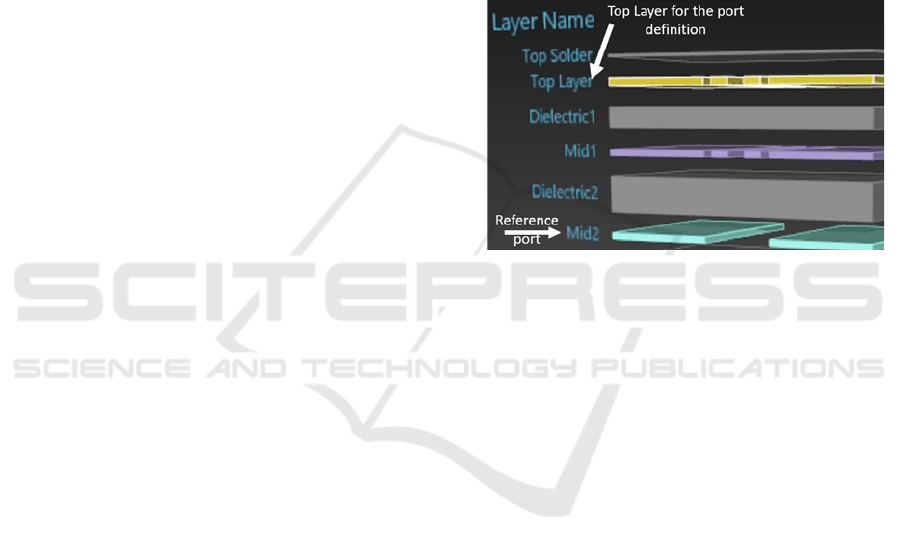
5.1 Ports and Reference Plane
The initial part of the analysis defines the reference
plane (also serving as the current return path) and
ports for the differential pair traces. To emulate actual
test bench measurement setup, the MDI simulation
ports are defined at the Top Layer (TL). The
corresponding reference ports are set at the mid 2
Layer (mid2). With the preference of a least
impedance (i.e., least inductance) path for high
frequency transmission, mid2 also serves as the
current return path for both Str. A and Str. B
(Archambeault, 2008).
In addition to an optimum selection of the MDI
AC coupling capacitance value, the Equivalent Series
Resistance (ESR) and Equivalent Series Inductance
(ESL) values play a key role. These values exhibit
ideal characteristics in a simulation compared to test
bench measurements. This is due to the actual
occurrence of the capacitor component tolerances on
actual test bench measurements. The ESR and ESL
are also influenced by the non-ideal characteristics of
the PCB layout, for instance, trace parameters and
dielectric constant variations (Borda J. J., 2022). The
study in (Borda J. J., 2022) provides a further
description of how the MDI port definition is
conducted for the simulation.
Figure 13: PCB layer selection for port and reference.
5.2 Correlation Between
Measurements and Simulations
As there are numerous variables to consider when
looking at the correlation between MDI IL test
measurements versus simulation, the question
remains, what is reasonable to compare between these
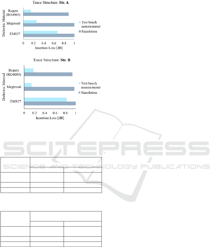
two. Figure 14 displays the MDI IL correlation
between test bench measurements and simulations for
Str. A and Str. B for a 27.05mm differential pair trace.
From Figure 14, independent of the dielectric
material used, MDI IL deviations between
simulations and measurements are observed. These
deviations vary between a minimum of 0.179dB and
a maximum of 0.8290dB.
Similar to test bench measurements, MDI IL from
simulations also exhibits an increase in value in this
particular order based on the dielectric material
Rogers (RO4003), Megtron6, and EM827. The
reason behind this trend was discussed in Section 4.1.
Table 8 and Table 9 provide an overview of the MDI
IL between simulations and measurements.
VEHITS 2023 - 9th International Conference on Vehicle Technology and Intelligent Transport Systems
82
(a)
(b)
Figure 14: PCB MDI IL trend correlation of measurements
versus simulations: (a) Trace Str. A and (b) trace Str. B.
Table 8: MDI IL: Simulation versus measurements for
Str. A.
Dielectric
Material
Simulation versus Measurements,
MDI IL Str. A [dB]
Simulations Measurements
Rogers
(RO4003)
0.8844 0.1470
Megtron6 0.9938 0.2617
EM827 1.0154 0.6700
Table 9: MDI IL: Simulation versus measurements for
Str. B.
Dielectric
Material
Simulation versus Measurements,
MDI IL Str. B [dB]
Simulations Measurements
Rogers
(
RO4003
)
0.9369 0.1795
Me
g
tron6 0.9728 0.1438
EM827 1.0063 0.8272
A higher valued MDI IL from measurements
leads to an improved correlation to simulation results.
Exemplary to this is with EM827. Whereas MDI IL
based on Rogers and Megtron6 exhibit high deviations
between simulations and measurements (refer to
Table 8 and Table 9).
The deviations in the observed MDI IL between
simulations and measurements can be attributed to
numerous factors. Primarily these factors include: (1)
Capacitance ESR and ESL variations between the
simulation model (ideal case) and actual non-ideal
capacitance used on the PCB MDI boards, (2)
tolerances in contacting measurement test probes
versus simulation port placement, (3) reference
ground used on the simulations can deviate to that
automatically used on measurements. On measurements
this is freely determined by a low impedance path and
not direct test probe placement. The definition of an
optimum reference ground addresses the most crucial
part of both simulation and measurements. This is
even more the case when dealing with Edge-Coupled
Embedded Microstrip trace structures where the vias
and transitions between multiple layers of the PCB
have to be considered.
Can simulations be deployed for 25Gpbs MDI IL
characterization? A general answer to this question is,
yes, however, the following conditions have to be
considered:
(1) Means to consider non-ideal characteristics
of the passive MDI components have to be
modelled as a standalone pre-analysis.
(2) Methodologies to correlate a test bench
versus simulation reference ground
definition throughout a trace structure have
to be defined.
(3) Baseline test bench measurements serve as
pre-requisite (i.e., coexistence).
(4) Only a non-quantitative comparison in terms
of the MDI IL trend between different
dielectric materials and design variants
provides a reasonable simulation analysis.
(5) Recommendable for designs with higher loss
tangent range based dielectric materials.
(6) With (3), MDI IL simulations are reasonable
for longer (70mm) differential pair trace
lengths. In this case, the high-speed
properties become even more visible.
6 CONCLUSION
For 25Gbps Automotive Ethernet connectivity, this
study has defined and characterized several essential
ECU PCB MDI aspects:
(1) Design concept for the PCB MDI.
(2) ECU PCB MDI IL budget characterization
using RF test bench measurements on the
design concepts based in (1).
(3) Feasibility of a simulation approach in
coexistence with RF test bench
measurements for MDI IL characterization.
25Gbps Automotive Ethernet ECU PCB: MDI Design Implementation and Insertion Loss Characterization
83

This study provides the baseline requirements and
specifications for the ECU PCB MDI system design
and implementation for 25Gbps in-vehicle
connectivity. Furthermore, this study serves as an
essential framework towards Automotive industry
standardization projects in regard to ECU PCB MDI
design and RF characterization as well as
qualification. Future studies are planned to
characterize signal attenuation in relation to crosstalk
on high densely populated 25Gbps ECU PCB MDI
design.
REFERENCES
Archambeault, B. (2008). Design Tip: Resistive versus
Inductive Return Current Paths, IEEE. Retrieved from
https://www.ewh.ieee.org/soc/emcs/acstrial/newsletter
s/spring08/design_tips.pdf
Borda, J. (2022). Which is more Suitable for Next
Generation Automotive Ethernet Connectivity: Copper
or Optical Fiber? Automotive Ethernet Congress .
Retrieved 06 2022
Borda, J. J. (2022). Beyond 10Gbps Electrical Automotive
Ethernet Channel Insertion. IEEE Intelligent Vehicles
Symposium. Aachen, Germany.
Coonrod , J. (2013). Insertion Loss Comparisons of
Common High Frequency PCB Constructions.
Retrieved January 2022, from Rogers Cooperation:
https://www.circuitinsight.com/pdf/insertion_loss_co
mparisons_pcb_constructions_ipc.pdf
Fan, W., Lu, A., Wai, L., & Lok, B. (2003). Mixed-Mode
S-Parameter Characterization of Differential
Structures. IEEE XPlore, 1,2,3. Retrieved January 23,
2022
IEEE 802.3ch. (2020). IEEE P802.3ch™: 2020, Standard
for Ethernet Amendment: Physical Layer
Specifications and Management Parameters for 2.5
Gb/s, 5 Gb/s, and 10 Gb/s Automotive Electrical
Ethernet. IEEE 802.3ch. Retrieved June 2022
IEEE 802.3cy (Unpublished). (2022, 07 01). IEEE
P802.3cy™/D2.0 Draft Standard for Ethernet
Amendment 9:Physical Layer Specifications and
Management Parameters for 25 Gb/s Electrical
Automotive Ethernet. Retrieved 08 2022, from
https://www.ieee802.org/3/cy/private/802.3cy_D2p0.p
df
Johnson, H., & Graham, M. (1993). High-Speed Digital
Design, A Handbook of Black Magic. Prentice Hall
PTR.
Knack, K. (2020, 10 06). https://resources.altium.com/.
Retrieved from https://resources.altium.com/p/increa
singly-important-role-loss-tangents-pcb-laminates
Mittal, A. (2021, March 8). Losses in PCB Transmission
Lines,https://www.protoexpress.com/blog/losses-in-
pcb-transmission-lines/. Retrieved January 23, 2022,
from https://www.protoexpress.com/blog/losses-in-
pcb-transmission-lines/
OPEN Alliance. ( 2020). 1000BASE-T1 EMC
Measurement Specification for Transceivers v2.1.
Retrieved 06 2022
OPEN Alliance. ( 2020). TC9, Channel and Components
Requirements for 1000BASE-T1 Link Segment Type A
(STP) v2.0. Retrieved 06 2022
OPEN Alliance. (2020). 1000BASE-T1 EMC
Measurement Specification for Transceivers v2.1.
Retrieved 06 2022
OPEN Alliance. (2022). TC9 (Unpublished) Channel and
Component Requirements for Fully Shielded
1000BASE-T1 and 2.5G/5G/10GBASE-T1 Link
Segments v0.7. Retrieved June 2022
Polar Instruments. (2022). AP8155 , https:// www.pola
rinstruments.com/support/si/AP8155.html. Retrieved
January 2022, from https://www.polarinstruments.com/
support/si/AP8155.html
The Sierra Circuits Team. (2021, 06 14). How to Reduce
Signal Attenuation in Hig-Speed PCBs. Retrieved from
https://www.protoexpress.com/: https://www.protoexp
ress.com/blog/how-to-reduce-signal-attenuation-high-
speed-pcbs/
VEHITS 2023 - 9th International Conference on Vehicle Technology and Intelligent Transport Systems
84
