
Practical Implementation of Diode SPICE Model with Reverse Recovery
Denys Igorovych Zaikin
a
Advent Technologies A/S, Lyngvej 8, Aalborg DK-9000, Denmark
Keywords:
Diode Reverse Recovery, SPICE, Circuit Simulation.
Abstract:
Peter O. Lauritzen and Cliff L. Ma proposed an approach for creating a physical model of reverse recovery
for soft recovery diodes in 1991. The current paper demonstrates how to create the proper SPICE sub-circuit
using only the specifications from the diode datasheet from the manufacturer. Software for characterization
tools has been developed, tested, and is now openly accessible for use.
1 INTRODUCTION
Of the many SPICE-based simulators on the market,
most still use the old standard diode SPICE model
that does not cover reverse recovery correctly. Both
LTspice (Analog Devices, Inc., 2008) and Pspice
(Cadence Design Systems, Inc., 2015) are powerful
pieces of software that are widely used for power elec-
tronics simulation. These SPICE simulators use a ba-
sic diode model. Adding a feature to simulate diode
reverse recovery will improve loss estimation and cir-
cuit behaviour simulation. This is especially attrac-
tive for LTspice, which is a powerful, free simulator
that can be used in complex design simulation. This
paper applies original theoretical work (Lauritzen and
Ma, 1991) to the practical implementation of a SPICE
macro model of diodes with reverse recovery. The
model described in (Lauritzen and Ma, 1991) is based
on real physical processes in a diode and, because of
this, is robust.
A Windows OS application was created to gener-
ate a diode macro model using only parameters from
the diode manufacturer’s datasheet or measurement
data.
2 DIODE MODEL DESCRIPTION
Original work (Lauritzen and Ma, 1991) provides the
following three equations for diodes with reverse re-
covery:
i(t) =
(q
E
− q
M
)
T
M
, (1)
a
https://orcid.org/0000-0003-4080-5631
0 =
dq
M
dt
+
q
M
τ
−
(q
E
− q
M
)
T
M
, (2)
q
E
= I
s
τ(e
(
v
nV
T
)
− 1). (3)
From equations (1)-(3), the forward DC-bias char-
acteristic can be obtained:
i =
I
s
(1 + T
M
/τ)
(e
(
v
nV
T
)
− 1). (4)
Here, i is the diode current, v is diode junction
voltage, V
T
= kT /q is the thermal voltage, I
s
is satura-
tion current (similar to the SPICE basic diode model
parameter) and n is the emission coefficient (similar
to the SPICE basic diode model parameter). The vari-
ables from (Lauritzen and Ma, 1991) are as follows:
T
M
represents diffusion time, τ recombination life-
time, q
M
total stored charge and q
E
charge variable.
This model is completed with ohmic resistance R
s
and
junction capacitance C
j
, as shown in Figure 1.
RS
D
CJ
Vf
v
i
Figure 1: Diode model components.
The practical implementation of equations (1)-(4)
in the SPICE model, along with ohmic resistance and
junction capacitance, are shown in Figure 2.
92
Zaikin, D.
Practical Implementation of Diode SPICE Model with Reverse Recovery.
DOI: 10.5220/0012096500003546
In Proceedings of the 13th International Conference on Simulation and Modeling Methodologies, Technologies and Applications (SIMULTECH 2023), pages 92-96
ISBN: 978-989-758-668-2; ISSN: 2184-2841
Copyright
c
2023 by SCITEPRESS – Science and Technology Publications, Lda. Under CC license (CC BY-NC-ND 4.0)

R1
{RS}
VALUE={-1/tau*V(qm)+V(qe,qm)/TM}
G1
C1
1
VALUE={Is*tau*(exp(V(C1,2)/(N*Vt))-1)}
E1
VALUE={V(qe,qm)/TM}
G2
R3
100G
D1
Cap
1
2
qe
qmC1
.param Temp_diode=1.250000e+002 k=1.381000e-023 q=1.602000e-019 Vt=3.430949e-002
.param Rs=2.196899e-002 Is=7.942178e-004 N=2.357317e+000 Tau=9.273759e-008 Tm=1.527752e-007
.param VJ=2.000000e+000 CJ0=9.311509e-010 M=6.974055e-001 FC=0.500000
.model Cap d (Is=1e-14 N=200 rs=10u Xti=0 Eg=0 CjO={Cj0} M={M} VJ={VJ} FC={FC})
Figure 2: Implementation of new diode model in SPICE.
3 EXTRACTION OF MODEL
PARAMETERS
Equations (1)-(3) fully describe diode reverse recov-
ery and DC bias characteristics of the diode. To use
these equations, it is necessary to define τ, T
M
, n and
I
s
parameters.
Parameters τ and T
M
are defined with the approach
used in (Lauritzen and Ma, 1991). An additional in-
termediate parameter – reverse recovery time constant
τ
rr
– is used and can be measured directly from the
reverse recovery waveform or defined from the diode
datasheet’s parameter T
rr
, the reverse recovery time.
Figure 3 shows the JEDEC Standard (JEDEC Stan-
dard No. 282B.01, 2000) definition of T
rr
.
Trr
1
e
I
RM
τ
rr
di
dt
t=0
t
T0
T1
I
F
i(t)
I
RM
0.25 I
RM
Figure 3: JEDEC reverse recovery time T
rr
definition and
waveform.
From Figure 3, τ
rr
can be found as follows:
τ
rr
= 0.75
I
RM
di
dt
− T
rr
!
1
ln(0.25)
. (5)
Now, when τ
rr
is known, parameters τ and T
M
can
be found using numerical equation solving of the fol-
lowing equations from reference (Lauritzen and Ma,
1991):
1/τ
rr
= 1/τ + 1/T
M
, (6)
I
RM
=
di
dt
(τ − τ
rr
)(1 − e
−
T 1
τ
). (7)
To find parameters I
s
, n and ohmic resistance R
s
in equation (4), the standard diode forward DC-bias
SPICE model equations are used (Figure 1):
V
f
= R
s
· i + v, (8)
i = I
′
s
· (e
v
nV
T
− 1). (9)
Based on Equation (9) and Figure 4, it can be seen
that I
s
’ is the leakage reverse current at the maximum
reverse voltage according to the datasheet’s reverse
DC-bias characteristic of the diode.
V
-I
s
'
V
f1
V
f2
I
d1
I
d2
1
2
Figure 4: DC-bias characteristic points.
Using Equations (4) and (9), I
s
can be found:
I
s
= I
′
s
· (1 + T
M
/τ). (10)
To find R
s
and n, two points should be defined
on the DC-bias diode characteristic (Figure 4). From
equations (8) and (9), there is system of equations
with two unknown variables, R
s
and n:
(
V
f 1
= n ·V
T
· ln(I
d1
/I
′
s
+ 1) + R
s
· I
d1
V
f 2
= n ·V
T
· ln(I
d2
/I
′
s
+ 1) + R
s
· I
d2
.
(11)
After system (11) is solved, R
s
and n are found:
n =
V
f 1
· I
d2
−V
f 2
· I
d1
ln
I
d1
I
′
s
+1
·I
d2
I
d2
I
′
s
+1
·I
d1
·
1
V
T
, (12)
R
s
=
V
f 2
−V
T
· n · ln(I
d2
/I
′
s
+ 1)
I
d2
. (13)
Practical Implementation of Diode SPICE Model with Reverse Recovery
93

To simulate non-linear junction capacitance, equa-
tions from the standard diode SPICE model are used
(Kielkowski, Ron M, 1995):
C
J
= C
J0
·
1 −
v
V
J
−M
, v < F
C
·V
J
, (14)
C
J
=
C
J0
(1 − F
C
)
M+1
×
1 − F
C
· (M + 1) +
M · v
V
J
, v ≥ F
C
·V
J
. (15)
In this model for junction capacitance, fixed parame-
ters are assumed: V
J
= 2.0 and F
C
= 0.5. It is also nec-
essary to find parameters M and C
J0
using two points
on the datasheet’s reverse bias capacitance curve in
Figure 5.
V
C
J
2
1
V
r1
V
r2
C
j2
C
j1
Figure 5: Junction capacitance points.
Using these two points, a system of equations can
be obtained based on Equation (14):
C
j1
= C
J0
·
1 +
V
r1
V
J
−M
C
j2
= C
J0
·
1 +
V
r2
V
J
−M
.
(16)
After (16) is solved, M and C
J0
can be found:
M =
ln
C
j1
C
j2
ln
1+V
r2
/V
J
1+V
r1
/V
J
, (17)
C
J0
= C
j1
·
1 +
V
r1
V
J
M
. (18)
To implement junction capacitance in the new
diode model, the standard SPICE diode model is
placed in parallel with the diode body (Figure 2).
The new diode SPICE model implements the be-
havior of the diode at a fixed temperature. Lead
inductances should be added externally for parasitic
simulation.
4 SIMULATION RESULTS
The newly generated model was tested in two simula-
tors – LTspice and Pspice. The LTspice IV simulation
results for the MUR460 diode are shown in Figure 6.
Figure 6: Comparison of current and standard waveform
LTspice IV simulation results for the MUR460 diode. The
MUR460 standard diode model was taken from the LT-
spice IV library.
Pspice 16.6 simulation results for the
HFA25TB60 diode are shown in Figure 7.
Figure 7: Comparison of current and standard waveform
Pspice 16.6 simulation results for the HFA25TB60 diode.
The HFA25TB60 standard diode model was taken from the
Pspice 16.6 library.
The Pspice 16.6 simulation results for ISL9R3060
diode are shown in Figure 8.
5 SOFTWARE DESCRIPTION
To generate the diode SPICE model using the man-
ufacturer’s datasheet characterization, the software
(SW) tool “DiodeRRSubmodel” was made (Figure 9).
It is a Windows OS application and can be freely
downloaded from the link (ZAIKIN D.I., 2021).
Next, input data from the datasheet are used as fol-
SIMULTECH 2023 - 13th International Conference on Simulation and Modeling Methodologies, Technologies and Applications
94
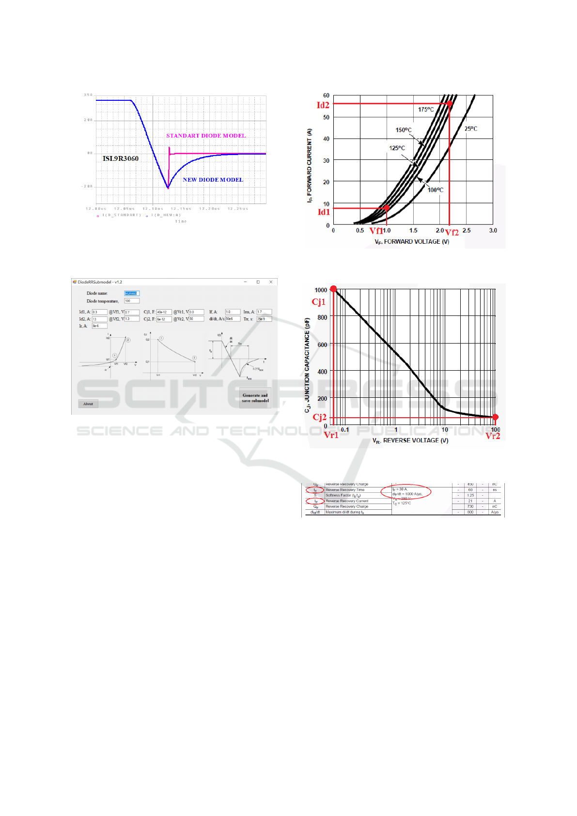
Figure 8: Comparison of current and standard waveform
Pspice 16.6 simulation results for the ISL9R3060 diode.
The ISL9R3060 standard diode model was taken from the
manufacturer webpage.
Figure 9: Windows OS application SW for diode model ex-
traction.
lows:
• user enters diode name;
• user defines work temperature of diode;
• user enters two points on the DC-bias forward
characteristic for the specified temperature (Fig-
ure 4, Figure 10). Points far enough away from
each other should be chosen;
• user enters reverse leakage current for diode at
specified temperature;
• user enters two points on the junction capacitance
(Figure 5, Figure 11). Points far enough away
from each other should be chosen;
• user enters the reverse recovery specification from
the diode datasheet at the specified temperature:
I
f
, di/dt, I
RM
, and T
rr
(Figure 3, Figure 12).
The extracted model file is placed in the same folder
as the .exe file of the SW. An example of a generated
netlist is shown in Figure 13.
Figure 10: Two points selected on the DC-bias characteris-
tic.
Figure 11: Two points selected on the junction capacitance
characteristic.
Figure 12: Reverse recovery datasheet’s specifications.
* Diode isl9r3060g2 A K
.subckt isl9r3060g2 1 2
.param Temp_diode=125 k=1.381E-23 q=1.602E-19 Vt=0.03430948
.param Rs=0.02156586 Is=0.0004614982 N=2.460456 Tau=5.909138E-08
+Tm=3.181049E-08
.param VJ=2 CJ0=9.311509E-10 M=0.6974055 FC=0.5
R1 C1 1 {RS}
G1 0 qm VALUE={-1/tau*V(qm)+V(qe,qm)/TM}
C1 qm 0 1
E1 qe 0 VALUE={Is*tau*(exp(V(C1,2)/(N*Vt))-1)}
G2 C1 2 VALUE={V(qe,qm)/TM}
R3 qm 0 100G
D1 C1 2 Cap
.model Cap d (Is=1e-14 N=200 rs=10u Xti=0 Eg=0 CjO={Cj0} M={M} VJ={VJ}
+FC={FC})
.ends isl9r3060g2
Figure 13: Generated netlist of new diode sub-model.
Practical Implementation of Diode SPICE Model with Reverse Recovery
95

6 CONCLUSION
In the work that is being presented, the diode SPICE
model is implemented together with an accurate sim-
ulation of reverse recovery. The study that is given
is based on the physical representation that was first
created in the source (Lauritzen and Ma, 1991). The
current work offers automated diode model develop-
ment based on datasheet specifications from the man-
ufacturer. Open source software is publicly accessi-
ble for diode characterisation and model generation
(ZAIKIN D.I., 2021).
REFERENCES
Analog Devices, Inc. (2008). LTspice - SPICE simulator
software. https://www.analog.com/en/design-center/
design-tools-and-calculators/ltspice-simulator.html.
Accessed 19-05-2023.
Cadence Design Systems, Inc. (2015). PSPICE - Circuit
Simulation. www.pspice.com. Accessed 19-05-2023.
JEDEC Standard No. 282B.01 (2000). Silicon Rectifier
Diodes.
Kielkowski, Ron M (1995). SPICE: Practical Device Mod-
eling. McGraw Hill.
Lauritzen, P. and Ma, C. (1991). A simple diode model
with reverse recovery. IEEE Transactions on Power
Electronics, 6(2):188–191.
ZAIKIN D.I. (2021). Software tool for the article: Prac-
tical implementation of diode SPICE model with re-
verse recovery. https://doi.org/10.6084/m9.figshare.
14912769. Accessed 19-05-2023.
SIMULTECH 2023 - 13th International Conference on Simulation and Modeling Methodologies, Technologies and Applications
96
