
Research on SVPWM and Midpoint Potential Balancing Algorithm
of Improved NPC Three-Level Inverter
Deng Pan
*
, Jun Gao and Yicai Liu
Wuhan Business University, Wuhan 430056, Hubei, China
Keywords: 24 Sectors, Modulation Method, Estimation-Simulation-Correction, Adjustment Factor, Balancing
Algorithm, Midpoint Potential.
Abstract: The traditional NPC three-level inverter SVPWM control adopts a 36-sector seven-segment modulation
method, which involves a large number of trigonometric functions and coordinate transformations. This
paper proposes a improved control strategy using 24 sectors, and introduces the SVPWM modulation
method and implementation steps in detail. Compared with the 36-sector control method, the workload of
calculation and table checking is significantly reduced. At the same time, this paper proposes a simple
"estimation-simulation-correction" midpoint potential balance control algorithm, through a large number
of simulation verification, extract the best adjustment factor k to adjust the action time of the starting
negative small vector and the redundant small vector, and realize the balance control of the midpoint
potential. Finally, the correctness of the proposed control method is verified by Simulink simulation.
1 INTRODUCTION
Medium and low voltage AC motor speed
regulation system generally adopts two-level
inverter topology, with SVPWM modulation
technology for motor stator flux tracking, the
method is easy to implement by digital controller,
compared with traditional SPWM technology, The
output current waveform is better, and the voltage
output of the inverter link is relatively stable. Since
the maximum withstand voltage value of a single
MOSFET switch transistor is generally not high
(≤600V). In the field of medium and high voltage
and high power,three-level inverter topology is
adopted, With the help of SVPWM modulation
technology,the output level number increases and
the output waveform quality is higher. In addition,
the three-level inverter topology has less voltage
switching stress for a single switch tube (Zhang,
2020; Li, 2016; Yang, 2018).
The implementation steps of the three-level
inverter topologySVPWM algorithm are the
division of large and small sectors, the judgment of
the switching vector action sequence of each sector,
the calculation of the switching vector action time,
and the calculation of modulation fuze value.
Model establishment relies on a large number of
trigonometric operations and table queries (Li,
2016; Yang, 2018), and the frequent operation of
the switch tube will increase the disturbance of the
system, resulting in a decrease in control
performance and an increase in the harmonic
component of the output waveform (Zhang, 2020).
Literature (Zhang, 2020) proposes an improved
36-sector seven-segment modulation method,
which uses the coordinate translation method to
correct the reference voltage vector, but due to the
large number of sectors, the overall calculation
amount is large.Literature (Wang, 2022) proposes a
transformation method for split-inductive
three-level inverter.It reduces the performance
impact of short circuits on the circuit.Literature
(Zhao, 2008) introduces a three-level inverter
SVPWM method in 60° coordinate system, which
reduces sector judgment and trigonometric
operation from 36 sectors to 24 sectors, saving the
operation time, However, there are few textual
descriptions of the pulse-width modulation strategy
of the above methods. Literature (Wang, 2010)
introduces an LCL filter design method, The total
inductance value of the LCL filter can be
determined by the power supply power conditions
and ripple suppression requirements, and on this
basis, the inductance ratio and filter capacitance
value can be determined. The NPC three-level
topology has the problem of midpoint potential
imbalance, which is a difficult point to study the
structure. Literature (Song, 2004) provides a
Pan, D., Gao, J. and Liu, Y.
Research on SVPWM and Midpoint Potential Balancing Algorithm of Improved NPC Three-Level Inverter.
DOI: 10.5220/0012142200003562
In Proceedings of the 1st International Conference on Data Processing, Control and Simulation (ICDPCS 2023), pages 5-16
ISBN: 978-989-758-675-0
Copyright
c
2023 by SCITEPRESS – Science and Technology Publications, Lda. Under CC license (CC BY-NC-ND 4.0)
5
potential control method for injecting zero vector,
due to the different zero vector injection order in
different sectors, This method needs to first
determine the sector number, and then look up the
table to obtain the zero vector action time.
Literature (Fan, 2015) proposes to use optimization
of the last three virtual vectors to control the
midpoint potential balance. This method adopts
more approximation processing in the process of
virtual vector calculation, the cumulative error is
large. Literature (Ovalle, 2017) proposes to use two
adjacent small vectors to equivalently synthesize
medium vectors to adjust the action time of small
vectors and redundant small vectors. However, the
synthesized medium vector is composed of
asymmetric small vectors, and the influence of
small vectors on the midpoint potential cannot be
ignored. Literature (Song, 2012) provides a
closed-loop bidirectional buck-boost converter to
compensate for the impact of load disturbance on
the DC side voltage, which is theoretically mature.
However, BUCK/BOOST circuits need to be added,
and hardware and maintenance costs increase.
This paper proposes an SVPWM control
algorithm based on 24-sector improved NPC
three-level inverter, and introduces the SVPWM
modulation method and implementation steps in
detail.At the same time, a simple
"Estimation-simulation-correction" midpoint
potential balance algorithm is proposed, and the
optimal regulatory factor is extracted as the input
quantity for the time control of the initial negative
small vector and the redundant small vector
through a large number of simulation verification.
Finally, simulation is carried out to verify the
correctness of the above algorithm and control
strategy.
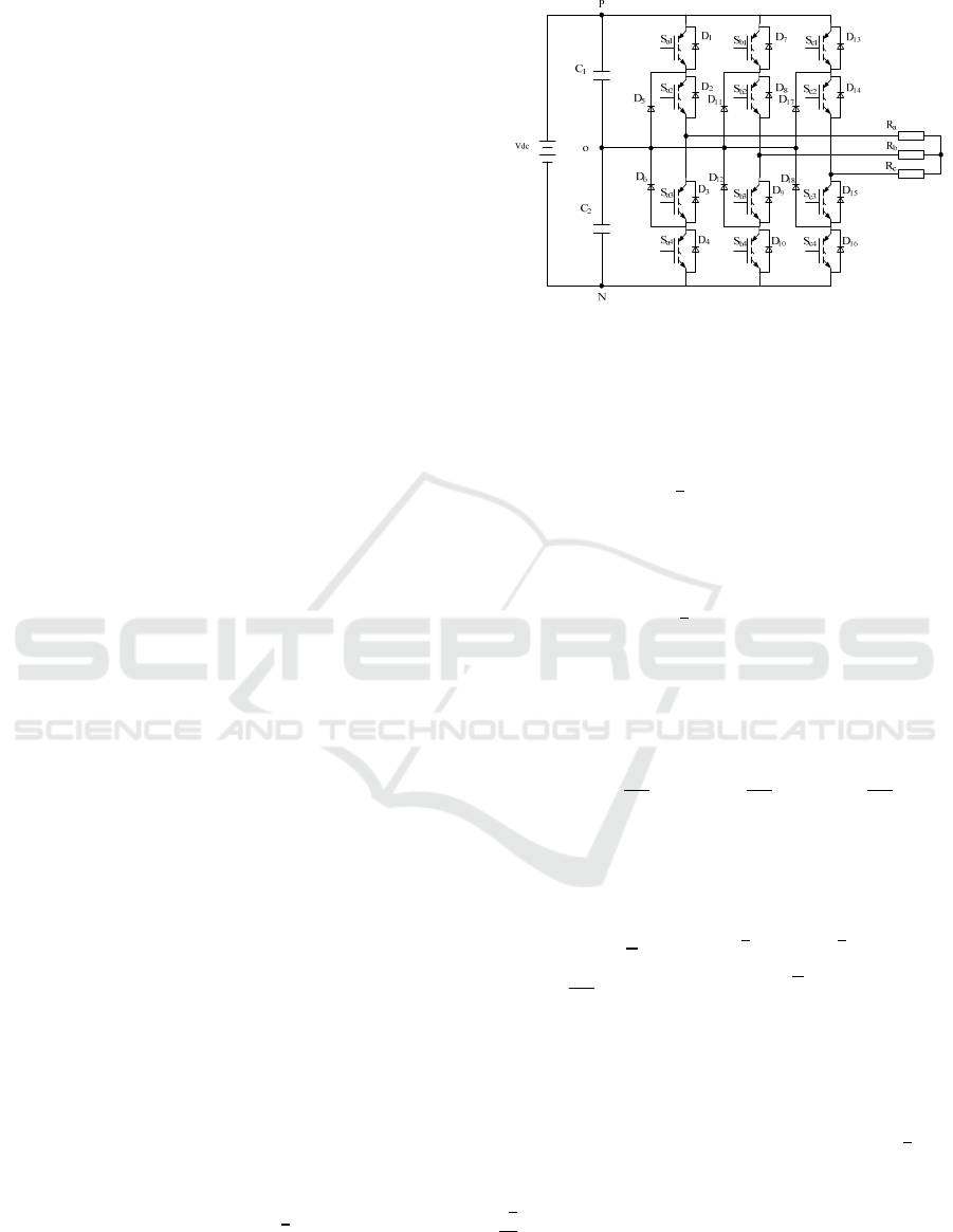
2 NPC THREE-LEVEL CIRCUIT
TOPOLOGY ANALYSIS
Figure 1 shows the topology diagram of the NPC
three-level circuit,Figure V
dc
is the DC-side supply
voltage,C
1
and C
2
are the DC side regulator
capacitor, D
5
、
D
6
、
D
11
、
D
12
、
D
17
、
D
18
are clamp diode
for A
、
B
、
C phase. Sa
1
~Sa
4
、
Sb
1
~Sb
4
、
Sc
1
~Sc
4
are
switch tubes,o is the neutral point on the DC
side.Since the regulator capacitors C1 and C2 are
equal, so there is 𝑈𝑐
= 𝑈𝑐
=
𝑉
.
Figure 1: NPC three-level circuit topology diagram.
Each phase bridge arm can output three
different levels,Define 𝑆
、
𝑆
、
𝑆
as three-leg
switch state variables,Take phase 𝐴 as an
example, 𝑆
、
𝑆
conduction, 𝑆
、
𝑆
disconnection,𝑈
=
𝑉
,
𝑆
=1 ; 𝑆
、
𝑆
conduction, 𝑆
、
𝑆
disconnection, 𝑈
=0 , 𝑆
=0 ; 𝑆
、
𝑆
disconnection,𝑆
、
𝑆
Conduction, 𝑈
= −
𝑉
, 𝑆
= −1 ,And 𝑆
and
𝑆
are in opposite states; 𝑆
and 𝑆
are in
opposite states.
The output state of bridge arms 𝐴
、
𝐵
、
𝐶 is
represented by switch function, Define three-phase
voltage as (Liu, 2012; Dang, 2016):
𝑈
=
𝑆
;
𝑈
=
𝑆
;
𝑈
=
𝑆
(1)
Equal amplitude transformation of three-phase
synthetic voltage vector, And expansion by Euler
formula:
𝑈=
2
3
𝑈
+ 𝑈
𝑒
+ 𝑈
𝑒
=
[(2𝑆
−𝑆
−𝑆
)+𝑗
√
3(𝑆
−𝑆
)] (2)
Combined (1, 2), 27 kinds of space voltage vectors
can be obtained, As shown in Figure 2. Four
voltage vectors can be obtained by ordering the
vector amplitude from large to small.
(1) The amplitude of large vector is
𝑉
,
For example:1 -1 -1;
(2) The amplitude of Medium vector is
√
𝑉
, For example:1 0 -1;
ICDPCS 2023 - The International Conference on Data Processing, Control and Simulation
6
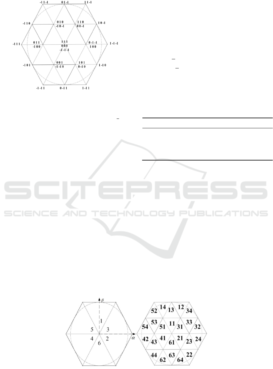
Figure 2: Basic vector diagram of NPC three-level
inverter.
(3) The amplitude of Small vector is
𝑉
,
Small vectors are divided into positive small
vectors and negative small vectors. For example, 1
0 0 is a positive small vector, 0 -1 -1 is a negative
small vector;
(4) The zero vector amplitude is 0, such as 1
1 1 (Hu, 2017; Zhang, 2018; Wang, 2002).
3 ANALYSIS OF CONTROL
ALGORITHM BASED ON 24
SECTORS
3.1 Division of Large and Small Sectors
In order to guide the target flux to form a quasi
circular track, the voltage vector should be
switched to the appropriate sector at an appropriate
time, and the sector number must be agreed
first.Through Clarke transformation, three-phase
static 𝐴
、
𝐵
、
𝐶 coordinate systems can be
converted to two-phase static 𝛼
、
𝛽 coordinate
systems, As shown in Figure 3.The components
𝑈
、
𝑈
、
𝑈
of the rotation vector on the
𝐴
、
𝐵
、
𝐶 axes can be represented by the
components 𝑈
、
𝑈
of the reference vector in the
two-phase stationary coordinate system.
Define variables 𝑎
、
𝑏
、
𝑐,And make rules:
(1) If 𝑈
>
0, 𝑎=1, otherwise 𝑎=0;
(2) If
√
3
𝑈
−𝑈
>
0, 𝑏=1, otherwise 𝑏=0;
(3) If −
√
3
𝑈
−𝑈
>
0, 𝑐=1, otherwise 𝑐=0;
Define 𝑁 as the large sector code, Take 𝑁=
𝐴+2𝐵+4𝐶, Table 1 shows the numbering rules of
large sectors (Zhang, 2018; Wang, 2002).
Table 1: Table of large sector numbering sequences.
Large sector
1
2
3
4
5
6
𝑎
1
0
1
0
1
0
𝑏
0
1
1
0
0
1
𝑐
0
0
0
1
1
1
Each large sector can be equally divided into
four small sectors, and 𝑛 is defined as the number
of small sectors, As shown in Figure 4,That is,
11~14 sectors, 21~24 sectors, 31~44 sectors, 41~44
sectors, 51~54 sectors, 61~64 sectors, A total of 24
small sectors.Next, It is necessary to determine the
position relationship between the target vector 𝑉
⃗
and the small sector.Taking the third sector as an
example, define the included angle between 𝑉
⃗
and 𝛼 axis as 𝜃,Then the component of 𝑉
⃗
on
coordinate axis 𝛼
、
𝛽 is:
𝑉
′
= 𝑉
× 𝑐𝑜𝑠𝜃
𝑉
′
= 𝑉
×sin𝜃
(3)
Figure 3: Large sector numbering chart. Figure 4: Small sector numbering diagram.
Research on SVPWM and Midpoint Potential Balancing Algorithm of Improved NPC Three-Level Inverter
7

Table 2: Table of voltage vector action order of small sectors.
Small Sector
𝑇
/4 𝑇
/2 𝑇
/2 𝑇
/2
𝑇
/2 𝑇
/2 𝑇
/4
31
0 -1 -1 0 0 -1 0 0 0 1 0 0
0 0 0
0 0 -1
0 -1 -1
32
0 -1 -1 1 -1 -1 1 0 -1 1 0 0
1 0 -1
1 -1 -1
0 -1 -1
33
0 -1 -1 0 0 -1 1 0 -1 1 0 0
1 0 -1
0 0 -1
0 -1 -1
34
0 0 -1
1 0 -1
1 1 -1
1 1 0
1 1 -1
1 0 -1
0 0 -1
It is easy to get the judgment
conditions:(1) 𝑉
+
√
𝑉
<
, 𝑛=31; (2) 𝑉
−
√
𝑉
>
, 𝑛=32; (3) 𝑉
>
√
, 𝑛=34;
(4)Otherwise, 𝑛=33. For the other five large
sectors, when judging the corresponding small
sector, it is only necessary to convert angle a to
sector 3.
3.2 Determine the Switching Sequence
of Small Sectors
The operation rule of SVPWM is to determine the
three basic output space vectors according to the
space sector position of target voltage vector 𝑉
⃗
,
and calculate the action time of each basic vector.In
order to reduce the voltage stress of the switch as
much as possible, the adjacent negative small
vector of voltage vector 𝑉
⃗
is preferred as the
starting vector. According to the above rules, the
basic voltage vector of each small sector and the
vector action sequence are shown in Table 2 (only
the switching sequence of the third largest sector is
listed in the table, see Appendix 1 for details).If the
target voltage vector 𝑉
⃗
is in sector 31, the three
basic vectors selected for synthesis are 0 -1 -1、0 0
-1、0 0 0.The action time of each basic vector is
、
、
、
、
、
、
.
3.3 Determine the Action Time of
Three Basic Vectors
Figure 5: Third largest sector.
Take 31 sectors for example, The three basic
voltage vectors of the synthetic target voltage
vector 𝑉
⃗
are defined as 𝑉
⃗
、
𝑉
⃗
、
𝑉
⃗
, 𝑇
、
𝑇
、
𝑇
is the base vector response time, 𝑇
is the
sampling period,From the principle of volt-second
balance:
𝑉
⃗
𝑇
+ 𝑉
⃗
𝑇
+ 𝑉
⃗
𝑇
= 𝑉
⃗
𝑇
𝑇
+ 𝑇
+ 𝑇
= 𝑇
(4)
31 Sector Base Vector Voltage:
𝑉
=0,𝑉
=
𝑉
, 𝑉
=
𝑉
𝑒
(5)
The combination formula (4, 5) yields:
0+
𝑉
𝑇
+
𝑉
𝑒
𝑇
= 𝑉
𝑒
𝑇
(6)
Define intermediate variables
𝑚=
√
×
× 𝑇
,
It can be solved:
𝑇
= 𝑚𝑠𝑖𝑛(60−𝜃)
𝑇
= 𝑚𝑠𝑖𝑛𝜃
𝑇
= 𝑇
−𝑚𝑠𝑖𝑛( 𝜃+ 60)
(7)
Similarly, the basic vector action time for each
small sector can be solved as shown in Table 3
(only the basic vector action time for the third
largest sector is listed in the table, See Appendix 2
for details):
ICDPCS 2023 - The International Conference on Data Processing, Control and Simulation
8

Table 3:
Timeline of basic vector action for each sector.
Small sector
𝑇
Time of action 𝑇
Time of action 𝑇
Time of action
31
𝑚𝑠𝑖𝑛(60−𝜃) 𝑚𝑠𝑖𝑛𝜃 𝑇
−𝑚𝑠𝑖𝑛(60+𝜃)
32
2𝑇
−𝑚𝑠𝑖𝑛(60+𝜃) 𝑇
−𝑚𝑠𝑖𝑛(60−𝜃) 𝑚𝑠𝑖𝑛𝜃
33
𝑇
−𝑚𝑠𝑖𝑛𝜃 𝑇
−𝑚𝑠𝑖𝑛(60−𝜃) −𝑇
+ 𝑚𝑠𝑖𝑛(60+𝜃)
34
𝑚𝑠𝑖𝑛(60−𝜃) −𝑇
+ 𝑚𝑠𝑖𝑛𝜃 2𝑇
−𝑚𝑠𝑖𝑛(60+𝜃)
3.4 Determine Switch Fuse Value
In order to minimize the harmonic component of
the output voltage of the inverter, a seven-segment
symmetric SVPWM modulation is usually used,
that is, the inverter outputs seven voltage vectors in
one switch cycle (Song, 2012). Figure 6 shows a
method to determine the switch start time. An
isosceles triangle is generated by the counter and
compared with a constant value to determine the
switch time. The constant value mentioned here is
the switch fuse value.
Figure 6: The corresponding diagram of the switching
time.
The seven time periods in the figure correspond to
six switch moments. The input moments of each
vector can be obtained by comparing the three
switch fuses
𝐴
、
𝐵
、
𝐶
in the figure with the
triangular wave.The amplitude of the triangle wave
in the graph is set to
, Period set to
𝑇
.When
the projection value of the triangular wave output
on the
𝑌
axis is in the range of 0-
𝐴
, the
corresponding vector trigger time is
.When the
projection value is within
𝐴
~
𝐵
range, the
corresponding vector trigger time is
(
+
)
,
When the projection value is within
𝐵
~
𝐶
range,
the corresponding vector trigger time is
(
+
+
)
,Therefore, the value of
𝐴
、
𝐵
、
𝐶
should
meet the following relationship:
⎩
⎪
⎨
⎪
⎧
𝐴=
𝐵= 𝐴+
=
+
𝐶= 𝐵+
=
+
+
(8)
Taking three sectors as an example, the comparison
relationship between the basic vector action time
and the switch state is shown in Figure 7. The
three-phase vector state corresponds to all the
switch states. The switching on and off times of the
switch devices are allocated to the corresponding
switch devices to complete the selection of the
main circuit switch devices.
Table 4 shows the trigger time table of
switching devices in each small sector (only the
third largest sector is taken as an example in the
table, see Appendix 3 for details).Define variable
𝑋=
, 𝑌=
+
, 𝑍=
+
+
, As the switch
status of the bridge arms of each phase is opposite
to each other, the table only lists the trigger time of
the two switches on the upper layer of each bridge
arm.In addition, if the state value in the table is 1, it
means that the switch cycle is high level, otherwise
it is low level.
Research on SVPWM and Midpoint Potential Balancing Algorithm of Improved NPC Three-Level Inverter
9

4
0
T
2
1
T
2
2
T
2
0
T
2
2
T
2
1
T
4
0
T
4
0
T
2
1
T
2
2
T
2
0
T
2
2
T
2
1
T
4
0
T
4
0
T
2
1
T
2
2
T
2
0
T
2
2
T
2
1
T
4
0
T
4
0
T
2
1
T
2
2
T
2
0
T
2
2
T
2
1
T
4
0
T
Figure 7: Seven-segment SVPWM modulation waveform (taking sector 3 as an example).
Table 4: Switching device trigger schedules for each sector.
𝑛
𝑆
𝑆
𝑆
𝑆
𝑆
𝑆
31
1 0
𝑋
0
𝑌
32
𝑋
1 0
𝑌
0
33
𝑌
1 0
𝑋
0
34
𝑋
1
𝑌
1 0
Figure 8: SVPWM control simulation model of a 24-sector NPC three-level inverter.
3.5 Simulation Verification
The simulation model built by Simulink is shown in
Figure 8, and the parameter settings are as follows:
the DC side voltage of the inverter 𝑉
is 500V,
the expected inverter output a rotation voltage
vector with a period of 0.02s and amplitude of
180V, and the defined cycle sampling frequency
𝐹
is 1e4Hz, and the sampling period 𝑇
is
1e-4s; The three-phase symmetrical load resistance
is 100𝛺, the inductance 𝐿
is 16e-6H, and the
capacitance 𝐶 is 16e-6F;The DC side voltage
stabilizing capacitor 𝐶
、
𝐶
is 500e-6F.Powergui
adopts Discrete mode, and the system sampling
frequency is set to 20 times of the periodic
sampling frequency.
Z
Z
Z
Z
ICDPCS 2023 - The International Conference on Data Processing, Control and Simulation
10
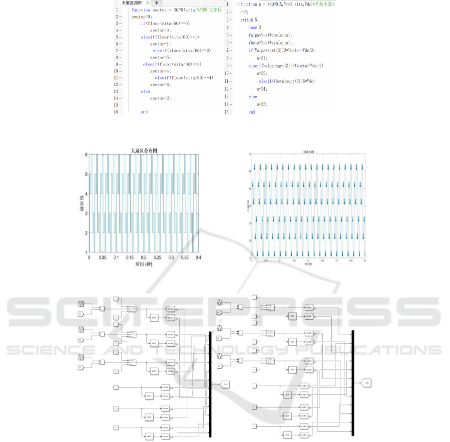
Figure 9: S-Function is used to determine large and small sectors.
Figure 10: Distribution of large sectors. Figure 11: Distribution of small sectors.
Figure 12: Sectors 31 and 32 judge the switching time
The S-Function function is used to judge the large
and small sectors, as shown in Figure 9. For the
judgment of small sectors, only the judgment
method of the third sector is listed in the figure, and
the judgment method of other sectors is the same.
Figure 10 and Figure 11 show the distribution of
large and small sectors after operation.
Figure 12 shows the judgment statement for the
trigger time of sector 31 and 32 switches. The
three-level SVPWM modulation trigger pulse can
be obtained by comparing the switch fuse value
with the Y-axis projection value of the modulated
triangle wave and strictly comparing the trigger
schedule of the switching devices in each sector
(Appendix 3). Set the simulation environment of
Simulink. The simulation start time is 0s and the
end time is 0.4s. Fixed step is adopted and Discrete
mode is adopted for the algorithm.
Research on SVPWM and Midpoint Potential Balancing Algorithm of Improved NPC Three-Level Inverter
11

Figure 13: Load phase voltage waveform Figure 14: Load line voltage waveform.
电容C1电压值
电容C2电压值
Figure 15: Capacitor C1 and C2 voltage values. Figure 16: Voltage difference between capacitors C1 and C2.
Figure 13 and Figure 14 are waveform diagrams of
three-phase load phase voltage and line voltage
respectively. The waveform period is 0.02s, in
which the amplitude of phase voltage is
𝑉
, and
there are
𝑉
and
√
𝑉
voltage vectors in the
waveform; The line voltage amplitude is 𝑉
, and
there are 𝑉
and
𝑉
voltage vectors in the
waveform. The simulation waveform further
verifies the conclusion in 2.1.
4 A SIMPLE MIDPOINT
POTENTIAL BALANCE
ALGORITHM BASED ON
"ESTIMATION-SIMULATION-
CORRECTION"
Further verify the influence of the above SVPWM
algorithm on the neutral point potential of the
inverter. Measure the two capacitor voltages and
the neutral point voltage of the DC bus respectively,
extend the simulation time to 2s, and obtain curves
as shown in Figures 15 and 16. After the simulation
starts, the voltage values of 𝐶
、
𝐶
capacitors are
roughly the same, the midpoint voltage is about 0V,
and there is almost no zero shift at the moment of
starting. The simulation lasts for 0.5s, the voltage
value of 𝐶
capacitor is about 260V, the voltage
value of 𝐶
capacitor is about 240V, The
differential pressure at both ends of capacitor 𝐶
and 𝐶
is about 20V. As time goes on, the offset of
the midpoint voltage increases, and the distortion of
the line voltage is obvious, which will interfere
with the steady state performance of the system
(Fan, 2015; Dang, 2016). When paired small
vectors act on the midpoint, they produce the same
line voltage, but their current values have the
opposite effect on the midpoint voltage,
counteracting part of the voltage imbalance (Zhang,
2018). To achieve a balanced control of the
midpoint potential, the action time of negative
small vectors and redundant small vectors can be
allocated (Jiang, 2014). An adjusting factor 𝑘 is
introduced to modify the on-off fuse of the starting
negative and redundant small vectors, thus
changing the on-off time of the switch tube.
Analyzing Figure 1, when the current flows
into the bus, when 𝑖
<
0, 𝐶
is discharged, and 𝐶
is charged, the midpoint potential has an upward
trend; Conversely, 𝑖
>
0, 𝐶
charge, 𝐶
discharge,
midpoint potential has a downward trend (Song,
2004). The S-Function function is used to
determine the value of the pair, and the input
amount is the voltage difference of capacitors 𝐶
、
𝐶
(𝑉
in the figure) and the current flowing
in/out of the DC bus.
ICDPCS 2023 - The International Conference on Data Processing, Control and Simulation
12

Figure 17: The value of the capacitor voltage. Figure 18: Capacitor voltage difference.
The method of "Estimation-simulation -correction"
is adopted, and different parameters are estimated
respectively, verified by a large number of
simulations, and the obtained values are corrected.
The simulation results show that when 𝑖
>
0
and 𝑉
>
0 , 𝑘=0.7; when 𝑖
>
0 and 𝑉
<
0 ,
𝑘=0.3; when 𝑖
<
0 and 𝑉
>
0, 𝑘=0.3; when
𝑖
<
0 and 𝑈
<
0, 𝑘=0.7, In this way, the offset
suppression effect of the midpoint voltage of the
DC bus is better. After the 𝑘 value is introduced,
equation (8) is modified to obtain an optimized
switch fuze as shown in equation (9):
⎩
⎪
⎨
⎪
⎧
𝐴=
×
(
1+0.7
)
𝐵= 𝐴+
=
+
𝐶= 𝐵+
=
×(1−0.7) +
+
(9)
Modify the model parameters according to equation
(9), and the simulation time is extended to 6s, and
the voltage difference and midpoint voltage
waveform of the DC bus capacitor are shown in
Figures 17 and 18. In Figure 17, the stability value
of the DC side power supply 𝐶
is about 251V, the
stability value of 𝐶
is about 248V, and the voltage
difference between the readout capacitors 𝐶
、
𝐶
in Figure 18 is about 3V, and it tends to stabilize
over time, The simple algorithm better suppresses
the fluctuation of midpoint potential.
5 CONCLUSION
Based on the traditional 36 sector SVPWM control
algorithm, this paper proposes an improved 24
sector SVPWM control algorithm, and introduces
the modulation method and implementation steps of
this algorithm in detail. At the same time, a simple
"Estimation-simulation-correction" neutral point
potential balance control algorithm is proposed, and
the value method of regulating factor k is
introduced, as well as how to use the value of k to
allocate the action time of negative small vectors
and redundant small vectors. A simulation model is
built to verify the above algorithm. Combined with
the simulation results, the correctness of the
proposed control algorithm is proved.
ACKNOWLEDGEMENT
Fund: Wuhan Business College University-level
Scientific Research Project (2021KY017).
REFERENCES
Zhang Yunlei, Wang Qunjing, Hu Cungang, et al.
Research on a new low-voltage non isolated 17 level
converter and its control strategy. Chinese Journal
of Electrical Engineering, 2020, 40(4):1095-1105.
KAI Li, ZHAO Jiancheng,WU Wenjie. Performance
analysis of zero common‐mode voltagepulse‐width
modulation techniques for three ‐ level neutral point
clamped inverters. IET Power Electronics, 2016,
9(14):2654-2664.
Yang Yun,Tan Siew-Chong,Hui Shu Yuen Ron. Adaptive
reference model predictive control with improved
performance for voltage-source inverters. IEEE
Trans on Control Systems Technology, 2018, 26(2):
724-731.
Wang Xiaobiao, Xiao Huaping, Niu Chenhui, Yao
Zhongyuan, Xiao Huafeng. Research on the
construction method of highly reliable three-level
inverter. Chinese Journal of Electrical Engineering,
2022, 25 (4):839-849.
Song Qiang, Liu Wenhua, Yan Gangui, Wang Zhonghong.
Neutral point potential balance control method of
three-level NPC inverter based on zero sequence
voltage injection. Chinese Journal of Electrical
Engineering, 2004, 05(6):52-62.
Zhao Hui, Li Rui, Wang Hongjun, Yue Youjun. Research
on SVPWM method of three-level inverter in
60°coordinate system. Chinese Journal of Electrical
Research on SVPWM and Midpoint Potential Balancing Algorithm of Improved NPC Three-Level Inverter
13

Engineering, 2008, 30(5):405-413.
Wang Fusheng, Shao Zhang, Ping Liuping. Current
ripple analysis and LCL filter design of three-level
inverter. Power Electronics Technology, 2010,
44(11):76-84.
Ovalle A., Hernández M. E. Nonorthogonal-
Reference-Frame-Based SVPWM Framework for
Multilevel Inverters. IEEE Transactions on Power
Electronics, 2017, 32(6):4925-4938.
Fan Bo, Zhao Weigang, Liu Gang, Xie Dongdong Closed
loop control of neutral point potential balance of
three-level inverter based on optimized virtual
vector. Journal of Electrical Technology, 2015,
30(04):124-132.
Song Wensheng, Feng Xiaoyun. Internal relationship
between a single-phase three-level SVPWM
modulation and carrier SPWM. Journal of
Electrical Technology, 2012, 27(6):131-138.
Jiang Haipeng, Liu Yongqiang. Simplified SVPWM
double closed loop control of VIENNA rectifier
with neutral point potential balance control. Journal
of Motor and Control, 2014, 18(2):35-41. DOI:
10.15938/2014.02.007.
Liu Sensen, Li Bin, Hang Lijun, etc A new control
method of VIENNA rectifier when three-phase
power network is unbalanced. Chinese Journal of
Electrical Engineering, 2012, 32(21):54-62. DOI:
10.13334/j.0258-8013. pcsee. 2012.21.009.
Dang Chaoliang, the same as Qianfeng, etc. Proportional
repetitive control of Vienna rectifier based on
equivalent carrier SVM. Power Electronics
Technology, 2016, 50(12):59-62+70. DOI: CNKI:
SUN: DLDZ. 0.2016-12-021.
Hu Cungang, Ma Dajun, Wang Qunjing, et al. Loss
distribution balance control strategy for three-level
active neutral point clamped inverter. Journal of
Electrical Technology, 2017, 32(1):129-138.
Zhang Ming, Guo Yuanbo, Li Ze, et al. Output voltage
imbalance suppression method of three-level
inverter under fault tolerant control mode. Journal
of Electrical Technology, 2018, 33(22):5300-5310.
Wang Guangzhu. Study on the unbalance mechanism of
capacitor voltage on DC side of diode clamped
multilevel inverter. Chinese Journal of Electrical
Engineering, 2002, 22(12):111-117.
APPENDIX
Appendix 1: ACTION Sequence of Small Sector Voltage Vector
𝑛 𝑇
0
/4 𝑇
1
/2 𝑇
2
/2 𝑇
0
/2
𝑇
2
/2 𝑇
1
/2 𝑇
0
/4 𝑛 𝑇
0
/4 𝑇
1
/2 𝑇
2
/2 𝑇
0
/2 𝑇
2
/2 𝑇
1
/2 𝑇
0
/4
31
0-1 -1 0 0 -1 0 0 0 1 0 0 0 0 0 0 0 -1 0 -1-1
11
0 0 -1 0 0 0 0 1 0 1 1 0 0 1 0 0 0 0 0 0 -1
32
0-1 -1 1-1 -1 1 0 -1 1 0 0 1 0 -1 1-1 -1 0-1 -1
12
0 0 -1 01 -1 1 1 -1 1 1 0 1 1-1 0 1 -1 0 0 -1
33
0-1 -1 0 0 -1 1 0 -1 1 0 0 1 0 -1 0 0 -1 0-1 -1
13
0 0 -1 01 -1 0 1 0 1 1 0 0 1 0 0 1 -1 0 0 -1
34
0 0 -1
1 0 -1
1 1 -1
1 1 0
1 1 -1 1 0 -1 0 0 -1
14
-10 -1 -11-1 0 1 -1 0 1 0 0 1 -1 -11 -1 -10 -1
51
-10 -1 -10 0 0 0 0 0 1 0 0 0 0 -1 0 0 -10 -1
41
-1 0 0 0 0 0 0 0 1 0 1 1 0 0 1 0 0 0 -1 0 0
52
-10 -1 -11-1 -1 1 0 0 1 0 -1 1 0 -11 -1 -10 -1
42
-1 0 0 -10 1 -1 1 1 0 1 1 -1 1 1 -1 0 1 -1 0 0
53
-10 -1 -10 0 -1 1 0 0 1 0 -1 1 0 -1 0 0 -10 -1
43
-1 0 0 -10 1 0 0 1 0 1 1 0 0 1 -1 0 1 -1 0 0
54
-1 0 0 -11 0 -1 1 1 0 1 1 -1 1 1 -1 1 0 -1 0 0
44
-1-1 0 -1-11 -1 0 1 0 0 1 -1 0 1 -1-1 1 -1-1 0
61
-1-1 0 0 -1 0 0 0 0 0 0 1 0 0 0 0 -1 0 -1-1 0
21
0 -1 0 0 0 0 1 0 0 1 0 1 1 0 0 0 0 0 0 -1 0
62
-1-1 0 -1-1 1 0 -1 1 0 0 1 0 -1 1 -1-1 1 -1-1 0
22
0 -1 0 1-1 0 1 -1 1 1 0 1 1 -1 1 1 -1 0 0 -1 0
63
-1-1 0 0 -1 0 0 -1 1 0 0 1 0 -1 1 0 -1 0 -1-1 0
23
0 -1 0 1-1 0 1 0 0 1 0 1 1 0 0 1 -1 0 0 -1 0
64
0 -1 0 0 -1 1 1 -1 1 1 0 1 1 -1 1 0 -1 1 0 -1 0
24
0-1 -1 1-1-1 1 -1 0 1 0 0 1 -1 0 1-1 -1 0-1 -1
ICDPCS 2023 - The International Conference on Data Processing, Control and Simulation
14

Appendix 2: BASIC Vector Action Schedule of Each Sector
𝑛
Action time of 𝑇
0
Action time of 𝑇
1
Action time of 𝑇
2
31
𝑚𝑠𝑖𝑛( 60 −𝜃)
𝑚𝑠𝑖𝑛𝜃
𝑇
−𝑚𝑠𝑖𝑛( 60 + 𝜃)
32
2𝑇
−𝑚𝑠𝑖𝑛( 60 + 𝜃)
𝑇
−𝑚𝑠𝑖𝑛( 60 −𝜃)
𝑚𝑠𝑖𝑛𝜃
33
𝑇
−𝑚𝑠𝑖𝑛𝜃
𝑇
−𝑚𝑠𝑖𝑛( 60 −𝜃)
−𝑇
+ 𝑚𝑠𝑖𝑛( 60 + 𝜃)
34
𝑚𝑠𝑖𝑛( 60 −𝜃)
−𝑇
+ 𝑚𝑠𝑖𝑛𝜃
2𝑇
−𝑚𝑠𝑖𝑛( 60 + 𝜃)
11
4
√
3
• 𝑚• 𝑇
• 𝑠𝑖𝑛(60−
(
𝜃
−60
)
)
𝑇
−
4
√
3
• 𝑚• 𝑇
• 𝑠𝑖𝑛(60+
(
𝜃
−60
)
)
4
√
3
• 𝑚• 𝑇
• 𝑠𝑖𝑛
(
𝜃−60
)
12
2𝑇
−
4
√
3
• 𝑚• 𝑇
• 𝑠𝑖𝑛(60
+
(
𝜃−60
)
)
4
√
3
• 𝑚• 𝑇
• 𝑠𝑖𝑛( 𝜃−60)
𝑇
−
4
√
3
• 𝑚• 𝑇
• 𝑠𝑖𝑛(60
−
(
𝜃−60
)
)
13
𝑇
−
4
√
3
• 𝑚• 𝑇
• 𝑠𝑖𝑛( 𝜃−60)
−𝑇
+
4
√
3
• 𝑚• 𝑇
• 𝑠𝑖𝑛
(
60
+ 𝜃−60
)
𝑇
−
4
√
3
• 𝑚• 𝑇
• 𝑠𝑖𝑛(60
−
(
𝜃−60
)
)
14
4
√
3
• 𝑚• 𝑇
• 𝑠𝑖𝑛(60−
(
𝜃
−60
)
)1
2𝑇
−
4
√
3
• 𝑚• 𝑇
• 𝑠𝑖𝑛(60
+
(
𝜃−60
)
)
−𝑇
+
4
√
3
• 𝑚• 𝑇
• 𝑠𝑖𝑛( 𝜃
−60)
51
4
√
3
• 𝑚• 𝑇
• 𝑠𝑖𝑛(60−
(
𝜃−120
)
)
4
√
3
• 𝑚• 𝑇
• 𝑠𝑖𝑛
(
𝜃−120
)
𝑇
−
4
√
3
• 𝑚• 𝑇
• 𝑠𝑖𝑛(60+
(
𝜃−120
)
)
52
2𝑇
−
4
√
3
• 𝑚• 𝑇
• 𝑠𝑖𝑛(60
+
(
𝜃−120
)
)
𝑇
−
4
√
3
• 𝑚• 𝑇
• 𝑠𝑖𝑛(60−
(
𝜃
−120
)
)
4
√
3
• 𝑚• 𝑇
• 𝑠𝑖𝑛
(
𝜃−120
)
53
𝑇
−
4
√
3
• 𝑚• 𝑇
• 𝑠𝑖𝑛
(
𝜃
−120
)
𝑇
−
4
√
3
• 𝑚• 𝑇
• 𝑠𝑖𝑛(60−
(
𝜃
−120
)
)
−𝑇
+
4
√
3
• 𝑚• 𝑇
• 𝑠𝑖𝑛(60
+
(
𝜃
−120
)
)
54
4
√
3
• 𝑚• 𝑇
• 𝑠𝑖𝑛(60−
(
𝜃−120
)
)
−𝑇
+
4
√
3
• 𝑚• 𝑇
• 𝑠𝑖𝑛
(
𝜃
−120
)
2𝑇
−
4
√
3
• 𝑚• 𝑇
• 𝑠𝑖𝑛(60
+
(
𝜃
−120
)
)
41
4
√
3
• 𝑚• 𝑇
• 𝑠𝑖𝑛(60−
(
𝜃−180
)
)
𝑇
−
4
√
3
• 𝑚• 𝑇
• 𝑠𝑖𝑛(60+
(
𝜃
−180
)
)
4
√
3
• 𝑚• 𝑇
• 𝑠𝑖𝑛
(
𝜃−180)
42
2𝑇
−
4
√
3
• 𝑚• 𝑇
• 𝑠𝑖𝑛(60+
(
𝜃−180))
4
√
3
• 𝑚• 𝑇
• 𝑠𝑖𝑛( 𝜃−180)
𝑇
−
4
√
3
• 𝑚• 𝑇
• 𝑠𝑖𝑛(60−
(
𝜃−180
)
)
43
𝑇
−
4
√
3
• 𝑚• 𝑇
• 𝑠𝑖𝑛( 𝜃
−180)
−𝑇
+
4
√
3
• 𝑚• 𝑇
• 𝑠𝑖𝑛
(
60
+ 𝜃−180)
𝑇
−
4
√
3
• 𝑚• 𝑇
• 𝑠𝑖𝑛(60−
(
𝜃−180
)
)
44
4
√
3
• 𝑚• 𝑇
• 𝑠𝑖𝑛(60−
(
𝜃−180))
2𝑇
−
4
√
3
• 𝑚• 𝑇
• 𝑠𝑖𝑛(60+
(
𝜃−180))
−𝑇
+
4
√
3
• 𝑚• 𝑇
• 𝑠𝑖𝑛( 𝜃
−180)
61
4
√
3
• 𝑚• 𝑇
• 𝑠𝑖𝑛(60−
(
𝜃−240))
4
√
3
• 𝑚• 𝑇
• 𝑠𝑖𝑛
(
𝜃−240)
𝑇
−
4
√
3
• 𝑚• 𝑇
• 𝑠𝑖𝑛(60+
(
𝜃−240))
62
2𝑇
−
4
√
3
• 𝑚• 𝑇
• 𝑠𝑖𝑛(60+ 𝑇
−
4
√
3
• 𝑚• 𝑇
• 𝑠𝑖𝑛(60−
4
√
3
• 𝑚• 𝑇
• 𝑠𝑖𝑛
(
𝜃−240)
Research on SVPWM and Midpoint Potential Balancing Algorithm of Improved NPC Three-Level Inverter
15

(
𝜃−240))
(
𝜃−240))
63
𝑇
−
4
√
3
• 𝑚• 𝑇
• 𝑠𝑖𝑛
(
𝜃
−240)
𝑇
−
4
√
3
• 𝑚• 𝑇
• 𝑠𝑖𝑛(60−
(
𝜃−240))
−𝑇
+
4
√
3
• 𝑚• 𝑇
• 𝑠𝑖𝑛(60
+
(
𝜃−240)
64
4
√
3
• 𝑚• 𝑇
• 𝑠𝑖𝑛(60−
(
𝜃
−240))
−𝑇
+
4
√
3
• 𝑚• 𝑇
• 𝑠𝑖𝑛
(
𝜃
−240)
2𝑇
−
4
√
3
• 𝑚• 𝑇
• 𝑠𝑖𝑛(60
+
(
𝜃−240)
21
4
√
3
• 𝑚• 𝑇
• 𝑠𝑖𝑛(60−
(
𝜃
−300))
𝑇
−
4
√
3
• 𝑚• 𝑇
• 𝑠𝑖𝑛(60+
(
𝜃
−300
)
)
4
√
3
• 𝑚• 𝑇
• 𝑠𝑖𝑛
(
𝜃-300)
22
2𝑇
−
4
√
3
• 𝑚• 𝑇
• 𝑠𝑖𝑛(60
+
(
𝜃−300))
4
√
3
• 𝑚• 𝑇
• 𝑠𝑖𝑛( 𝜃−300)
𝑇
−
4
√
3
• 𝑚• 𝑇
• 𝑠𝑖𝑛(60−
(
𝜃−300
)
)
23
𝑇
−
4
√
3
• 𝑚• 𝑇
• 𝑠𝑖𝑛( 𝜃−300)
−𝑇
+
4
√
3
• 𝑚• 𝑇
• 𝑠𝑖𝑛
(
60
+𝜃−300)
𝑇
−
4
√
3
• 𝑚• 𝑇
• 𝑠𝑖𝑛(60−
(
𝜃−300
)
)
24
4
√
3
• 𝑚• 𝑇
• 𝑠𝑖𝑛(60−
(
𝜃−300))
2𝑇
−
4
√
3
• 𝑚• 𝑇
• 𝑠𝑖𝑛(60+
(
𝜃−300))
−𝑇
+
4
√
3
• 𝑚• 𝑇
• 𝑠𝑖𝑛( 𝜃
−300)
Appendix 3: TRIGGER Schedule of Switching Devices in Each Sector
𝑛
𝑆
1
𝑆
2
𝑆
1
𝑆
2
𝑆
1
𝑆
2
𝑛 𝑆
1
𝑆
2
𝑆
1
𝑆
2
𝑆
1
𝑆
2
31
1 0
𝑋
0
𝑌
11
1
𝑌
1 0
𝑋
32
𝑋
1 0
𝑌
0
12
𝑌
1
𝑋
1 0
33
𝑌
1 0
𝑋
0
13
1
𝑋
1 0
𝑌
34
𝑋
1
𝑌
1
0
14
0
𝑌 𝑋
1 0
51
0
𝑌
1 0
𝑋
41
0
𝑋
1
𝑌
1
52
0
𝑋
1 0
𝑌
42
0
𝑌
1
𝑋
1
53
0
𝑌
1 0
𝑋
43
0
𝑌
1
𝑋
1
54
0
𝑋
1
𝑌
1
44
0
0
𝑌 𝑋
1
61
0
𝑋
0
𝑌
1
21
𝑌
1 0
𝑋
1
62
0
𝑌
0
𝑋
1
22
𝑋
1 0
𝑌
1
63
0
𝑋
0
𝑌
1
23
𝑋
1 0
𝑌
1
64
𝑌
1 0
𝑋
1
24
𝑋
1 0
0
𝑌
Z
Z
Z
Z
Z
Z
Z
Z
Z
Z
Z
Z
Z
Z
Z
Z
Z
Z
Z
Z
Z
Z
Z
Z
ICDPCS 2023 - The International Conference on Data Processing, Control and Simulation
16
