
Multiphysics Simulation for the Optimization of an Optoelectronic-Based
Tactile Sensor
Gianluca Laudante
a
, Olga Pennacchio and Salvatore Pirozzi
b
Universit
`
a degli Studi della Campania “Luigi Vanvitelli”, Dipartimento di Ingegneria, Aversa (CE), Italy
Keywords:
Tactile Sensor, Multiphysics Simulation, Optics, Mechatronics.
Abstract:
Robotic systems are more and more present in various contexts such as industrial, domestic, logistic, health-
care, and others. For this reason, robots are being used for increasingly complex tasks which require skills like
dexterity and precision. These capabilities are achieved by means of sensory systems that give that robot the
perception of the environment. Sensors, before being produced and distributed, need to be suitably designed
in order to fulfil the specifics that a task requires. During the design process, simulation methods are really
important to analyze the characteristics of a designed product before actually producing it, so as to avoid waste
of time and money. This paper aims at proposing a method for simulating a tactile sensor based on optoelec-
tronic technology considering both the optical and mechanical interfaces, as well as their coupling. Also, it
exploits both simulation and experiment results in order to discuss the best choice for the shape to use for the
realization of reflective cells.
1 INTRODUCTION
Nowadays, robotics systems are increasingly used to
carry out complex tasks in cluttered environments,
where abilities such as dexterity and precision are es-
sential. To provide the robots with the necessary ca-
pabilities, sensory systems are required. These are
mainly cameras, useful for having an overall view of
the working scene, proximity and distance sensors,
for avoiding collisions with the environment, and tac-
tile sensors, which allow estimating the physical and
geometrical properties of the manipulated objects, in-
formation of paramount importance for the execution
of robotic grasping and manipulation tasks.
Tactile sensing, in particular, is receiving a lot of
interest in the last few years since it can bring new
possibilities for automating processes, currently car-
ried out by human workers, in several fields such as
logistics, people assistance, prosthetics, manufactur-
ing, automotive and aerospace industry. Thanks to
the growing interest, many new tactile sensors based
on different technologies are being developed. For
example, the Gelsight (Wang et al., 2021) and Tac-
Tip (Ward-Cherrier et al., 2018) sensors use high-
resolution RGB cameras to detect the deformation
of a deformable mechanical interface, the Contactile
sensor (Khamis et al., 2019) exploits optoelectronic
a
https://orcid.org/0000-0003-4009-8287
b
https://orcid.org/0000-0002-1237-0389
components to retrieve information about the contact,
while the GTac sensor (Lu et al., 2022), inspired by
the human sense of touch, integrates both piezoresis-
tive and Hall sensors in a multilayered structure. De-
spite the technological progress and the development
of these new sensors, the research in the analysis and
design of tactile sensors remains an open field with
many investigated problems. Since all the aforemen-
tioned sensors present the combination of at least two
parts, i.e., an external mechanical interface and an
internal, usually electronic, component to transduce
deformations in a different signal depending on the
used technology, multiphysics modelling and simula-
tion are of paramount importance for improving and
optimizing the design and analysis processes.
To the best of the authors’ knowledge, in litera-
ture, there is a lack of methods for simulating both
the layers composing the tactile sensors, especially
for those based on optical technology like the one
considered in this work, and their coupling. In fact,
authors in (Amiri et al., 2022) simulate a GaN-based
integrated LED-photodetector system using only the
optical physics, in (Alqurashi et al., 2022) the optical
part of a low concentrator photovoltaic system is sim-
ulated, (Ferreira et al., 2022) studies the vertical p-n
junction photodiodes according to CMOS technology
through the optical-semiconductor interfaces, while
authors in (Cirillo et al., 2014) consider a FE analysis
of a silicone deformable interface using mechanical
physics. However, all these works do not take into ac-
Laudante, G., Pennacchio, O. and Pirozzi, S.
Multiphysics Simulation for the Optimization of an Optoelectronic-Based Tactile Sensor.
DOI: 10.5220/0012166900003543
In Proceedings of the 20th International Conference on Informatics in Control, Automation and Robotics (ICINCO 2023) - Volume 2, pages 101-110
ISBN: 978-989-758-670-5; ISSN: 2184-2809
Copyright © 2023 by SCITEPRESS – Science and Technology Publications, Lda. Under CC license (CC BY-NC-ND 4.0)
101

count the coupling of the mechanical and the optical
interfaces. Indeed, the main objective of this paper is
the development of a simulation model for the design
and optimization of optic-based tactile sensors, con-
sidering the coupling of the optoelectronic layer and
the mechanical deformable layer.
The rest of the paper is structured as follows: Sec-
tion 2 reports the procedure used to refine the opto-
electronic component parameters in order to obtain a
detailed optical model, also by means of comparison
between simulated data and the datasheet provided by
the manufacturer. This section also presents the me-
chanical model of the deformable layer, and the re-
sults of the coupling of the validated optical model
and the mechanical model to optimize the shapes of
the reflective cells on the basis of the sensor sensitiv-
ity. Section 3 reports some experimental tests using a
real sensor whose results are compared with the ones
from the simulations and among the different shapes
of the reflective cells, and, finally, section 4 provides
the conclusions and some possibilities for future ad-
vancements.
2 SIMULATION MODEL
The tactile sensor considered for this paper, reported
in detail in (Cirillo et al., 2021), is constituted by
a matrix of taxels, in which each taxel is based on
the use of a LED-phototransistor couple (integrated
within a single photo-reflector), and a deformable
layer positioned above the components.
This section describes how the models of the opto-
electronic component and the mechanical deformable
layer have been realized for the simulation of the com-
plete sensor, and reports the results obtained by the
simulation of the coupled model.
2.1 Optical Model
The following reports the analysis of the optoelec-
tronic device’s geometry, necessary to reproduce ad-
equately the optical component model in COMSOL
Multiphysics with the Ray Optics Module, and the
performance of the obtained model.
2.1.1 Component Analysis
The core component of the tactile sensor is the
NJL5908AR photo-reflector, currently manufactured
by Nisshinbo Micro Devices and it integrates into the
same case an infrared Light Emitting Diode (LED),
with the peak wavelength @925 nm and an optically
matched phototransistor. The dimensions of the com-
ponent are 1.06 ×1.46 ×0.5mm, as reported in the
datasheet (NJL5908AR Datasheet, 2015). Instead,
the dimensions of the LED emitting surface and pho-
totransistor receiving area have been estimated by
means of a high-resolution image (see Fig. 1), ac-
quired with an optical microscope (Model Dino-Lite
AM413T).
0.52 mm
0.3
mm
Figure 1: Dimensions of LED emitting surface and photo-
transistor receiving area.
The phototransistor has a rectangular receiving
area equal to 0.52×0.3mm, while the external square
emitting area of the LED has a side equal to 0.25mm.
The central part of the LED does not emit rays, as vis-
ible from Fig. 1, and it is suitably modelled as it ap-
pears. The test conditions of the photo-reflector con-
sider the output current when the infrared signal from
LED is reflected by an aluminium surface, positioned
in front of the component. As reported in the photo-
reflector datasheet, the current in the phototransistor
changes when the distance z between the component
and the reflective surface varies from 0mm to 2.5 mm.
The characteristic is non-monotonic, and in particu-
lar, it increases if z varies from 0mm to 300µm, while
it decreases if z exceeds 300 µm. Besides, the cur-
rent follows a different trend when z is maintained
equal to 0.7mm and the aluminium plate is separately
moved on this fixed plane along two orthogonal di-
rections, named x and y, until the space among the
reflective plane and the photo-reflector edges varies
from 0 mm to 1.5 mm. In order to allow the eval-
uation of optical model quality presented in the fol-
lowing, by means of a comparison of simulated data
with the ones from the datasheet, the main relations
exploited in the multiphysics simulator are here re-
called. By defining with I
ph
the output current from
the receiver and with P
o
the optical power incident
on it, its responsivity can be defined as R =
I
ph
P
o
. The
Quantum Efficiency (Q.E.), which considers the re-
lation among the incident photons and electron-hole
pairs that are responsible for the photo-current, can be
defined as η =
I
ph
e
c
/
P
o
hν
, where ν is the frequency of the
ICINCO 2023 - 20th International Conference on Informatics in Control, Automation and Robotics
102

optical wave, e
c
is the constant value of the electron
charge and h is the Planck’s constant. By combining
the previous equations, it results that the responsivity
depends on the wavelength: R = η
e
c
hν
= η
e
c
λ
hc
, where
the constant c is the speed of light. Thus, when the
wavelength λ is fixed, the responsivity R is constant.
As a consequence, the current I
ph
and the power P
o
are
proportional, and the normalized current values re-
ported in the datasheet can be directly compared with
the normalized power values computed in the simu-
lation multiphysics environment, in order to evaluate
the accuracy of the optical component model.
2.1.2 Geometrical Optics
The Ray Optics Module exploits the Geometrical Op-
tics theory for the component modelling. The ray tra-
jectory is computed by solving the following six cou-
pled first-order differential equations for the k and q
components
dq
dt
=
∂ω
∂k
dk
dt
= −
∂ω
∂q
(1)
where k is the wave vector, q is the position vec-
tor, ω is the angular frequency and t is the time.
Concerning the initial generation of rays from the
emitter surface, they are released by using the release
from boundary option. In detail, the ray release posi-
tions are related to a projected plane grid constituted
by a Number of points per release equal to N. Hence,
the ray initial direction can be specified, in different
modalities, by assigning values to the degrees of free-
dom corresponding to the wave vector k of each ray.
For the chosen Conical option the initial wave vec-
tor is sampled from a distribution in the wave vector
space at each release point. The Number of rays in
wave vector space is equal to N
w
. In 3D the initial
wave vector components (k
x
, k
y
, k
z
) are sampled ac-
cording to the expressions
k
x
=
ωn
c
sinθ cos ϕ (2)
k
y
=
ωn
c
sinθ sin ϕ (3)
k
z
=
ωn
c
cosθ (4)
where
• ϕ is the azimuthal angle and it is uniformly dis-
tributed in [0,2π],
• θ is the polar angle and it can vary in [0,γ], with γ
the cone angle measured with respect to the verti-
cal z axis, orthogonal to the optical component,
• n is the refractive index of the material.
2.1.3 Photo-Reflector Model
The model of the optical component is built in COM-
SOL Multiphysics by using the Ray Optics Mod-
ule options described above, and the time-dependent
study Ray Tracing is used to solve the differential
equations in order to compute the ray trajectories.
First of all, in order to model the emitter, the release
from boundary option has been applied to the LED
emitting surface as experimentally measured from
Fig. 1, with a projected plane grid with N = 20 points
and N
w
= 3000 rays released from each point (see
Fig. 2). The cone angle γ, initially fixed equal to 90
◦
,
during the model refinement has been selected equal
to 88
◦
, by means of a trial and error procedure.
(a) (b)
Figure 2: LED model: (a) boundary selected as emitting
surface, and (b) projected plane grid with released rays.
Then, the aluminium plate is modelled as a rigid
plane with the bottom surface completely reflective,
by using the mirror option with the absorption coeffi-
cient α = 0. Instead, for the phototransistor, the wall
option is required to fix the ray position and the wave
vector at the instant its surface is struck by a ray. At
last, the ray detector option is used to compute the
desired quantities related to the rays that struck the
receiving area of the phototransistor. In particular, the
interesting variables are the total number of the rays
N
sel
in the selected area and the total optical power P
o
transmitted to the detector. Figure 3 shows an exam-
ple of ray trajectories available during a simulation.
In order to simulate the optical component model
and compare the simulation data with the datasheet,
the described model has been solved by varying the
distance along the z−axis between the optical compo-
Figure 3: Ray trajectories with the reflective surface at a
distance z = 1.5mm, and at the instant time t = 6e −12 s.
Multiphysics Simulation for the Optimization of an Optoelectronic-Based Tactile Sensor
103

nent and the reflective surface from 0 mm to 2.5 mm
with a step of 0.02 mm, by using a parametric sweep
option. For each step, the optical power P
o
has been
computed and at the end of the sweeping phase the P
o
data have been normalized with respect to the max-
imum value and compared with the normalized pho-
tocurrent reported in the datasheet, according to the
observation detailed in Sec. 2.1.1. Figure 4 reports
the comparison between reference data and simula-
tion data. In order to completely verify the optical
Figure 4: Optical power along z−axis: comparison of ref-
erence data and simulation data.
component model, also the features corresponding to
the aluminium plate movements along x and y axes
have been simulated and compared with the datasheet.
Figures 5 and 6 show the optical power with respect to
the reflective surface edge distance. From the figures
it is evident that the model well reproduces the com-
ponent features along the x and z axis, while along the
y axis the reconstruction is qualitatively lower. How-
ever, for the following analysis, the fundamental rela-
tion is only the one along z axis.
Figure 5: Optical power along x−axis: comparison of ref-
erence data and simulation data.
2.2 Mechanical Model
In the following, the module exploited for the real-
ization of the model for the deformable layer of the
sensor is briefly presented, and the geometry of the
realized mechanical structure is detailed.
2.2.1 Structural Mechanics Module
The Structural Mechanics Module solves the motion
equations with a constitutive model for the solid ma-
terial and it computes as results mechanical variables
(e.g., displacements, strain, etc.). It also allows the
reproduction of geometric nonlinearities, contact con-
ditions and loads. The analysis of the finite deforma-
tions is based on the total Lagrangian formulation, in
which the computed state is referred to the material
configuration rather than to the current position in the
space. It can be formalized as x = X + u(X,t), where
x are the spatial coordinates, X are the material co-
ordinates and u are the displacements. A boundary
load can be defined by specifying the application area
A, and the force components F
tot
= ( f
x
, f
y
, f
z
) or the
force per unit area F
A
= F
tot
/A.
2.2.2 Deformable Layer Model
The geometry of the mechanical structure is com-
posed of 9 taxels, organized in a 3 ×3 matrix, and
numbered as reported in Fig. 7. The photo-reflector is
optically centered with respect to the taxel mechani-
cal geometry: the optical center is the mean point be-
tween the center of the LED and the center of the pho-
totransistor and it is aligned with the geometrical cen-
ter of the taxel structure. The deformable pad is the
hollow block obtained by removing the array of nine
smaller blocks with a spatial resolution of 3.55mm.
The hallow parts have different shapes, as shown
in Fig. 8. In the parallelepiped geometry, every sin-
Figure 6: Optical power along y−axis: comparison of ref-
erence data and simulation data.
ICINCO 2023 - 20th International Conference on Informatics in Control, Automation and Robotics
104

Figure 7: Taxel numbering used in the simulations.
gle cell has dimensions 2.55 ×2.55 × 1.55mm and
the distance between the optical component and the
reflective surface is 1.05 mm, by taking into account
that the component has a height of 0.5 mm. The
cylindrical taxel is obtained from the parallelepiped
case by using as a base the circle inscribed in the
parallelepiped base, with radius r = 1.275 mm, and
the same height equal to 1.55 mm. Analogously, the
hemispheric cell has radius r = 1.275 mm and r also
represents the distance between the emitting surface
of the optical component and the top of the dome.
The intermediate case is the spherical shape of ra-
dius R double with respect to the cylinder case, i.e.
R = 2r. With the equation h
s
= R −
√
R
2
−r
2
, it is
possible to compute the height of the spherical sec-
tion, that is 0.342mm. By fixing the distance between
the photo-reflector emitting surface and the top of the
dome in this case equal to 1.1mm, the cylinder on
which the spherical section is built has a height of
1.258mm. The external dimensions of the whole pad
are 11.65 ×11.65 ×4.55 mm.
The material of the pad is selected from the avail-
able library as silicone with Young’s modulus equal
to 4.16MPa, which falls into Scale A durometer hard-
ness. From an optical point of view, the lateral walls
of taxels are modelled as totally absorbent (i.e., α =
1), while the above surfaces are simulated as com-
pletely reflective (i.e., α = 0) with isotropic scattering
(a) (b)
(c) (d)
Figure 8: Tested shapes: (a) parallelepipeds, (b) cylinders,
(c) spherical sections, and (d) hemispheres matrix.
condition. Regarding the mechanics, a variable total
force on the top surface of the whole pad is applied
and a fixed constraint is defined for the bottom of the
pad (i.e., u = 0 in all directions).
2.3 Coupled Model Results
The multiphysics coupling is realized by performing
the Ray Tracing analysis after the computation of the
structural deformation. In detail, the final solutions
are obtained by means of a two-step analysis, repeated
with incremental values of applied external forces.
The first step solves only the solid mechanics physics,
including the geometric nonlinearities, while the sec-
ond ray tracing step solves geometrical optics physics,
including the geometric nonlinearities in order to take
into account the deformed geometry, obtained from
the first step. The external forces have been incre-
mentally applied to the deformable pad by means of a
parametric sweep option. By applying separate and
coupled force components, different analyses have
been carried out to evaluate taxel features. For each
considered taxel geometry, the optical power P
o
has
been computed with respect to force values in order
to quantify and compare the considered features. The
first analysis has been carried out by applying to the
pad only a vertical force f
z
, with values from 0 N to
−20N with a step of 0.5 N. Figure 9 reports the op-
tical powers on the phototransistor surfaces with re-
spect to the force values in the parallelepiped case.
For the other geometries the same data have been
acquired, and the sensitivity with respect to f
z
has
been evaluated as the maximum slope of all curves,
for all considered shapes. The following maximum
sensitivity values have been obtained: 1.48e −4W/N
for the parallelepiped geometry, 1.11e −4 W/N in the
cylindrical case, 1.4e−4 W/N for the spherical shape,
2.48e −4 W/N in the hemispheric geometry. The sec-
ond type of analysis has been carried out to eval-
uate the sensitivity with respect to tangential force
components. To this aim, a constant normal force
equal to −8 N is applied on the boundary, and at the
same time variable tangential force components have
been applied from 0 N to a maximum value, depend-
ing on the simulation convergence with respect to
the taxel geometry. In detail, the simulation is con-
vergent with tangential components up to −11N in
the parallelepiped case, −13 N for the cylindrical and
the hemispheric shapes, −8 N for the spheres matrix.
Data similar to Fig. 9 can be considered in order to
evaluate the sensitivity with respect to a tangential
force applied along x or y directions. Obatined results
are: 2.48e −4 W/N for the parallelepiped geometry,
1.87e −4 W/N in the cylindrical case, 2.66e −4 W/N
Multiphysics Simulation for the Optimization of an Optoelectronic-Based Tactile Sensor
105
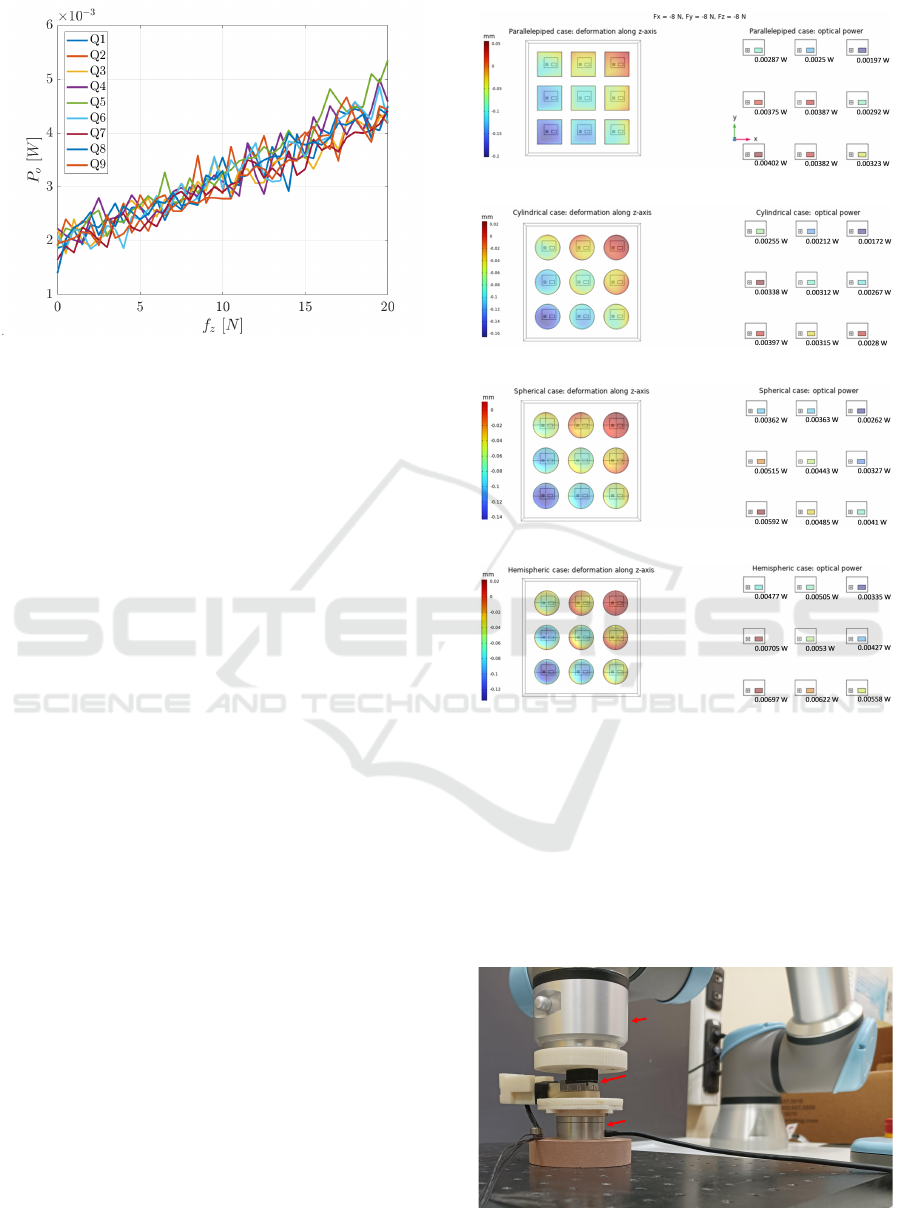
Figure 9: Optical powers with respect to the normal force
in the parallelepiped case.
for the spherical shape, 3.91e −4W/N in the hemi-
spheric geometry. Since the cylindrical case always
presents the lowest sensitivity, it has not been con-
sidered for the experimental comparison in the fol-
lowing section. Figure 10 allows additional observa-
tions about sensitivity, by showing how the taxel ma-
trix appears like a skew-symmetric matrix in terms of
mechanical displacement and optical power for some
simulation instants in presence of a tangential force
applied along the pad secondary diagonal. It is evi-
dent how the taxels 3 and 7 present the greater differ-
ence in values, the taxels 4 and 8 with respect to taxels
2 and 6 present a medium difference and the taxels on
the main diagonal are almost similar. This demon-
strates the relations among the force components, the
mechanical displacements and the optical power mea-
sured by photo-transistors. The matrix symmetry is
strictly related to force directions.
3 EXPERIMENTAL
EVALUATIONS
By considering the complexity of the deformable pad
both in terms of mechanical and optical features, also
an experimental evaluation of taxel performance has
been carried out. A suitable setup has been pre-
pared to evaluate some properties for the taxel: linear-
ity, sensitivity, hysteresis and repeatability. Linearity
and sensitivity are of paramount importance in sensor
characterization, but also hysteresis and repeatability
are computed. To obtain a complete sensor character-
ization, in this section experiments by applying only
normal forces and both normal and tangential com-
ponents have been considered. The setup is shown
in Fig. 11 and its main components are: a Robotous
(a)
(b)
(c)
(d)
Figure 10: Deformations along z−axis (left) and optical
powers (right), with a tangential force equal to −8N along
the secondary diagonal of taxel matrix: (a) parallelepiped
case, (b) cylindrical case, (c) spherical case, (d) hemispheric
case.
RFT40-SA01-D 6−axes force/torque sensor (used as
reference sensor), a 6 ×2 tactile sensor (equipped
with 3 pads with different taxel geometries) and an
UR5e robot manipulator (to apply external loads).
UR5e
tactile sensor
reference sensor
Figure 11: Experimental setup.
ICINCO 2023 - 20th International Conference on Informatics in Control, Automation and Robotics
106

For the experiments, a sensor with a matrix 6 ×2
has been used since the printed circuit board with op-
tical components was already available in the labora-
tory (see Fig. 12 for taxel numbering). This choice
does not limit the analysis in terms of linearity, sensi-
tivity, hysteresis and repeatability.
Figure 12: Taxel numbering used in the experiments.
The UR5e cobot is directly programmed by us-
ing its Graphical User Interface (GUI) available from
the teach pendant. It is used to apply the same force
components on the 3 different pads prepared with
the 3 different taxel shapes selected on the basis of
simulations (e.g., parallelepiped, spherical and hemi-
spheric). Figure 13 reports pictures of deformable
pads realized with silicone molding technique and
used in the experiments.
3.1 Sensor Characterization
As for simulations, two kinds of experiments have
been carried out in order to compare the tactile sen-
sor characteristics with respect to taxel shapes: the
first by applying only normal force in order to evalu-
ate the sensor along the z axis and the second by ap-
plying also tangential components for the evaluation
along the x and y axes. In the first experiment, the
robot is initially positioned almost in contact with the
pad, and then it is vertically moved of 1.1 mm along
z axis in 50 s (by resulting a velocity of 0.022 mm/s)
in order to apply a normal force to the pad. During
the linear movement in the operative space the robot
applies a normal force from 0 N to 10 N with a veloc-
ity of 0.2 N/s. Figure 14 reports the normal force f
z
signal from the reference sensor and the taxel voltage
variations ∆v
i
acquired during the experiment for the
parallelepiped case. From these data the sensitivity
(a) (b) (c)
Figure 13: Pad with different taxel geometries: paral-
lelepiped case (a), spherical case (b), and hemispheric case
(c).
for each taxel can be evaluated as the mean slope of
the force-voltage relation. It appears different for the
12 taxels, by varying from a minimum of 0.0196 V/N
achieved by the taxel 3 to a maximum of 0.0355 V/N
reached by the taxel 11. The taxel with maximum sen-
sitivity has been used to evaluate the other features,
since it corresponds to the worst case. In particular,
the hysteresis error has been evaluated as
e
h
=
|
∆v
incr
−∆v
decr
|
v
max
·100 (5)
where ∆v
incr
and ∆v
decr
are the voltage variations cor-
responding to two consecutive time ranges when the
force, in Fig. 14, increases and decreases respectively,
while v
max
is the maximum ∆v
i
value reached during
the experiment. Similarly, the repeatability error has
been evaluated as
e
r
=
|
∆v
a
−∆v
b
|
v
max
·100 (6)
where ∆v
a
and ∆v
b
are the voltage variations cor-
responding to the two time ranges when the force,
in Fig. 14, increases (or decreases). For the paral-
lelepiped case the hysteresis error is e
h
= 1.88% and
the repeatability error is e
r
= 2.08% for the taxel 11.
Figure 15 reports the graphs used for e
h
and e
r
com-
putation. For the spherical geometry, the same ac-
quired data are reported in Fig. 16. The minimum
sensitivity is 0.00467 V/N, reached by the taxel 10,
while the maximum one is 0.00716 V/N, achieved
by the taxel 11. Figure 17 reports data of taxel 11
for hysteresis and repeatability, and the computed er-
rors are e
h
= 6.87% and e
r
= 1.33%, respectively.
Finally, for the hemispheric shape the data are re-
ported in Fig. 18. The sensitivity ranges from a min-
imum of 0.00335 V/N for the taxel 1 to a maximum
of 0.00869 V/N for the taxel 8. As for previous case,
Fig. 19 reports data related to the taxel with the max-
imum sensitivity (taxel 8 for this shape) in order to
Figure 14: Parallelepiped case: (top) normal force applied
and (bottom) taxel voltage variations.
Multiphysics Simulation for the Optimization of an Optoelectronic-Based Tactile Sensor
107
Figure 15: Parallelepiped case: (left) data for hysteresis er-
ror and (right) data for repeatability error.
evaluate the hysteresis error e
h
= 10.3% and the re-
peatability error e
r
= 3.35%. The main important
feature highlighted from these experimental data with
respect to simulation data is the nonlinearity in the
force-voltage relations. In particular, while the paral-
lelepiped case is almost linear (see Fig. 15), the spher-
ical case shows a non negligible nonlinearity (see
Fig. 17) and the hemispheric case a high nonlinear-
ity (see Fig. 19). By evaluating the nonlinearity error
as
e
nl
=
|
∆v
incr
−∆v
nom
|
v
max
·100, (7)
where ∆v
incr
is the voltage variations corresponding
to the first time range when the force increases, and
∆v
nom
is the voltage variations corresponding to ideal
linear case, the following values are obtained: e
nl
=
3.18% for the parallelepiped case, e
nl
= 5.38% for the
spherical case, and e
nl
= 11.7% for the hemispheric
one. Thus, the performance in terms of linearity are
clearly better for the parallelepiped case.
The comparison of characteristics along the x and
the y axes also has been carried out. In order to re-
produce simulated case, the robot, initially positioned
almost in contact with the pad, is vertically moved of
1.1mm along z axis in 50 s, by reaching a constant
normal force of about 10N. Then, the robot is moved
of 1 mm along x−axis and 1 mm along y−axis simul-
Figure 16: Spherical case: (top) normal force applied and
(bottom) taxel voltage variations.
Figure 17: Spherical case: (left) data for hysteresis error
and (right) data for repeatability error.
Figure 18: Hemispheric case: (top) normal force applied
and (bottom) taxel voltage variations.
taneously, by obtaining a diagonal tangential force.
Also in this case the velocity is 0.022mm/s and the
trajectory is executed forward and backward, in or-
der to obtain an increasing and decreasing phase for
the tangential force. The sensitivity with respect to
tangential force components have been evaluated on
the same taxels selected from the normal case (i.e.,
the ones with the maximum sensitivity with respect to
normal force). For the parallelepiped case, the taxel
11 presents a sensitivity along the x−axis equal to
0.0342V/N and along the y−axis equal to 0.0314V/N
(see Fig. 20). For the spherical geometry, the taxel 11
reaches a sensitivity of 0.00271V/N along the x−axis
and 0.00276 V/N along the y−axis (see Fig. 21). At
last, for the hemispheric case the taxel 8 presents a
sensitivity of 0.00668V/N along the x−axis and of
0.00569V/N along the y−axis (see Fig. 22).
Figure 19: Hemispheric case: (left) data for hysteresis error
and (right) data for repeatability error.
ICINCO 2023 - 20th International Conference on Informatics in Control, Automation and Robotics
108

Figure 20: Parallelepiped case: voltage variations with re-
spect to tangential force components.
3.2 Comparison and Discussion
In order to compare simulation and experimental data
among the different shapes for the reflective cells,
the main important data have been summarized and
discussed in this section. First of all, the sensitiv-
ity with respect to both normal and tangential com-
ponents (see Tab. 1), estimated from simulation data,
show that the cylindrical shape presents the lower val-
ues (particularly for the tangential case) and hence
the experimental case has not been implemented to
reduce the case studies. Among the other cases the
sensitivity is almost of the same order. Obviously,
in simulation all taxels of the same shape present
the same features. Instead, by considering the ex-
perimental data, the taxel responses are different due
to realization processes of electronic and mechani-
cal components, hence it could be interesting to eval-
uate the minimum and maximum sensitivities. Ta-
ble 2 summarizes these sensitivities for the differ-
ent shapes. The absolute values cannot be directly
compared with simulated results, since the units are
different, but both cases (minimum and maximum)
show similar sensitivity for spherical and hemispher-
ical cases, while parallelepiped case is more sensitive
up to one order of magnitude. This difference with
Figure 21: Spherical case: voltage variations with respect
to tangential force components.
Figure 22: Hemispheric case: voltage variations with re-
spect to tangential force components.
simulation case probably depends on the mechanical
realization trough silicone moulds technique of pads
by means of 3D printed moulds: the flat surface (in
parallelepiped case) can be perfectly realized, while
the spherical and hemispherical shapes are locally ap-
proximated with small discrete steps by the 3D print
technology. The sensitivities experimentally evalu-
ated with respect to tangential components, and re-
ported in Tab. 3, confirm the same observations done
for normal force: the parallelepiped case shows a sen-
sitivity higher of one order of magnitude. Finally, the
main feature highlighted from the experiments is the
nonlinearity shown by the different shapes. As sum-
marized in Tab. 4, the spherical case presents a nonlin-
earity almost double with respect to the parallelepiped
case and the hemispheric case almost four times more.
As a consequence the parallelepiped case appears as
the best choice by considering its features also with
respect to current manufacturing processes.
Table 1: Simulations: sensitivity to normal and tangential
forces with respect to taxel shapes.
Normal[W/N] Tangential[W/N]
Parallelepiped 1.48e-4 2.48e-4
Cylindrical 1.11e-4 1.87e-4
Spherical 1.4e-4 2.66e-4
Hemispheric 2.48e-4 3.91e-4
Table 2: Experiments: minimum and maximum sensitivity
to normal force with respect to taxel shapes.
Min [V/N] Max [V/N]
Parallelepiped 0.0196 0.0355
Spherical 0.00467 0.00716
Hemispheric 0.00335 0.00869
4 CONCLUSIONS
This paper reported the steps followed for the real-
ization of the models of the two main parts compos-
Multiphysics Simulation for the Optimization of an Optoelectronic-Based Tactile Sensor
109
Table 3: Experiments: sensitivity to tangential force with
respect to taxel shapes.
along x [V/N] along y [V/N]
Parallelepiped 0.0342 0.0314
Spherical 0.00271 0.00276
Hemispheric 0.00668 0.00569
Table 4: Experiments: nonlinearity with respect to taxel
shapes.
Nonlinearity e
nl
[%]
Parallelepiped 3.18
Spherical 5.38
Hemispheric 11.7
ing the considered optoelectronic-based tactile sen-
sor: the photoreflector and the deformable layer. The
simulation has been used to determine how differ-
ent shapes of the reflective cells influence the per-
formance of the sensor. In particular, four different
shapes have been considered: parallelepiped, cylin-
drical, spherical, and hemispheric. Some tests have
been carried out to check the response of the simu-
lated model to different stimuli. Then, similar tests
have been repeated in a real setup in order to compare
the evaluated taxel shapes. Data from both the simu-
lation results and the measurements from the real sen-
sor have been used to discuss the best choice for the
taxel shape, also by considering the limitations due
to manufacturing processes. The results for proper-
ties such as linearity and sensitivity show differences
between simulations and experiments probably due
to the following reasons: in the simulation, the con-
sidered walls are completely reflective or absorbent,
while the real pads have white and black walls that are
not totally reflective or absorbent; the molds used for
realizing the silicone pads, being 3D printed, present
imperfections (i.e., grooves, small steps) that make
the actual walls not smooth, differently from those
in the simulation model, particularly for hemispheric
and spherical cases. The consequence of this lack of
smoothness is that, in the real case, the ray reflections
are locally quite different from the simulated case.
Future studies will be devoted to enhancing the sim-
ulation model by taking into account the aforemen-
tioned imperfections, e.g., by modifying the mechani-
cal model of the deformable layer taking into account
the non-smooth surfaces due to the production pro-
cess, or by investigating the possibility to consider
different reflection modalities in the ray tracing tech-
nique.
ACKNOWLEDGMENTS
This work was partially supported by the European
Commission under the Horizon Europe research grant
INTELLIMAN, project ID: 101070136
REFERENCES
Alqurashi, M. M., Ganash, E. A., and Altuwirqi, R. M.
(2022). Simulation of a low concentrator photovoltaic
system using comsol. Applied Sciences, 12(7).
Amiri, P., Casals, O., Maur, M. A. d., and Prades, J. (2022).
Ray tracing simulation of a gan-based integrated led-
photodetector system. In 2022 Int. Conf. on Numeri-
cal Simulation of Optoelectronic Devices (NUSOD).
Cirillo, A., Cirillo, P., De Maria, G., Natale, C., and Pirozzi,
S. (2014). A FE analysis of a silicone deformable in-
terface for distributed force sensors. AIP Conference
Proceedings, 1599(1):485–488.
Cirillo, A., Costanzo, M., Laudante, G., and Pirozzi, S.
(2021). Tactile sensors for parallel grippers: Design
and characterization. Sensors, 21(5).
Ferreira, G. M., Silva, V., Minas, G., and Catarino, S. O.
(2022). Simulation study of vertical p-n junction pho-
todiodes’ optical performance according to cmos tech-
nology. Applied Sciences, 12(5).
Khamis, H., Xia, B., and Redmond, S. J. (2019). A novel
optical 3d force and displacement sensor – towards in-
strumenting the papillarray tactile sensor. Sensors and
Actuators A: Physical, 291:174–187.
Lu, Z., Gao, X., and Yu, H. (2022). Gtac: A
biomimetic tactile sensor with skin-like heteroge-
neous force feedback for robots. IEEE Sensors Jour-
nal, 22(14):14491–14500.
NJL5908AR Datasheet (2015). NJL5908AR Datasheet
Ver.2015-02-17. New Japan Radio Co. LTD, Tokyo,
Japan.
Wang, S., She, Y., Romero, B., and Adelson, E. (2021).
Gelsight wedge: Measuring high-resolution 3d con-
tact geometry with a compact robot finger. In 2021
IEEE Int. Conf. on Robotics and Automation (ICRA).
Ward-Cherrier, B., Pestell, N., Cramphorn, L., Winstone,
B., Giannaccini, M. E., Rossiter, J., and Lepora, N. F.
(2018). The tactip family: Soft optical tactile sen-
sors with 3d-printed biomimetic morphologies. Soft
Robotics, 5(2):216–227.
ICINCO 2023 - 20th International Conference on Informatics in Control, Automation and Robotics
110
