
Ultra-Wideband Direct RF Sampling Transceiver Design
Ahcene Bellabas
1 a
, Ammar Mesloub
1 b
, Belaid Ghezali
2
, Abdelmadjid Maali
3 c
and Tahar Ziani
3
1
Lab. Traitement du Signal, Ecole Militaire Polytechnique, BP 17 Bordj El Bahri, Algeria
2
Ecole Sup
´
erieure ALI CHABATI, Algiers, Algeria
3
Lab. Syst
`
emes
´
Electroniques et Num
´
eriques, Ecole Militaire Polytechnique, BP 17 Bordj El Bahri, Algeria
Keywords:
Direct RF Sampling, Radio Transceiver, Radar, UWB, FPGA, ADC, DAC.
Abstract:
This paper focuses on the design and development of a direct RF sampling transceiver for ultra-wideband
(UWB) radar applications. By directly synthesizing and capturing the desired signal, direct RF sampling
simplifies the system and reduces analog components. It overcomes the limitations of heterodyne transceiver
architecture, particularly the presence of harmonics and spurious signals at the mixer output. This approach
enables digital processing and offers flexibility for system reconfiguration. Advanced techniques and concepts
in radio transceiver design methodology are explored, discussing the constraints involved in meeting system
design requirements for optimal radar system performance. A design of a direct RF sampling transceiver ar-
chitecture for given requirements set is proposed, which includes concise frequency planning, digital receiver
design, and a direct RF waveform synthesis scheme. Furthermore, experimental results demonstrate the suit-
ability of the proposed direct RF sampling transceiver for UWB radar applications.
1 INTRODUCTION
UWB radar has attracted significant attention in both
military and civilian fields, particularly in the do-
mains of target detection, imaging, and recognition
(Li et al., 2020). It offers several advantages, in-
cluding high range resolution, robust penetration, low
power consumption, and strong anti-interference ca-
pabilities. These attributes make UWB radar highly
valuable in applications such as precision radar imag-
ing for see-through-the-wall technology, monitoring
vital signs of the human body, and precise localization
using time-of-arrival techniques (Taylor, 2020; Lim
et al., 2019).
The UWB transceiver is the crucial component in
UWB radar systems, enabling the transmission and
reception of signals across a wide frequency range,
enhancing system performance (Fang et al., 2022;
Wang et al., 2021). Figure 1 illustrates a typical block
diagram of a UWB radar transceiver, including both
the transmitter and receiver sections. The transmit-
ter section includes essential components such as a
waveform generator, mixer, power amplifier, and an
antenna. These elements work in conjunction to gen-
a
https://orcid.org/0000-0002-2375-5364
b
https://orcid.org/0000-0002-3754-8382
c
https://orcid.org/0000-0003-3652-1943
erate and transmit the UWB radar signals. The re-
ceiver section consists of an antenna, a low noise am-
plifier, a mixer, a band-pass filter, and a demodulator.
These components are responsible for capturing and
processing the incoming UWB radar signals, allow-
ing for signal detection and further analysis.
Figure 1: A typical block diagram of a UWB radar
transceiver.
To meet the increasing performance requirements,
improve flexibility, and reduce design time of radio-
frequency (RF) UWB transceivers, it is advanta-
geous to develop a design that supports multiple fre-
quency bands, various standards, and diverse appli-
cations (Khatri and Mishra, 2022; Saoudi and Ghar-
iani, 2021; Johannsen et al., 2020). Therefore, the
functionality is being migrated from analog hardware
to Hardware Description Language (HDL) functions,
which will be implemented on suitable digital hard-
ware. This approach provides enhanced flexibility,
Bellabas, A., Mesloub, A., Ghezali, B., Maali, A. and Ziani, T.
Ultra-Wideband Direct RF Sampling Transceiver Design.
DOI: 10.5220/0012175800003543
In Proceedings of the 20th International Conference on Informatics in Control, Automation and Robotics (ICINCO 2023) - Volume 2, pages 111-118
ISBN: 978-989-758-670-5; ISSN: 2184-2809
Copyright © 2023 by SCITEPRESS – Science and Technology Publications, Lda. Under CC license (CC BY-NC-ND 4.0)
111

enabling the transceiver to be digitally configured to
meet the current specifications, taking advantage of
the availability of high-performance analog-to-digital
converters (ADCs) and digital-to-analog converters
(DACs). Several researches have been conducted on
this framework, taking advantages of direct RF sam-
pling solutions to achieve digital functions on radar
systems (Furuichi et al., 2019; Siafarikas and Volakis,
2018; Haberl et al., 2017). However, as functionality
is moved from analogue hardware to HDL functions
on digital hardware, the ADC and DAC performance
requirements increase drastically.
In this paper, a design and development of a di-
rect RF sampling transceiver for UWB radar appli-
cations has been considered. We explore and dis-
cuss advanced techniques and concepts of the radio
transceiver’s design methodology to meet design re-
quirements and achieve radar system performances.
The main contributions of this paper can be sum-
marized as follows:
• A concise frequency planning for both the direct
RF waveform synthesis and direct RF sampling
schemes in the UWB transceiver design, for a
given design requirements;
• Hardware architecture design for the UWB
transceiver including cascade analysis for the ana-
log front-end part;
• Hardware implementation using digital logic for
a compact RF generation and data capture system
using high-speed data converters.
These contributions provide valuable insights and
practical solutions for the design and implementation
of UWB transceivers.
The reminder of this paper is organized as follows:
Section 2 provides a summary of the main functions
and design requirements set for the design and de-
velopment of a UWB direct RF sampling transceiver.
Section 3 presents the frequency plan that has been
developed to optimize the performance of the system.
It explains the approach taken to achieve optimal fre-
quency utilization and minimize interference. Section
4 introduces the architecture of the UWB transceiver
based on direct RF sampling. Section 5 focuses on the
crucial parameters of the ADC and DAC in the direct
RF sampling radar receiver and transmitter, respec-
tively. Section 6 provides a detailed explanation of
the various calculations and analyses conducted dur-
ing the design process. Section 7 presents the hard-
ware implementation of the signal generation and data
capture components of the proposed UWB transceiver
architecture, utilizing an FPGA board. Finally, con-
clusions are drawn in section 8.
2 MAIN FUNCTIONS AND
DESIGN REQUIREMENTS
The transceiver is mainly used to generate the radar
excitation signal, process the received echo signals,
and converts the RF analog echoes into digital sig-
nals at the baseband (Mohammadi and Ghannouchi,
2012). Its main functions, based on the system design
requirements, include:
• Processing the low-power echo signal from
the antenna into baseband digital In-phase and
Quadrature (IQ) signals. This involves filtering,
amplification, frequency conversion, A/D sam-
pling, and digital demodulation (DDC: Digital
Down Conversion);
• Transmitting the echo data (baseband digital IQ),
timing signals, and control instructions to the
radar signal processing system;
• Generating the required excitation signals at the
radar’s operating frequency with the appropriate
waveform to meet the specific radar application
requirements.
Depending on the requirements of the radar applica-
tion, we have to design the UWB direct RF sampling
transceiver architecture as a real-time processing sys-
tem with high dynamic range, low noise, and good
harmonics and Spurs Rejection. Key system design
requirements set are summarized in Table 1.
Table 1: Design Requirements.
Parameter Value
Operating frequency range [3.1-3.8] GHz
Signal bandwidth 700 MHz
Transmitting output power ≥ 7 dBm
Noise figure ≤ 10 dB
Dynamic range ≥ 80 dB
A/D resolution ≥ 14 Bits
Harmonics/Spurs rejection ≥ 55 dB
3 DRAWING UP THE
FREQUENCY PLAN
System designers are moving toward direct RF sam-
pling to reduce system size and power by removing an
entire down-conversion stage. In this case, the instan-
taneous bandwidth B can be smaller than the ADC’s
Nyquist zone and frequency planning can help to op-
timize system performance (Siafarikas and Volakis,
2020).
We begin by selecting the appropriate sampling
frequency for the receiver section of the transceiver.
ICINCO 2023 - 20th International Conference on Informatics in Control, Automation and Robotics
112
Drawing up a frequency plan for a direct RF sam-
pling receiver consists mainly on choosing the ade-
quate ADC sampling rate (F
S
). The RF sub-sampling
architecture utilizes the band-pass sampling theorem,
as described in (Shawn R. German, 2020). By apply-
ing equations (1) and (2), we set up a table of possible
sampling frequencies for the proposed direct RF sam-
pling receiving scheme (Table 2).
2
F
H
N
≤ F
S
≤ 2
F
L
N − 1
(1)
2 ≤ N ≤
F
H
F
H
− F
L
(2)
where F
H
= 3.8 GHz, F
L
= 3.1 GHz and N is the
Nyquist zone index. In Table 2, F
Smin
=
2F
H
N
and
F
Smax
=
2F
L
(n−1)
.
Table 2: Possible sampling frequencies
N F
Smin
(MHz) F
Smax
(MHz)
2 3800 6200
3 2522 3100
4 1900 2066
5 1520 1550
According to equation (2), there are four (04)
available zones for selecting the appropriate sampling
frequency from the range [F
Smin
− F
Smax
] defined in
the above table. Several key design considerations
need to be taken into account, including design fea-
sibility, availability of ADC products in the market,
ADC performance, and analysis of frequency plan
charts for different sampling frequencies. In this case,
we have chosen a sampling rate of 2.6 Gsps for the
receiving part, which corresponds to the RF operating
band located in the 3
rd
Nyquist zone (N=3). This en-
sures that the band of interest is folded into the first
Nyquist zone [0,
F
S
2
], and the half sampling rate is
higher than the operating band (
F
S
2
> B = 700 MHz).
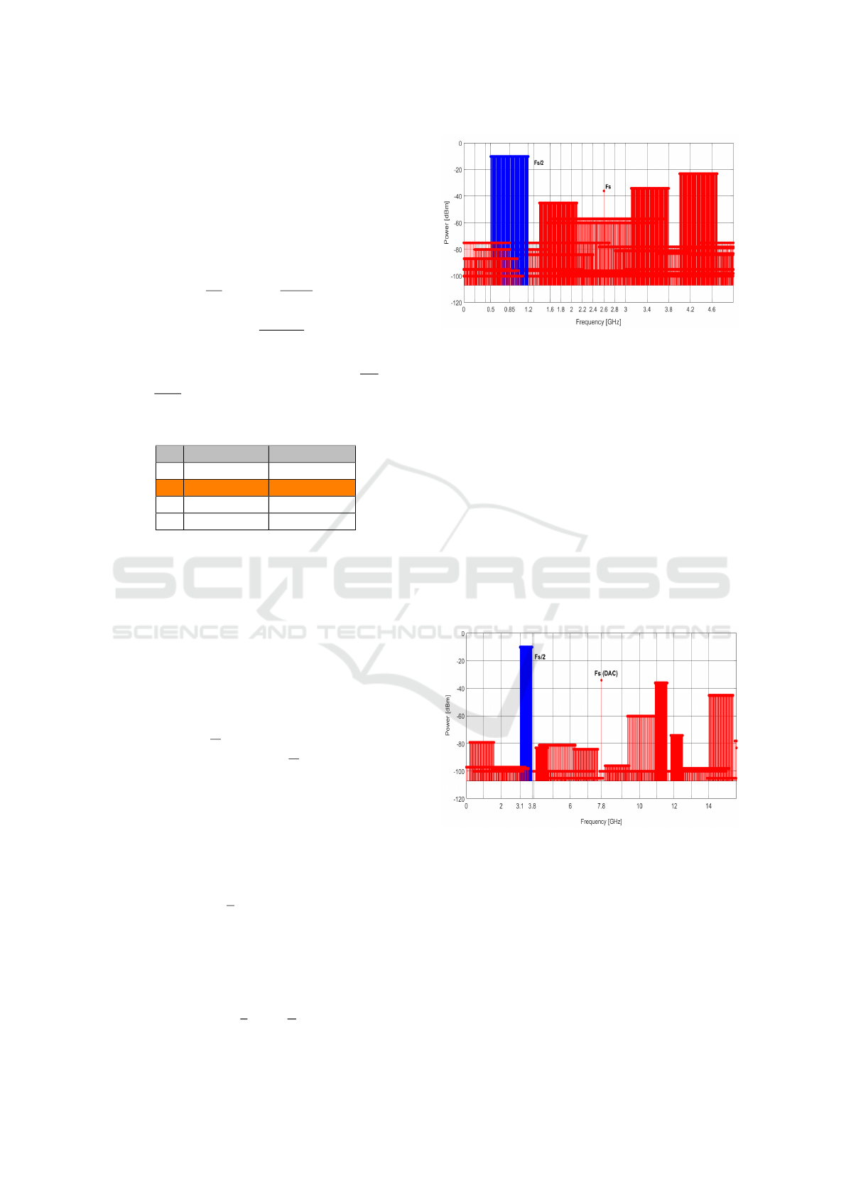
Figure 2 demonstrates that the frequency plan setup
results in a clean spectrum, ensuring more than 70 dB
overlapping harmonics and spurs rejection within the
desired signal bandwidth. The required instantaneous
bandwidth, B = 700 MHz, can be easily achieved us-
ing this frequency plan.
For the transmitting part of the transceiver, the op-
timal solution for selecting the sampling rate for the
DAC is to choose an
n
m
multiple of 2.6 GHz, where n
and m are positive integers. In this case, we consider
F
S
= 7.8 GHz, taking into account various design con-
siderations. It is important to ensure that the follow-
ing condition, expressed in equation (3), is satisfied
(Symons, 2013)
F
S
≥
5
2
(F
H
+
B
2
) (3)
Figure 2: Frequency plan chart for A/D conversion on re-
ceiving at @2.6 Gsps sampling rate.
Figure 3 shows that the frequency plan set-up, for
the transmitting part, leads clean spectrum, ensuring
more than 70 dB overlapping harmonics and spurs re-
jection within the desired signal bandwidth.
For the receiving scheme, the chosen frequency
plan involves down-converting the RF band [3.1-3.8]
GHz to the [0.5-1.2] GHz band through analog-to-
digital conversion using an ADC. Then, the instan-
taneous band is further down-converted to the base-
band using the DDC. For the transmitting scheme, the
direct RF sampling synthesis process is achieved by
up-converting the base-band signal bandwidth to the
RF band [3.1-3.8] GHz using the Quadrature Digital
Up-Converter (QDUC) process and D/A conversion
through a high sample rate DAC.
Figure 3: Frequency plan chart for UWB waveform gener-
ation @7.8 Gsps sampling rate.
4 HARDWARE ARCHITECTURE
In traditional signal waveform transmission, a homo-
dyne or superheterodyne architecture, involving mix-
ing and filtering stages, has been utilized to shift
the signal from the baseband to the RF center fre-
quency (R
¨
ojsel, 2013). However, by employing an
RF DAC, as depicted in Figure 4, the frequency trans-
Ultra-Wideband Direct RF Sampling Transceiver Design
113

lation functions of the signal chain are moved to the
digital domain. This eliminates the need for mixers,
IF filters, and Local Oscillators (LO) in the analog
signal chain, enabling direct synthesis at the working
frequency band.
The DAC operates at a conversion rate of 7.8
Gsps, ensuring that the output signal falls within the
first Nyquist zone of the DAC and avoids harmonic
distortion (Chuang et al., 2022). This placement al-
lows sufficient separation between transceiver’s fre-
quency band and the second Nyquist image band. The
relaxed frequency planning is made possible by the
frequency multiplying Phase-Locked Loop (PLL) in-
tegrated within the RF DAC, which generates the re-
quired 7.8 Gsps conversion rate. As a result, the DAC
output is directly within the [3.1-3.8] GHz frequency
band.
As shown in Figure 4, the excitation signal gener-
ation chain consists of a DAC, two Band Pass Filter
(BPF), a Low Pass Filter (LPF), and two amplifiers.
The amplifiers are configured to achieve the minimum
required signal output power of the transceiver, while
the LPF is used to attenuate the high-order harmonics
generated by the amplifiers.
Figure 4: Direct RF Sampling based transceiver architec-
ture.
In the designed receiving path, the RF signal is
directly digitized by the ADC and sent to the FPGA
for processing. The chosen ADC includes Digital
Down Conversion (DDC) for post-processing. This
approach simplifies the hardware design, making it
more flexible and cost-effective. Using digital hard-
ware avoids IQ amplitude and phase imbalance prob-
lems, which can generate unwanted image and DC
signals (Siafarikas and Volakis, 2020; Shawn R. Ger-
man, 2020; Li, 2014).
The receiving part consists of two RF amplifiers,
an attenuator for Sensitivity Time Control (STC), a
BPF, a transformer, two attenuators and an RF ADC
device. The amplifiers’ gain is adjusted to meet the
receiver system’s high dynamic range requirements
and maximize the linear dynamic range of the ADC
input (Texas-Instruments, 2017). The BPF is a filter
with 700 MHz bandwidth, effectively removing out-
of-band noise. The overall hardware design is char-
acterized by simplicity, low PCB layout complexity,
and lower design cost (Lewis et al., 2019). The two
attenuators are placed before the input of the ADC
to reduce overall gain and enhance return loss. The
transformer facilitate single-ended to differential con-
version with proper differential balance and ensure
impedance matching between the 50 Ω characteristic
impedance and the 100 Ω differential input resistance
of the ADC. The second amplifier is a linear amplifier
with increased drive capability to directly drive the
ADC device, thereby improving the total noise figure.
This approach is commonly employed to mitigate the
impact of high noise figure in the ADC (Kester, 2014).
The LPF, placed after the amplifier, serves to elimi-
nate high-power harmonics introduced by the ampli-
fiers before the A/D process. Note that the Single Pole
Double Throw (SP2T) switch is introduced to make
some common components for both transmitting and
receiving modes.
The hardware architecture of the designed RF
sampling transceiver is based on an FPGA device.
Thus, several crucial functions will be implemented
and executed within the FPGA. The key HDL-based
functions are as follows:
1. Waveform Generation Process
This function primarily involves the utilization of
a DAC device, which is controlled and configured
in real-time using HDL-based functions. These
functions include:
• Waveform library definition function;
• Generation of DAC patterns and configuration
using the JESD204B-TX interface;
• Generation of timing and synchronization sig-
nals for the specific radar application.
2. ADC Data Capture
The FPGA device captures the digital data from
the ADC for further digital processing. The se-
lected ADC utilizes the JESD204B-RX interface,
which needs precise configuration and HDL im-
plementation (Grace et al., 2021). Several param-
eters need to be carefully considered, including
the ADC sampling rate (F
S
), ADC resolution, IQ
signal bandwidth, and decimation factor.
ICINCO 2023 - 20th International Conference on Informatics in Control, Automation and Robotics
114

5 KEY COMPONENTS
SELECTION
The key component in the direct RF sampling receiv-
ing part is the ADC, which has a resolution of 14 bits
and a sampling rate of 2.6 Gsps. The selected ADC
is designed to support applications that involve direct
sampling of wide bandwidth analog signals up to 5
GHz. The key RF ADC parameters are:
• Resolution: 14 Bits;
• Sampling rate: 2.6 Gsps;
• 5 GHz analogue input full-scale power band-
width;
• SFDR (Spurious Free Dynamic Range): 70 dB (at
working frequency band);
• SNR (Signal to Noise Ratio): 60 dB (at working
frequency band);
• On-chip DDC: Offers more flexibility for FPGA-
based Data;
• JESD204B-based high-speed serialized output.
The key component in the direct RF sampling
transmitting part is the DAC, which has a resolution
of 14 bits, and a sampling rate of 9 Gsps. The selected
RF DAC converter offers key parameters that make it
suitable for applications involving direct sampling of
digital waveform synthesis up to 4.5 GHz. The fol-
lowing are the factors that influenced the selection of
this particular converter:
• Resolution: 14 Bits;
• Sampling Rate: 9 Gsps;
• Includes RF Sampling Direct Digital Synthesis
(DDS);
• Utilizes JESD204B-based high-speed configura-
tion interface, resulting in low PCB layout com-
plexity and enabling high sampling rate and wide-
band pattern generation;
• Supports both DDS and DUC operations.
6 DESIGN ANALYSIS
RF transceiver system designers are experiencing a
shift from the commonly used heterodyne architec-
ture to a direct RF-sampling approach (Siafarikas and
Volakis, 2020). In traditional receivers, the selection
of the ADC is based on key specifications such as
SNR and spurious-free dynamic range (SFDR). How-
ever, in direct RF-sampling receiveing part, designers
prioritize the impact of the RF ADC on the receiver
system’s noise figure (NF) instead (Kester, 2014).
6.1 Transmitting Power Gain and
Excitation Power
The analysis of the transmitting path gain cascade be-
gins at the output of the DAC, where the power is
measured to be -4 dBm. However, the system design
requirements specify that the excitation signal should
not be lower than P
min
= 7 dBm. Therefore, an over-
all cascade gain of 11 dB is necessary to achieve the
desired output power of 7 dBm at the end of the trans-
mitting path in the transceiver. Figure 5 illustrates
the final design and provides a distribution of the gain
along the transmitting path.
Figure 5: Lineup analysis for transmitting path gain and
excitation signal power.
6.2 ADC Noise Figure
In this section, we calculate the noise figure of the
ADC by using equation 4, similar to the approach em-
ployed in the RF sampling receiver study conducted
by (Shawn R. German, 2020).
F =
SNR
in
SNR
out
=
S
I
N
I
GS
I
(N
I
+N
A
)×G
= 1 +
N
A
N
I
(4)
where:
• N
I
represents the noise into the ADC, which is
equal to KT and has a value of −174 dBm/Hz.
Here, K is Boltzmann’s constant (1.3810
−23
J/K)
and T is the temperature (290 °K);
• N
A
refers to the ADC noise power and can be cal-
culated using the following equation
N
A
= P
max
− 1 − SNR
A
–10log
10
(
F
S
2
) dBm/Hz (5)
where, P
max
is the full-scale power into the ADC,
SNR
A
is the SNR of the ADC provided by ADC man-
ufacturers though.
Considering the selected 14-bit ADC with F
S
=
2.6 Gsps, an input impedance of R
in
= 100 Ω, an
SNR
A
of 60 dBc, a P
max
of 13 dBm, then:
Ultra-Wideband Direct RF Sampling Transceiver Design
115
N
A
= -139 dBm/Hz
To use equation 4, we need to convert the values
of N
I
and N
A
into their linear equivalents
F = 1 + 10
((−139+174)/10)
= 3163 (6)
Thus, the ADC noise figure is
NF = 10 log
10
(3163) = 35 dB. (7)
6.3 Receiver Noise Figure and Receiver
Gain
Using the Friis formula for the cascade of noise fig-
ure (Shawn R. German, 2020), the resulting receiver
noise figure is 8.82 dB (Figure 6), which satisfies the
design requirements of being less than 10 dB. The
specifications for this design aim for even lower noise
figures, preferably around 2 dB or less, for the com-
plete receiving path, from the antenna to the ADC,
including the RF front-end. Achieving such perfor-
mance is possible by carefully selecting the front-
end LNA positioned between the antenna and the de-
signed transceiver shown in Figure 4.
Figure 6: Lineup analysis for receiving path noise figure
and receiving gain.
Figure 6 shows the lineup of the receiving path
and provides an overview of the gain distribution. To
achieve a linear dynamic range of 55 dB and a full-
scale ADC power input of 13 dBm, a required gain of
35 dB is specified. This target gain of 35 dB can be
easily achieved by the configuration of the receiving
path lineup.
6.4 Dynamic Range
In this section, the dynamic range is calculated us-
ing the same approach conducted by (Wu, 2019). The
receiving path is required to have a dynamic range
greater than 80 dB, taking into account the STC func-
tion. For the selected ADC, operating at its maximum
sampling rate, the maximum allowable signal power
at the input is 13 dBm, ensuring SNR
A
of 60 dB. Thus,
the noise power is calculated as N
b
= 13 - 60 = -47 dB.
When designing for a 55 dB output dynamic, the min-
imum noise level at the ADC input is N
b min
= 13 - 55
= -42 dB, which is higher than -47 dB. Therefore, the
linear input dynamic of the ADC satisfies the require-
ment of a linear output dynamic greater than 55 dB.
Equation 8 provides the equivalent noise power at the
input of the receiving part, with NF of 8.82 dB
N
i
= −114 + 10 log
10
(700) + 8.82 = −77 dBm (8)
The gain of the receiving part is 35 dB. The maxi-
mum power at the input of the ADC is 13 dBm, ther-
fore the maximum power at the input of the receiving
path is
P
in max
= 13 − 35 = −22 dBm (9)
In addition, considering the maximum attenuation of
the STC function as 31 dB, the dynamic range of the
digital receiver can be calculated as follows
DR = −22 − (−77) + 31 = 86 dB (10)
This result meets the requirement on the dynamic
range of the receiving part, which must be greater than
80 dB.
7 HARDWARE
IMPLEMENTATION
The compact RF signal generation and data capture
system implemented on the FPGA, associated with
DAC and ADC, represents the core element of the
proposed transceiver architecture (Figure 4) by in-
tegrating it with the designed analog front-end dis-
cussed previously.
In this section, we present a hardware implemen-
tation of the signal generation and data capture part
of the proposed UWB transceiver architecture on an
FPGA board, utilizing a DAC to generate a UWB RF
signal within the frequency range of 3.1 to 3.8 GHz,
and an ADC to convert the generated RF signal back
to the digital domain, enabling further processing on
the same FPGA board (Figure 7). Finally, we will plot
the spectrum of the captured data for visualization and
analysis.
Using an FPGA’s programmable logic, we can im-
plement custom logic to generate the desired RF sig-
nal within [3.1-3.8] GHz frequency range. The FPGA
communicates with the DAC through high-speed se-
rial interface, to send digital samples representing the
RF waveform. For this application, a DAC with a 7.8
Gsps sampling rate is used to ensure accurate UWB
ICINCO 2023 - 20th International Conference on Informatics in Control, Automation and Robotics
116
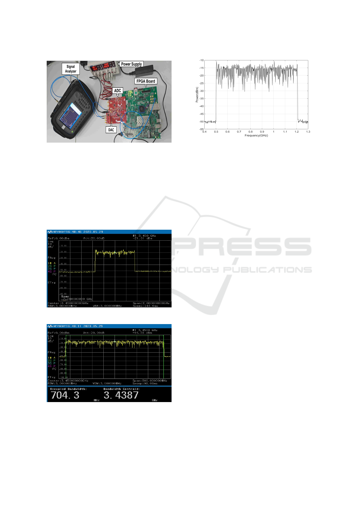
Figure 7: UWB direct RF sampling architecture for signal
generation and data capture.
RF signal generation. The implemented logic on the
FPGA provides the necessary configuration and con-
trol signals to the DAC, ensuring proper synchroniza-
tion.
The spectrum of the generated signal is depicted
in Figure 8 saved from a spectrum analyzer, and the
occupied bandwidth of the signal was measured to be
704 MHz using the same spectrum analyzer, as shown
in Figure 9.
Figure 8: Spectrum of the generated UWB RF signal.
Figure 9: Occupied bandwidth of the generated UWB RF
signal.
After generating the UWB RF signal, it can be
converted back into digital samples using the ADC,
Figure 10: Spectrum of the captured UWB RF signal data.
and captured on the FPGA board. The ADC receives
the analog RF signal, digitizes it by sampling at 2.6
Gsps, and forwards the captured data to the FPGA for
further processing. The ADC converts the RF signal
and preserve its characteristics during the conversion
process according to the design parameters discussed
above. The FPGA board configures and controls the
ADC, ensuring synchronization with the RF signal
generation and the accurate capture of the converted
data. These data are sent to the computer to plot the
spectrum presented on the Figure 10.
The RF signal generation and data capture sys-
tem implemented on the FPGA, associated with the
DAC and ADC, can have many practical applications
by combining it with a suitable RF analog front-end.
The integration of the FPGA, DAC, and ADC enables
the implementation of a powerful RF signal genera-
tion and capture system.
8 CONCLUSION
This paper presented a complete design and develop-
ment of a direct RF sampling transceiver for UWB
radar applications. Direct digitization in the RF do-
main overcomes issues related to DC offsets, im-
age signals, frequency-dependent components, and
sources of noise and errors, such as LO leakage and
IQ amplitude and phase imbalance. To do so, much
faster data converters, ADC and DAC, are required.
The paper provides a concise frequency planning
for both the direct RF waveform synthesis and direct
RF sampling schemes in the UWB transceiver de-
sign, meeting the given design requirements. This
frequency planning plays a crucial role in optimiz-
ing the system’s performance and minimizing inter-
ference. Furthermore, the hardware architecture of
the UWB direct RF sampling transceiver is designed,
incorporating cascade analysis for the analog front-
end part to optimize its performance. This analysis
Ultra-Wideband Direct RF Sampling Transceiver Design
117

enables us to carefully select and configure the com-
ponents in the receiving and transmitting paths, ensur-
ing efficient signal generation and accurate data cap-
ture. Moreover, the successful implementation of the
designed compact RF signal generation and data cap-
ture on an FPGA, using high-speed data converters,
showcases the practicality and feasibility of the pro-
posed design.
This work provides valuable insights and practi-
cal solutions for designing and implementing UWB
direct RF sampling transceivers, making it a valuable
resource for radar technology researchers and engi-
neers. Future research should focus on integrating
hardware implementation of the signal generation and
data capture part with the designed analog front-end
for testing and validating the design.
REFERENCES
Chuang, K., Yektaii, H., McLaurin, D., and Mayer, C.
(2022). Radio challenges, architectures, and design
considerations for wireless infrastructure: Creating
the core technologies that connect people around the
world. IEEE Microwave Magazine, 23(12):42–59.
Fang, Z., Wang, W., Wang, J., Liu, B., Tang, K., Lou, L.,
Heng, C.-H., Wang, C., and Zheng, Y. (2022). In-
tegrated wideband chip-scale rf transceivers for radar
sensing and uwb communications: A survey. IEEE
Circuits and Systems Magazine, 22(1):40–76.
Furuichi, T., Motoyoshi, M., Kameda, S., and Suematsu, N.
(2019). A study on direct rf undersampling receiver
configuration considering timing skew spurs using
time-interleaved adc. In 2018 Asia-Pacific Microwave
Conference, APMC 2018 - Proceedings, Asia-Pacific
Microwave Conference Proceedings, APMC, pages
1525–1527. Institute of Electrical and Electronics En-
gineers Inc.
Grace, C. R., Fong, E., Gnani, D., Stezelberger, T., and
Denes, P. (2021). A 24-channel digitizer with a
jesd204b-compliant serial interface for high-speed de-
tectors. IEEE Transactions on Nuclear Science,
68(4):426–433.
Haberl, M., Sanftl, B., Trautmann, M., Weigel, R., and
Koelpin, A. (2017). A direct rf-to-baseband quadra-
ture subsampling receiver using a low cost adc. In
2017 IEEE Radio and Wireless Symposium (RWS),
pages 144–146. IEEE.
Johannsen, N. L., Peitzmeier, N., Hoeher, P. A., and Man-
teuffel, D. (2020). On the feasibility of multi-mode
antennas in uwb and iot applications below 10 ghz.
IEEE Communications Magazine, 58(3):69–75.
Kester, W. (2014). Adc noise figure—an often misunder-
stood and misinterpreted specification. Analog De-
vices.
Khatri, R. and Mishra, D. (2022). Fully optimized ultra
wideband rf receive front end. Jordanian Journal of
Computers and Information Technology, 8(2).
Lewis, K., Taft, R., Bodem, A., Hoehn, T., Schmitz, P.,
Nair, V., Savic, F., Childs, M., Kramer, P., Sandner, J.,
and Guibord, M. (2019). Single event effects testing
for the adc12dj3200qml-sp 12-bit, dual 3.2-gsps sin-
gle 6.4-gsps, rf-sampling, jesd204b, analog-to-digital
converter (adc). In 2019 IEEE Radiation Effects Data
Workshop, pages 1–6.
Li, J., Zhang, Q., and Zheng, G. (2020). Research on ultra-
wideband radar target recognition method. In Jour-
nal of Physics: Conference Series, volume 1651, page
012194. IOP Publishing.
Li, Y. (2014). In-Phase and Quadrature Imbalance: Mod-
eling, Estimation, and Compensation. SpringerBriefs
in Electrical and Computer Engineering.
Lim, S., Lee, S., Jung, J., and Kim, S.-C. (2019). Detec-
tion and localization of people inside vehicle using
impulse radio ultra-wideband radar sensor. IEEE Sen-
sors Journal, 20(7):3892–3901.
Mohammadi, A. and Ghannouchi, F. M. (2012). RF
transceiver design for MIMO wireless communica-
tions, volume 145. Springer Science & Business Me-
dia.
R
¨
ojsel, P. (2013). Rf mems-based wireless architectures and
front-ends. In Handbook of Mems for Wireless and
Mobile Applications, pages 207–224. Elsevier.
Saoudi, H. and Ghariani, H. (2021). A digitally con-
trolled multichannel spectrally efficient low-power
transceiver for ultra-wideband cognitive radio appli-
cations. Journal of Circuits, Systems and Computers,
30(12):2150208.
Shawn R. German, O. B. (2020). Basic radar analysis.
Siafarikas, D. and Volakis, J. L. (2018). Direction find-
ing of ultra-wideband signals using direct rf sampling.
In 2018 IEEE International Symposium on Antennas
and Propagation, USNC/URSI National Radio Sci-
ence Meeting, pages 1789–1790. IEEE.
Siafarikas, D. and Volakis, J. L. (2020). Toward direct rf
sampling: Implications for digital communications.
IEEE Microwave Magazine, 21(9):43–52.
Symons, P. (2013). Digital waveform generation. Cam-
bridge University Press.
Taylor, J. D. (2020). Ultra-wideband radar overview. In
Introduction to ultra-wideband radar systems, pages
1–10. CRC Press.
Texas-Instruments (May 2017). Direct rf-sampling radar
receiver for l-, s-, c- and x-band using adc12dj3200
reference design.
Wang, B., Song, H., Rhee, W., and Wang, Z. (2021).
Overview of ultra-wideband transceivers—system ar-
chitectures and applications. Tsinghua Science and
Technology, 27(3):481–494.
Wu, J. (2019). Advanced Metric Wave Radar. Springer.
ICINCO 2023 - 20th International Conference on Informatics in Control, Automation and Robotics
118
