
Meta-Heuristic Optimization of Transistor Sizing in
CMOS Digital Designs
Prashanth H C
a
and Madhav Rao
b
International Institute of Information Technology Bangalore, India
Keywords:
Circuit Optimization, EDA, Single Objective Functions, Multi-Objective Functions, VLSI, Adder Design.
Abstract:
Designing new custom standard cells or digital circuits using automated optimization is challenging con-
sidering the large design space, performance trade-offs and continuous technology progression. Besides, a
comprehensive study and analysis of different algorithms applied towards optimizing higher-order custom
digital circuit design is imperative. In this work, 28 Transistor (28T) 1-bit full-adder (FA) is designed and
investigated for six optimization algorithms, including particle-swarm-optimization (PSO), evolutionary strat-
egy (ES), genetic algorithm (GA), differential evolution (DE), NSGA-II, and NSGA-III. The algorithms are
evaluated and benchmarked, considering diversity of candidate solutions, monotonicity of fitness convergence,
and capability to reach the best solution when initiated with a randomly seeded solution. This work establishes
that GA produces best-fit circuits among all the single-objective algorithms. ES and GA exhibit good design-
space exploration, unlike PSO and DE, which are influenced by local optima. NSGA-II, and NSGA-III are
preferred when the objective is to give equal importance to the targeted parameters. The extensive evaluation
of the algorithms in this work will aid in adopting an effective strategy for optimizing custom circuits for the
specified objective parameters.
1 INTRODUCTION
Integrated Circuit (IC) design involves many tasks to
manufacture a fool-proof tape-out chip (Dey et al.,
2021; Innocenti et al., 2015), of which one of the
laborious processes is the transistor level optimized
standard cell design (Hong et al., 2022; Eriksson
et al., 2003; Lim et al., 2017; Jo et al., 2019). The
transistor level design as a spice-netlist should un-
dergo optimization to yield the best results towards
the targeted parameters (Kashfi et al., 2011). Post
optimization, extensive characterization of the design
is performed to introduce the design as a cell in the
library for system-level synthesis (Abazyan et al.,
2021; Abazyan, 2021; Rahman et al., 2013; Matos
et al., 2019; Cao et al., 2021b; Cao et al., 2021a).
System-level synthesis is based on picking the most
appropriate standard cells within the library (Matos
et al., 2019). Optimizations at the synthesis stage are
supposed to meet the system design requirement con-
straints. Currently, standard cells are limited to basic
gates and have not progressed towards achieving cus-
a
https://orcid.org/0000-0002-9650-3731
b
https://orcid.org/0000-0003-2278-9148
tom cell design, which is expected to achieve better
power-performance-analysis (PPA) and render com-
pact designs (H C and Rao, 2022). The traditional
approach to characterizing cell design is by configur-
ing a parameterized spice simulation by sweeping all
the parameters for the cell design to identify best solu-
tions (Mezzomo et al., 2011; Cao et al., 2018). Most
parameterized runs are automated, but these methods
to trace all output parameters covering all possible in-
put combinations become a tedious task for higher or-
der input functions. Besides, the computing capacity
required to generate and establish results through this
approach is high. Hence the method is not scalable
along higher-order circuits. Circuit optimization for
any new higher-order custom standard cells and any
custom design outside the ASIC flow is expected to
establish the best hardware parameters when put on
the silicon chip.
Generally, particle-swarm-
optimization (PSO) (Zhan et al., 2009), and other
extended forms of exact algorithms (Nikoubin et al.,
2010) are popularly employed to achieve the optimal
results targeted toward specific objective goals.
Other algorithms in the form of evolutionary, genetic
approach, NSGA (Ishibuchi et al., 2016; Deb and
278
C., P. and Rao, M.
Meta-Heuristic Optimization of Transistor Sizing in CMOS Digital Designs.
DOI: 10.5220/0012198400003595
In Proceedings of the 15th International Joint Conference on Computational Intelligence (IJCCI 2023), pages 278-287
ISBN: 978-989-758-674-3; ISSN: 2184-3236
Copyright © 2023 by SCITEPRESS – Science and Technology Publications, Lda. Under CC license (CC BY-NC-ND 4.0)

Jain, 2014a), advance NSGA (Deb and Jain, 2014b),
and NSGA combined with PSO (Sasikumar and
Muthaiah, 2017) are not comprehensively evaluated
under the same conditions for transistor sizing,
although these methods are known for optimization
in different set of fields (Conesa-Mu
˜
noz et al.,
2012; Gu et al., 2020; Pang et al., 2020; Xiaoqing
et al., 2019; Zheng et al., 2016). Additionally, the
optimization runs have always been studied for a
single objective parameter which does not offer any
insight into the other hardware metrics. The traces
of the solutions in the design space only suggests
a uni-dimensional approach of minimizing the
targeted goal without considering its impact on the
other crucial design parameters. The contradicting
hardware metrics, especially performance and power
or area cost, enables to settle at power-performance
or footprint-performance tradeoffs inevitably.
In the past, considering the product of two objec-
tives as a single objective to optimize the design was
also attempted. However, the dominant objective pa-
rameter dictates the optimization path. Figure 1 rep-
resents a typical scenario with a set of solutions for a
hardware design, and its pareto-frontier which aides
in selecting the solutions. The pareto-front is gen-
erally applied for multi-objective optimization of de-
signs targeted for conflicting objectives. Generally,
candidate solutions falling close to the pareto-front
are selected based on the specified metrics. Given
equal importance to both objectives, such as power
and delay metrics, Power and performance efficient
designs are achieved by picking a pareto-optimal can-
didate referred to as Good Power Efficiency point
as highlighted in the Figure. Similarly, two other
pareto-optimal candidates satisfying the correspond-
ing pair of objectives are annotated as Good Power
Density, and Good Area Efficiency is shown in the
Figure. Generally, Power and Area metrics follow a
similar trend; hence, the pareto-front solution will be
a point close to the origin instead of a line, as dis-
cussed later. In the past, there have been attempts to
showcase a specific algorithm better than the others
for circuit optimization. However, without looking at
the configuration parameters required to run the ex-
ercise (Sasikumar and Muthaiah, 2017). The runtime
and compute, memory required to run different algo-
rithms to evolve a similar solution for the same hard-
ware goals are different. Hence a particular need to
evaluate different algorithms under similar configu-
rations for the same design is desirable. As per the
authors’ knowledge, the evaluation of a wide-variety
of meta-heuristic algorithms for circuit optimization
with the same compute resource and runtime alloca-
tion was not performed before. In this work, single
and multi-objective algorithms with different objec-
tive functions are executed independently.
Power
Area
Delay
Good Power density
Good Area efficiency
Good Power efficiency
(Power and Area Pareto Optimal)
(Delay and Area Pareto Optimal)
(Power and Delay Pareto Optimal)
Figure 1: Power-Delay-Area trade-off of typical hardware
design.
2 OPTIMIZATION ALGORITHMS
As shown in Figure 2, a flow was adopted to inves-
tigate the algorithm performance towards optimizing
a custom circuit for hardware metrics defined as ob-
jectives. The circuit topology under investigation is
fed to the flow with the desired algorithm in the form
of an objective function. For all the algorithmic runs,
a random solution was used as seed circuit. Circuit
measurements are post-layout spice simulations. This
flow remains independent of the technology progres-
sion, provided PDK files are made available for the
simulation of the circuit. Based on the fitness of the
candidate solutions, in terms of the objective func-
tion, the candidates are updated based on the chosen
algorithm for the next generation. The new candi-
date designs are again measured and evaluated, and
the same process continues till a termination criteria
is met. Four different single-objective algorithms -
Genetic algorithm (GA), Evolutionary strategy (ES),
Particle swarm optimization (PSO), and Differential
evolution (DE) were considered.
Circuit
Topology
Objective
function
PDK
models
Generate
Initial
Population
Evaluate fitness
of
all candidates
Update
candidates
YesNo
Termination
criteria met?
Circuit
Measurements
Return best
Solution transistor
sizes
Optimization Algorithm
Simulated results
Optimized
Spice
netlist
Parameter
limits
Figure 2: Flow adopted to evaluate algorithm for optimizing
circuit towards different hardware parameters.
Evolutionary Strategy (ES) is a popular search al-
gorithm incorporating selection and mutation opera-
Meta-Heuristic Optimization of Transistor Sizing in CMOS Digital Designs
279

tors in the defined computational space. A standard
version with a Gaussian mutation is employed for
achieving real-valued optimization, and the selection
is purely based on the fitness score. Genetic Algo-
rithm (GA) is a class of EA which represents a basic
µ+λ approach for single-objective problems, where µ
and λ represents parents, and offsprings at each gen-
eration respectively. Particle Swarm Optimization
(PSO) is one of the popular swarm based methods
employed for optimizing digital circuits (Paul et al.,
2015; Sasikumar and Muthaiah, 2017), and hence
the same is studied to benchmark other optimization
schemes. The PSO method employs swarm particles
moving with a velocity while influenced by local and
global optimal solutions. Swarm particles aid in mov-
ing to a globally best solution, whereas its cognitive
behaviour helps in determining the particle’s (local)
best solution. The social and cognitive components
are constantly evolved to reach to a balanced posi-
tions, and thereby attain the optimized solution. Dif-
ferential Evolution (DE) is known for achieving re-
liable results for real-world, non-linear optimization
problems considering its competitive search accuracy,
search robustness, and convergence speed. DE is
not biologically inspired like other evolutionary ap-
proaches. However, like other evolutionary methods,
the best candidate solutions are searched by applying
mutation, crossover, and selection operators in the de-
fined space. Multi-objective optimizer drives the cir-
cuit design by considering more than one hardware
objective parameter at once instead of a single pa-
rameter or product of multiple parameters. A set of
pareto-front solutions are deduced instead of a single
solution when conflicting objective parameters are in-
volved. In this work, five pairs of parameters derived
from 8 single objective parameters were applied to
evaluate dual objective algorithm. Similarly, four sets
of three parameters derived from the original 8 param-
eters were applied for three objective algorithm. Non-
dominated sorting genetic algorithm (NSGA) adopts
the outline of genetic algorithm and applies modified
selection of mating and survival (Srinivas and Deb,
1994). The best solutions are selected by combining
parent and offspring populations with respect to fit-
ness and spread. In NSGA-II, individual candidates
are selected front-wise and continuously split based
on crowding distance.
All six algorithms are distinctly different, with
various control parameters to establish different di-
mensions within the large design space. Besides, the
search vector progression is also not the same, con-
sidering different search strategies adopted by the al-
gorithms and their effectiveness for different param-
eters. Hence it becomes challenging to develop intu-
ition on algorithms adopted toward circuit optimiza-
tion without putting the same into practice. This pa-
per investigates various degrees of objectives along
the selected parameters for optimizing the circuit of
interest by employing six distinct optimization algo-
rithms. All the techniques are inherently different and
are likely to demand different computational require-
ments to reach similar solutions. Therefore, a finite
number of 1000 evaluations composed of 100 gen-
erations/iterations and 10 candidate solutions at each
generation/iteration with the same amount of tran-
sistor size change between consecutive generations
is used to evaluate all the algorithm runs. The list
of metrics adopted to evaluate different optimization
techniques for custom circuit design across all the ob-
jectives are i) the best solution obtained, ii) mono-
tonicity of fitness convergence along the generations,
and iii) sparsity of candidate solutions.
3 OPTIMIZATION OBJECTIVES
Choosing the objective function to be minimised dur-
ing optimization is important as it decides the cir-
cuit parameters trade-off. Hardware metrics in the
form of delay, and different components of power,
both individually and product of the two were con-
sidered for single-objective algorithm runs to op-
timize the design. Considering a positive cor-
relation between area and power, only power is
used in the objective function of single-objective
algorithms. Following is the list of the hard-
Q1
Q2
Q3
Q4 Q5
Q6
Q7 Q8 Q9
Q10
Q11
Q12
Q13
Q14
Q15
Q16 Q17
Q18
Q19 Q20 Q21
Q22
Q23
Q24
Q25
Q26
Q27
Vdd
Vdd
Vdd
Q28
A A A
AA A
A
A
B
B
B B
B
B
BB
Cin
Cin
Cin
Cin
Cin
Cin
A
B
Cin
Sum
Cout
Figure 3: Schematic of a 28 Transistor Full Adder design.
ware parameters which are configured as objec-
tives to deduce the solutions from the algorithm
runs: Delay (De), Leakage Power (LP), Switching-
Power (SP), Sum of Switching-Power (SSP), To-
tal Power (TP), Product of Delay and Switch-
ing Power (PDSP), Product of Delay and Sum of
Switching Power (PDSSP), and Product of Delay
and Sum of Total Power (PDSTP). Area as an ob-
ECTA 2023 - 15th International Conference on Evolutionary Computation Theory and Applications
280

jective is employed for only multi-objective func-
tions. The single objective and multi-objective de-
rived design solutions are distantly different and yet
uniquely satisfy different design requirements. Since
the set of algorithms are expected to work in large
design space, a comprehensive evaluation is possi-
ble only for design with highest number of variables,
transistor widths in this case. Hence, a 1-bit FA of
28 transistor design as shown in Figure 3 is consid-
ered suitable enough to check the efficiency of these
algorithms. 28 variables also provide a large design
space in the continuous domain, for which these meta-
heuristic optimization algorithms are expected to find
solutions.
4 CIRCUIT MEASUREMENTS
The hardware parameters of the circuits were mea-
sured as depicted in Figure 4 (a). Timing, power,
and area characterization was performed for the spice
netlist given the PDK models, design rules, and
PVT specifications. This work evaluated optimization
methods by adopting a fast-fast process corner model
from the Cadence gpdk 45 nm PDK, with V
DD
of 1 V,
at a temperature of 70
◦
C. Other PVT conditions are
expected to show a similar trend of optimization re-
sults. Circuit measurement of each candidate solution
is performed in two stages: characterization and mea-
surement. Characterization involves spice simulation
of all possible timing arcs and covering all input vec-
tor combinations.
Spice
netlist
Eulerian Placement Internal Routing
Cell
Layout
Timing, Power and
Area
Characterization
PDK
transistor
models
PDK
design
rules
PVT
(a)
(b)
Figure 4: Schematic representing (a) Circuit Measurement
flow, and (b) generated Full Adder layout for circuit mea-
surement.
Area : The layout for candidate solutions is cre-
ated using an experimental open-source tool Libre-
cell (lib, 2022). The tool optimizes not only the cell
width but also minimizes the wiring length by ren-
dering optimal placement via the Eulerian path ap-
proach. The cell layout is limited to a fixed height
between V
dd
rail at the top and Ground rail at the bot-
tom. The MOS transistors are placed within this grid
space by aligning the transistor’s width and length
along the cell height and width dimensions, respec-
tively. Higher drive strength cells are fit to the spec-
ified cell height by adopting folded MOS transistors.
Additionally, shared diffusion to reduce parasitic ca-
pacitance is used along the Euler path. Post place-
ment, the first two metal layers are used for internal
cell routing. DRC, LVS rules of gpdk 45 nm files
were satisfied by conservatively placing different enti-
ties such as diffusion, poly-gates, and metal contacts.
The layout of FA design as generated from Librecell
tool is shown in figure 4 (b).
Delay : The Non-linear delay model (NLDM) is
obtained by exhaustively simulating all input-output
timing arcs for all possible input vector combinations.
Input transition from 20% to 80% and vice-versa in
6 ps to 300 ps is used to evaluate for two extreme in-
put slew rates. Load capacitances of 0.1 fF and 70 fF
are used to evaluate two extreme cases. For a different
slew rate and load capacitance combination, measure-
ment is then performed by using the NLDM model.
Delay is measured as the time span between the input
crossing 50% of the default supply value to the output
crossing 50% level. The characterized delays for all
possible input vector combinations are tabulated, and
the worst case among all the characterized conditions
is taken as the critical path delay.
Power : Different power terms are applied as
objective goals, including switching-power, leakage-
power, total-power, sum-of-switching-power, and
sum-of-total-power. Power is also evaluated in two
stages, like delay for extreme cases of input slew rate
and output load. Power is measured by monitoring
the current from V
dd
rail from the beginning of the in-
put transition to the end of all the internal and output
pin transitions reaching a level of 0.5% of the supply
for falling transition, and 99.5% of the supply for the
rising transition.
Switching power measures the rate of the en-
ergy dissipated by design under consideration when
switching one or more inputs leading to the change
in the output state while also accounting for the non-
switching input and output pins, as they contribute to
the total dissipated power for the state transition. The
power is recorded for all the input vector combina-
tions, covering all input-output arcs. For characteriz-
ing a custom circuit, the power dissipated during the
charging-discharging cycle from the externally loaded
Meta-Heuristic Optimization of Transistor Sizing in CMOS Digital Designs
281

10
0
10
1
10
2
Generation
0.3
0.4
0.5
fitness
De (ns)
10
0
10
1
10
2
Generation
1.2
1.4
1.6
1.8
2
2.2
LP (uW)
10
0
10
1
10
2
Generation
3
4
5
6
7
10
-3
SP (uW)
10
0
10
1
10
2
Generation
0.06
0.08
0.1
0.12
0.14
0.16
0.18
SSP (uW)
10
0
10
1
10
2
Generation
1.2
1.4
1.6
1.8
2
2.2
TP (uW)
10
0
10
1
10
2
Generation
1.5
2
2.5
3
3.5
10
-3
PDSP (ns x uW)
10
0
10
1
10
2
Generation
0.04
0.06
0.08
0.1
PDSSP (ns x uW)
10
0
10
1
10
2
Generation
0.04
0.06
0.08
0.1
PDSTP (ns x uW)
ES
PSO
GA
DE
Figure 5: Best candidate solutions at each generation for 8 different single objective functions used in four different algorithms
(Both axis in log scale). Best viewed in enlarged size and color.
Figure 6: All candidate solutions at each generation for 8 different single objective functions used in four different algorithms
(Both axis in log scale). Best viewed in enlarged size and color.
capacitor is deducted from the total power estimated
from all the arcs. All possible input vector com-
binations are evaluated for state-dependent leakage
power, and the average input vector combinations is
treated as cell leakage power. The worst-case switch-
ing power among all the input-output arcs and input
vector combinations is considered as the measured
switching power (SP). This parameter, as an objec-
tive aims to establish reduced worst-case power when
the circuit is employed for a system design. The sum
of switching power (SSP) includes sum of switch-
ing power for all input-output arcs and input vector
combinations. SSP parameter aids in establishing a
circuit dissipating low average power, especially for a
circuit where the occurrence of all input vector com-
binations have equal probability. Total-power (TP)
refers to the cumulative sum of cell leakage power and
the worst-case switching power. The Sum-of-Total-
power (STP) represents the cumulative sum of SSP
and LP.
5 RESULTS
The paper focuses on the computation and simulation
effort to obtain quality circuits. All methods were
evaluated for 100 generations and 10 candidates per
generation. The setup was configured to run 8 tar-
geted hardware parameters for single-objective algo-
rithms, 5 pairs of hardware metrics for NSGA-II algo-
rithm, and 4 sets of three hardware metrics for NSGA-
III algorithm separately. Each algorithm was fed with
the same 28T circuit topology and randomly gener-
ated transistor widths, while recording the candidate
design solutions at every generation for further anal-
ysis. Individual algorithm control parameters were
configured such that the amount of change in tran-
sistor size from one generation to the successive one
remains the same.
5.1 Single Objective: GA, ES, PSO and
DE
Figure 5 shows the best solutions from each gener-
ation, separately for eight single objective functions
used. The four optimization algorithm aids in mini-
mizing the selected parameters by varying the widths
of the transistors at each generation. GA produces
the best solution among the four algorithms. DE
converges quickly to its best solution within 10 gen-
erations but does not offer the best hardware char-
acteristics. All other algorithms converge to candi-
ECTA 2023 - 15th International Conference on Evolutionary Computation Theory and Applications
282
0 50 100
0.06
0.07
0.08
0.09
0.1
Area (m
2
)
0.3
0.4
0.5
0.6
Delay (ns)
(Ar, De)
0 50 100
0.4
0.45
0.5
0.55
Delay (ns)
1.5
2
2.5
Power (uW)
(De, LP)
0 50 100
0.4
0.45
0.5
0.55
0.6
Delay (ns)
4
5
6
7
8
Power (uW)
10
-3
(De, SP)
0 50 100
0.4
0.45
0.5
0.55
Delay (ns)
1.5
2
2.5
Power (uW)
(De, TP)
0 50 100
0.4
0.45
0.5
0.55
0.6
Delay (ns)
1.5
2
2.5
Power (uW)
(De, STP)
0 50 100
Generation
0.06
0.07
0.08
0.09
0.1
Area (m
2
)
0.3
0.4
0.5
0.6
Delay (ns)
0 50 100
Generation
0.4
0.45
0.5
0.55
0.6
Delay (ns)
1.5
2
2.5
Power (uW)
0 50 100
Generation
0.4
0.45
0.5
0.55
0.6
Delay (ns)
4
5
6
7
8
Power (uW)
10
-3
0 50 100
Generation
0.4
0.45
0.5
0.55
0.6
Delay (ns)
1.5
2
2.5
Power (uW)
0 50 100
Generation
0.4
0.5
0.6
0.7
Delay (ns)
1.5
2
2.5
Power (uW)
Figure 7: Best solutions (top row of plots), and all solutions (bottom row of plots) extracted at each generation for dual
objective NSGA-II run when applied for five different pair of objective parameters. Best viewed in enlarged size and color.
0.4
0.5
0.6
0.7
Delay (ns)
5
5.5
6
6.5
7
Power (uW)
10
-3
0 20 40 60 80 100
0.06
0.07
0.08
0.09
Area (um
2
)
(Ar, De, SP)
Area
delay
SwitchPower
0.4
0.5
0.6
0.7
Delay (ns)
5
5.5
6
6.5
7
Power (uW)
10
-3
0 20 40 60 80 100
Generation
0.06
0.07
0.08
0.09
0.1
Area (um
2
)
(a)
0.4
0.45
0.5
0.55
0.6
Delay (ns)
0.1
0.12
0.14
0.16
0.18
0.2
Power (uW)
0 20 40 60 80 100
0.06
0.07
0.08
0.09
0.1
Area (um
2
)
(Ar, De, SSP)
Area
delay
SwitchPower
0.4
0.5
0.6
0.7
Delay (ns)
0.1
0.12
0.14
0.16
0.18
0.2
Power (uW)
0 20 40 60 80 100
Generation
0.06
0.07
0.08
0.09
0.1
Area (um
2
)
(b)
0.35
0.4
0.45
0.5
0.55
0.6
Delay (ns)
1.6
1.8
2
2.2
2.4
Power (uW)
0 20 40 60 80 100
0.06
0.07
0.08
0.09
0.1
Area (um
2
)
(Ar, De, TP)
Area
delay
SwitchPower
0.3
0.4
0.5
0.6
0.7
Delay (ns)
1.6
1.8
2
2.2
2.4
Power (uW)
0 20 40 60 80 100
Generation
0.06
0.07
0.08
0.09
0.1
Area (um
2
)
(c)
0.4
0.45
0.5
0.55
0.6
0.65
Delay (ns)
1.6
1.8
2
2.2
2.4
2.6
Power (uW)
0 20 40 60 80 100
0.06
0.07
0.08
0.09
Area (um
2
)
(Ar, De, STP)
Area
delay
SwitchPower
0.4
0.5
0.6
0.7
Delay (ns)
1.6
1.8
2
2.2
2.4
2.6
Power (uW)
0 20 40 60 80 100
Generation
0.06
0.07
0.08
0.09
0.1
Area (um
2
)
(d)
Figure 8: Best solutions (top row of plots), and all solutions (bottom row of plots) extracted at each generation for three
objective NSGA-III run when applied for four different pair of objective parameters. Best viewed in enlarged size and color.
date solutions lower than the solutions generated by
DE, showcasing much fitter candidate solutions for a
given number of evaluations. The candidate solutions
reached by PSO and ES are comparable and consis-
tently lie between the solutions generated from the
other two algorithms. GA and PSO has a steady con-
vergence rate. A non-zero falling convergence rate
exists for GA,ES and PSO at the end of the 100
th
gen-
eration indicates room to yield fitter circuit designs.
ES shows monotonic behaviour for short durations
before finding an improvement in fitness. It is to be
noted that while GA has higher convergence in sim-
ple single-objective functions, PSO converges faster
for product single-objective functions.
In terms of variation between candidate solutions
in a generation, PSO and DE are observed to lose
the diversity in solutions in the initial generations,
as shown in Figure 6. PSO is influenced by local
optima of the best particle, and all particles in PSO
tend to move towards it. Hence PSO hinders move-
ment of other particles towards unexplored design
space. ES and GA continue to carry good variation
among the candidates to later generations, allowing
them to explore a wider search space. DE rapidly
converges to a solution but fails to compete with so-
lutions of the other three algorithms. Among all the
objectives, delay and its product objectives, including
PDSP, PDSSP, and PDSTP showcase good variation
among candidates of a generation, especially for GA
and ES algorithms till the set 100 generations. A di-
verse set of solutions continue to be extracted from
these two algorithms for delay and its product objec-
tives. The other four objectives, which are related to
power terms, demonstrate low diversity of candidates
post the initial generations, which is expected since
the power terms are directly related to the reduction
in widths along the generation. Hence, linear progress
on decreasing widths and lowering power is followed.
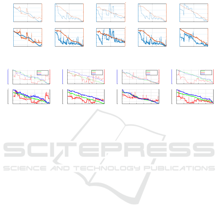
5.2 Two Objectives: NSGA-II
The NSGS-II algorithm, a two-objective optimization
method, was configured with following pair of objec-
tives ( in independent runs ) : i) Area and Delay, ii)
Delay and Leakage Power, iii) Delay and Switching
Power, iv) Delay and Total Power, and v) Delay and
Sum of Total Power. The best candidate solution at
each generation is presented in the top series of the
plots in Figure 7, and all solutions are presented in
the bottom series plot in the same Figure. Within the
1000 evaluations composed of 100 generations and
10 candidates in each generation, it is difficult to find
the optimal point as compared to the single objec-
tive functional run since the candidate solutions ex-
hibit short-term fluctuations for the characterized de-
lay. It is also clearly evident that apart from delay, all
other parameters, including leakage power, switching
power, total power, sum of total power, and area con-
tinue to showcase minuscule fluctuations along the
generations. When the characterized delay shoots up,
Meta-Heuristic Optimization of Transistor Sizing in CMOS Digital Designs
283

2 4 6 8 10 12 14
Area (m
2
)
10
-11
1
1.5
2
2.5
3
3.5
4
Total Power (uW)
GA,ES,PSO,DE
NSGA2
NSGA3
Pareto front
(a)
2 4 6 8 10 12 14
Area (m
2
)
10
-11
0.4
0.5
0.6
0.7
0.8
0.9
1
1.1
1.2
1.3
Delay (ns)
GA,ES,PSO,DE
NSGA2
NSGA3
Pareto front
(b)
0.4 0.5 0.6 0.7 0.8 0.9 1 1.1 1.2 1.3
Delay (ns)
1
1.5
2
2.5
3
3.5
4
Total Power (uW)
GA,ES,PSO,DE
NSGA2
NSGA3
Pareto front
(c)
Figure 9: All 1000 candidate solutions from all 6 algorithms and objectives. The plots present all solutions with characterized
results of (a) Total power versus Area, (b) Delay versus Area, and (c) Total power versus Delay.
the other objective parameters tends to dip and vice-
versa. However, the algorithm tries to minimize delay
in the further generations, along with the other objec-
tives, either power or area. All candidate solutions in
the plot show coherency for the power and area met-
rics but exhibits a large spread in the delay parameter.
This is in accordance with the single objective study,
where the delay and its product objectives continue to
offer diverse solutions till the end. The best candidate
solutions continue to present short-term fluctuations
for the evaluated delay metric, so picking the right
solution for a fixed generation/iterations run is chal-
lenging. One can pick a candidate design solution by
adopting a moving average window along the gener-
ations for the delay. If the current evolved candidate
circuit delay is lower than the moving average, then
the evolution is terminated, and the current candidate
solution is selected in the given evaluation frame. If
otherwise, one can continue to search for an opti-
mized solution. The moving average for a window
length between 5 to 10 appears to be a good choice,
considering runtime and quality of result.
5.3 Three Objectives: NSGA-III
Figure 8 shows the triple objective algorithm runs
with the best solution in top row of plots, and all can-
didate solutions in the bottom row. NSGA-III is con-
figured to optimize the following set of hardware met-
rics: i) Area, Delay and Switching power, ii) Area,
Delay and sum of switching power, iii) Area, De-
lay and total power, and iv) Area, Delay and Sum
of Total power. As expected, power and area follow
a similar trend, but delay exhibits short-term fluctua-
tions, as seen earlier. Hence, a moving average win-
dow aided termination for delay will help in select-
ing the best candidate circuit design after a threshold
number of generations, as discussed previously. The
three-objective runs reiterates the coherency of area
and power parameters and the large spread in delay
along the generations.
6 DISCUSSION
Figure 9 consolidates all the design solutions ex-
tracted from 6 different algorithms across all 100 gen-
erations, along with the pareto-front line. The can-
didate solutions that are among the pareto-front for
the evaluated parameters are coloured in red in the
plots of Figure 9. All 1000 solutions from 8 indi-
vidual objective parameters based single-objective al-
gorithms, 5 pairs of two objective parameters based
NSGA-II algorithm, and 4 pairs of three objective pa-
rameters based NSGA-III are captured in the Figure.
All the solutions are evaluated for area, total power,
and delay. Figure 9 (a) cluster resembles almost a
linear profile between power and area characteristics,
as expected. Hence the optimum solution is the clos-
est point to the origin for minimizing area and power,
also marked in red colour. Figure 9 (b), and 9 (c)
shows the cluster composed of all candidate solutions
evaluated for delay versus area, and total-power ver-
sus delay, respectively. Single-objective algorithms
offer the best solutions for a given objective, ignor-
ing other hardware parameters. Nevertheless, NSGA-
II and NSGA-III offers more candidate solutions that
provide equal weightage to multiple hardware param-
eters. The multi-objective NSGA-II, and NSGA-III al-
gorithm runs targeted toward multiple parameters are
preferred over single-objective algorithm runs that are
targeted towards the product of the same parameters.
This is attributed to the domination of one objective
over another in the single objective algorithm runs,
which is not intended for optimizing towards two ob-
jective parameters. The red-coloured pareto-front line
showcases the best solutions among the cluster of can-
didate solutions. One can select the best solution
along the pareto-front line for the specified margin of
the hardware parameters.
ECTA 2023 - 15th International Conference on Evolutionary Computation Theory and Applications
284

Figure 10: Extracted candidate solutions from all 100 generations and evaluated for total power versus delay with respect
to (a) four single-objective algorithms covering all 8 objectives, (b) 8 different objectives configured on 4 different single-
objective algorithms, (c) five pair of objective runs on NSGA-II algorithm, and (d) four set of objective runs on NSGA-III
algorithm, (e) Single objective GA run for 8 objectives, (f) Single objective ES run for 8 objectives, (g) Single objective PSO
run for 8 objectives, and (h) Single objective DE run for 8 objectives. Best viewed in enlarged size and color.
Figure 10 covers all solutions from different al-
gorithms while segregating with respect to the objec-
tive function. Figure 9 (a) clearly shows that GA de-
rived candidate solutions remain closest to the pareto-
front line among all other single-objective algorithms
when evaluated for characterized total power and de-
lay. Figure 10 (b) showcases the impact of the choice
of the single-objective function evaluated against
Total-Power and Delay. Delay (De) and Product of
Delay-and-Sum-of-Switching-Power (PDSSP) objec-
tives resulted in candidate solutions with minimum
delay. Switching-Power (SP), Sum-of-Switching-
Power (SSP), and Product-of-delay-and-Switching-
Power (PDSP) as objective parameters resulted in
candidate solutions with low power. PDSP-based can-
didate solutions lie close to the pareto-front line, es-
pecially when both delay and total power are given
equal weightage, as shown in Figure 10 (b). Single
objective-based runs result in candidate design so-
lutions highly optimized for either delay or power.
Figure 10 (c) covers the candidate solutions gener-
ated from NSGA-II algorithm runs. As expected, the
candidate solutions generated through the objective
pairs consisting of delay and total power lie on the
pareto-front points marked in red. Figure 10 (d) cov-
ers the candidate solutions generated from NSGA-III
algorithm runs. The best candidate solutions gener-
ated through the objective pairs of Area, Delay, and
Total-Power, lie on the pareto-front points. Addition-
ally, Area, Delay, and Sum of Total-Power targeted
solutions also lie on the pareto-front profile, which
is expected considering Sum of Total-Power involves
worst-case Total-Power measurements.
Interestingly, the shape of the cluster consisting of
candidate solutions generated from single-objective
functions differs from the multi-objective derived
ones when evaluated for the same hardware metrics.
NSGA-II, and NSGA-III solutions move towards the
origin with generations from the randomly seeded
initial circuit. In contrast, the single-objective runs
showed more significant movement towards the bot-
tom and left, along the objective axis. Among the four
single-objective functions, the derived pareto-front
line composed of the best candidate solutions, from
GA showcases the best hardware metrics, as depicted
in the Figure 10 (e, f, g and h). It is also evident that
delay and total-power targeted objective run show-
cases the best solutions when evaluated for the same
hardware parameters for all four single-objective al-
gorithms.
7 CONCLUSIONS
Circuit optimization is one of the common challenges
encountered by designers. An ad-hoc usage of opti-
mization algorithms has been employed without com-
prehensive evaluation. The proposed work evaluates
Meta-Heuristic Optimization of Transistor Sizing in CMOS Digital Designs
285

six popular algorithms (GA, ES, DE, PSO, NSGA-II,
NSGA-III) based on the impact from objective of op-
timization, sparsity presented by the evolved candi-
date solutions along the generations, diversity in hard-
ware metrics of the candidate solutions, and mono-
tonicity in convergence. All the algorithms were eval-
uated using FA design consisting of 28 transistors.
Among the single-objective runs for the same num-
ber of evaluations, GA generates the most optimized
circuit design solution and continues offering diverse
solutions along the runs. ES comes close to GA and
has a larger search space. PSO lacks diversity in so-
lutions and is influenced by the best candidate in ev-
ery generation. DE exhibits rapid initial convergence
with poor hardware metrics. One can adopt GA al-
gorithm over NSGA-II, and NSGA-III if the objectives
and their importance are defined for the circuit under
design. However, if the targeted parameter weigh-
tages are not known or equal importance is recom-
mended, then NSGA-II or NSGA-III are preferred over
single-objective functions. This work aids in optimiz-
ing custom circuits and higher-order custom standard
cells by adopting the most effective algorithm given
the specified metrics range and evolution runs. The
thorough investigation shows that a robust optimiza-
tion of CMOS-based custom digital circuits is possi-
ble with a thorough characterization, irrespective of
the technology progression, provided PDKs and in-
terconnect models are made available.
REFERENCES
(2022). Librecell. https://codeberg.org/tok/librecell.
Abazyan, S. (2021). Standard cell library enhancement
for mixed multi-height cell design implementation.
In 2021 IEEE East-West Design & Test Symposium
(EWDTS), pages 1–4.
Abazyan, S., Melikyan, S., and Musayelyan, D. (2021).
Standard cell library enhancement using neural net-
work based sleep mode control integration for low
leakage designs. In 2021 IEEE East-West Design &
Test Symposium (EWDTS), pages 1–4.
Cao, L., Bale, S. J., and Trefzer, M. A. (2018). Instrument-
ing parametric physical layout for multi-objective op-
timisation. In 2018 IEEE Symposium Series on Com-
putational Intelligence (SSCI), pages 1339–1345.
Cao, L., Bale, S. J., and Trefzer, M. A. (2021a). Multi-
objective digital design optimization via improved
drive granularity standard cells. IEEE Transactions on
Circuits and Systems I: Regular Papers, 68(11):4660–
4671.
Cao, L., Bale, S. J., and Trefzer, M. A. (2021b). Multi-
objective optimisation of digital circuits based on cell
mapping in an industrial eda flow.
Conesa-Mu
˜
noz, J., Ribeiro, A., Andujar, D., Fernandez-
Quintanilla, C., and Dorado, J. (2012). Multi-path
planning based on a nsga-ii for a fleet of robots to
work on agricultural tasks. In 2012 IEEE Congress
on Evolutionary Computation, pages 1–8.
Deb, K. and Jain, H. (2014a). An evolutionary many-
objective optimization algorithm using reference-
point-based nondominated sorting approach, part i:
Solving problems with box constraints. IEEE Trans-
actions on Evolutionary Computation, 18(4):577–
601.
Deb, K. and Jain, H. (2014b). An evolutionary many-
objective optimization algorithm using reference-
point-based nondominated sorting approach, part i:
Solving problems with box constraints. IEEE Trans-
actions on Evolutionary Computation, 18(4):577–
601.
Dey, S., Nandi, S., and Trivedi, G. (2021). Machine learn-
ing for vlsi cad: A case study in on-chip power grid
design. In 2021 IEEE Computer Society Annual Sym-
posium on VLSI (ISVLSI), pages 378–383.
Eriksson, H., Larsson-Edefors, P., Henriksson, T., and
Svensson, C. (2003). Full-custom vs. standard-cell de-
sign flow - an adder case study. In Proceedings of the
ASP-DAC Asia and South Pacific Design Automation
Conference, 2003., pages 507–510.
Gu, X., Wang, X., Liu, Z., Zha, W., Xu, X., and Zheng, M.
(2020). A multi-objective optimization model using
improved nsga-ii for optimizing metal mines produc-
tion process. IEEE Access, 8:28847–28858.
H C, P. and Rao, M. (2022). Evolutionary standard cell syn-
thesis of unconventional designs. In Proceedings of
the Great Lakes Symposium on VLSI 2022, GLSVLSI
’22, page 189–192, New York, NY, USA. Association
for Computing Machinery.
Hong, J., Kim, S., and Jeon, D. (2022). An automatic cir-
cuit design framework for level shifter circuits. IEEE
Transactions on Computer-Aided Design of Integrated
Circuits and Systems, pages 1–1.
Innocenti, J., Julien, F., Portal, J., Lopez, L., Hubert, Q.,
Masson, P., Sonzogni, J., Niel, S., and Regnier, A.
(2015). Layout optimizations to decrease internal
power and area in digital cmos standard cells. In
2015 38th International Convention on Information
and Communication Technology, Electronics and Mi-
croelectronics (MIPRO), pages 1582–1587.
Ishibuchi, H., Imada, R., Setoguchi, Y., and Nojima, Y.
(2016). Performance comparison of nsga-ii and nsga-
iii on various many-objective test problems. In 2016
IEEE Congress on Evolutionary Computation (CEC),
pages 3045–3052.
Jo, K., Ahn, S., Do, J., Song, T., Kim, T., and Choi, K.
(2019). Design rule evaluation framework using auto-
matic cell layout generator for design technology co-
optimization. IEEE Transactions on Very Large Scale
Integration (VLSI) Systems, 27(8):1933–1946.
Kashfi, F., Hatami, S., and Pedram, M. (2011). Multi-
objective optimization techniques for vlsi circuits. In
2011 12th International Symposium on Quality Elec-
tronic Design, pages 1–8.
Lim, S. H., Lim, Y. W., Mashohor, S., Kamsani, N. A.,
Sidek, R. M., Hashim, S. J., and Rokhani, F. Z. (2017).
ECTA 2023 - 15th International Conference on Evolutionary Computation Theory and Applications
286

Generating power-optimal standard cell library speci-
fication using neural network technique. In 2017 IEEE
Asia Pacific Conference on Postgraduate Research in
Microelectronics and Electronics (PrimeAsia), pages
101–104.
Matos, J. M., Carrabina, J., and Reis, A. (2019). Efficiently
mapping vlsi circuits with simple cells. IEEE Trans-
actions on Computer-Aided Design of Integrated Cir-
cuits and Systems, 38(4):692–704.
Mezzomo, C., Bajolet, A., Cathignol, A., Frenza, R., and
Ghibaudo, G. (2011). Characterization and model-
ing of transistor variability in advanced cmos tech-
nologies. Electron Devices, IEEE Transactions on,
58:2235 – 2248.
Nikoubin, T., Bahrebar, P., Pouri, S., Navi, K., and Iravani,
V. (2010). Simple exact algorithm for transistor siz-
ing of low-power high-speed arithmetic circuits. VLSI
Design, 2010.
Pang, L. M., Ishibuchi, H., and Shang, K. (2020). Nsga-ii
with simple modification works well on a wide variety
of many-objective problems. IEEE Access, 8:190240–
190250.
Paul, P., Baishnab, K., Laskar, N. M., and Talukdar, F.
(2015). Particle swarm optimization in designing of
high slew rate and improved resolution cmos winner-
take-all (wta) circuit suitable for attention shift. In
2015 6th International Conference on Information
and Communication Systems (ICICS), pages 55–59.
Rahman, M., Tennakoon, H., and Sechen, C. (2013).
Library-based cell-size selection using extended logi-
cal effort. IEEE Transactions on Computer-Aided De-
sign of Integrated Circuits and Systems, 32(7):1086–
1099.
Sasikumar, A. and Muthaiah, R. (2017). Operational ampli-
fier circuit sizing based on nsga-ii and particle swarm
optimization. In 2017 International Conference on
Networks & Advances in Computational Technologies
(NetACT), pages 64–68.
Srinivas, N. and Deb, K. (1994). Muiltiobjective opti-
mization using nondominated sorting in genetic algo-
rithms. Evolutionary Computation, 2(3):221–248.
Xiaoqing, L., Haiying, D., Hongwei, L., Mingxue, L., and
Zhiqiang, S. (2019). Optimization control of front-
end speed regulation (fesr) wind turbine based on im-
proved nsga-ii. IEEE Access, 7:45583–45593.
Zhan, Z.-H., Zhang, J., Li, Y., and Chung, H. S.-H. (2009).
Adaptive particle swarm optimization. IEEE Transac-
tions on Systems, Man, and Cybernetics, Part B (Cy-
bernetics), 39(6):1362–1381.
Zheng, L. M., Zhang, S. X., Zheng, S. Y., and Pan, Y. M.
(2016). Differential evolution algorithm with two-
step subpopulation strategy and its application in mi-
crowave circuit designs. IEEE Transactions on Indus-
trial Informatics, 12(3):911–923.
Meta-Heuristic Optimization of Transistor Sizing in CMOS Digital Designs
287
