
Analysis and Improvement of Oscilloscope Jitter Measurement Floor
Based on Simulation Experiments
Jiangmiao Zhu, Yufen Sun, Kaige Man, Yidi Wang and Yifan Wang
Beijing University of Technology, Beijing, China
Keywords: Oscilloscope, Clock Jitter, Inherent Noise, Jitter Measurement Floor, Simulation Experiment.
Abstract: Oscilloscopes are crucial universal instruments in the fields of electronic information and communication,
capable of making time-domain measurements of signals and systems. Due to imperfect hardware,
oscilloscopes exhibit a certain jitter. This paper refers to the jitter originating from the oscilloscope itself is
called the oscilloscope jitter measurement floor. During the process of measuring signal jitter using an
oscilloscope, the jitter measurement floor inevitably affects the measurement results, introducing errors. This
paper primarily investigates factors influencing the oscilloscope jitter measurement floor, including the
oscilloscope’s sampling clock jitter, inherent noise, and input signal frequency,etc.. Simultaneously, the
impact of these factors on oscilloscope measurement results is assessed, and experimental verification is
conducted using an oscilloscope simulation platform. Finally, methods for reducing the oscilloscope jitter
measurement floor are proposed.
1 INTRODUCTION
The definition of jitter varies slightly across different
fields, leading to inconsistencies in the definitions
provided by international organizations and
institutions such as the International Electrotechnical
Commission (IEC), Institute of Electrical and
Electronics Engineers (IEEE), and American
National Standards Institute (ANSI), etc.(Std, I.-
Peterich, D.),. This paper adopts the latest standard
for defining jitter as provided by IEEE in 2020, i.e.,
jitter is the deviation between the actual time of a set
of events and their ideal values (Std, I., Zhu
Jiangmiao).
Jitter is a measure of short-term uncertainty in the
time domain of a signal and is assessed using phase
noise in the frequency domain to measure the short-
term instability of the signal. Oscilloscopes are
indispensable for time-domain measurement and
analysis of signals. However, due to the presence of
oscilloscope jitter measurement floor, the measured
jitter results inevitably contain errors other than the
signal jitter. If the signal jitter is significantly greater
than the oscilloscope jitter measurement floor, then
these errors can be neglected. However, if the above
requirement is not met, the oscilloscope jitter
measurement floor will cause significant errors,
thereby affecting the accuracy of the measurement
results. Therefore, it is of great importance to identify
the factors contributing to the oscilloscope jitter
measurement floor, understand how these factors
affect the measurement results, and minimize their
impact in order to study oscilloscope measurement.
Oscilloscopes can be categorized as analog
oscilloscopes and digital oscilloscopes. With
technological advancements, analog oscilloscopes
have been gradually replaced by digital oscilloscopes,
and digital oscilloscopes can further be classified into
sampling oscilloscopes and real-time oscilloscopes.
Sampling oscilloscopes are also known as
communication signal analyzers. However, whether it
is a sampling oscilloscope or real-time oscilloscope,
the components such as analog-to-digital converter
(ADC), attenuators and amplifiers in the analog front-
end, are vital for their operation.
The primary sources contributing to the
oscilloscope jitter measurement floor are the
sampling clock jitter in the ADC, oscilloscope's
analog front-end and digital processing. On the basis
of clarifying how the above factors affect the
oscilloscope jitter measurement floor is crucial for
effectively reducing their impact on the measurement
results.
Zhu, J., Sun, Y., Man, K., Wang, Y. and Wang, Y.
Analysis and Improvement of Oscilloscope Jitter Measurement Floor Based on Simulation Experiments.
DOI: 10.5220/0012284700003807
Paper published under CC license (CC BY-NC-ND 4.0)
In Proceedings of the 2nd International Seminar on Artificial Intelligence, Networking and Information Technology (ANIT 2023), pages 391-396
ISBN: 978-989-758-677-4
Proceedings Copyright © 2024 by SCITEPRESS – Science and Technology Publications, Lda.
391

2 SAMPLING PRINCIPLE OF
SAMPLING OSCILLOSCOPE
An oscilloscope is an electronic instrument that
converts electrical signals, primarily voltage, into
visible traces on a display screen. In other words, an
oscilloscope can convert electrical signals into optical
signals and dynamically plot the electrical signals in
a two-dimensional form over time. The voltage is
plotted on the vertical axis of the oscilloscope display
screen, while the time is plotted on the horizontal axis.
The plotted voltage and time are ultimately displayed
as a graph of the input signal, often referred to as a
"waveform". As the characteristics of the input signal
change, the displayed waveform on the oscilloscope
screen is continuously updated.
The bandwidth range of a sampling oscilloscope
is much wider than that of a real-time oscilloscope,
meaning it can measure signals with a broader
bandwidth range. Due to the high frequency of the
input signal, the oscilloscope does not directly display
the measured signal. Instead, it uses a frequency-
conversion method to sample the signal at different
positions in the waveform of the measured signal,
using a time much shorter than the period of the
measured signal. The sampling is performed
sequentially in a stepped order for each waveform of
the signal (Wang Shibiao).
PRBS
1 2 3
Re-arm time
15bit
Trigger point
Sampling point
Sequential delay
Reconstructed
waveform
Pattern
trigger
Fig. 1. Schematic diagram of sampling principle of
sampling oscilloscope-
Taking PRBS code as an example, Fig 1 illustrates
the sampling principle of a sampling oscilloscope. A
trigger point is provided by a pattern trigger from the
clock signal, and sampling is performed after the
trigger. After each pattern trigger, new sampling is
carried out at sampling points slightly away from the
pattern trigger point and repeated. Then, the sampled
oscilloscope reconstructs the waveform. This paper
focuses on studying the jitter of sampling
oscilloscopes, and the oscilloscopes mentioned
following the paper refer to digital sampling
oscilloscopes unless otherwise specified.
3 SAMPLE CLOCK JITTER
The sampling clock is an essential part of ADC. The
sampling oscilloscope through the ADC to sample the
input signal, and then converting each sample point
of the analog signal into a digital value. The sampling
clock controls when the ADC performs the sampling.
In other words, the frequency of the sampling clock
determines the time interval of the oscilloscope.
However, the clock signal generated by the sampling
clock itself exhibits a certain jitter, which is referred
to as clock jitter. Clock jitter is an inherent
characteristic that cannot be completely eliminated (S.
Huang) and is one of the main sources of the
oscilloscope jitter measurement floor.
Clock jitter can be classified into random jitter and
deterministic jitter. Random jitter is caused by
thermal noise, flicker noise, and shot noise, which are
related to the electronic and hole characteristics of
electronic and semiconductor devices. The sources of
deterministic jitter are switching power supply noise,
crosstalk, and electromagnetic interference, etc.,
which are related to circuit design (LI Liping, Zhang
Changjun).
Clock jitter can be represented in various ways
(Zhu Jiangmiao), such as Period jitter (PEJ), Cycle to
Cycle jitter (C2C), and Timing Error (TE). In this
paper, TE is used to represent clock jitter, which
refers to the deviation between the actual edge of the
clock and the ideal edge. Fig 2 gives the schematic
diagram of TE.
Fig. 2. Schematic diagram of TE in clock jitter.
Due to the high sampling clock frequencies of
modern high-bandwidth oscilloscopes, which can
reach up to 160G/s or higher, the time interval
between samples is very small. Therefore, ensuring
that each actual sample point falls at the ideal position
is challenging. In other words, the existence of clock
jitter causes the sampled amplitude of the signal to not
correspond exactly to its actual sampling time,
thereby affecting the measurement results of the
oscilloscope. Since clock jitter includes both
deterministic jitter and random jitter, averaging
multiple waveforms can effectively remove the
random jitter in clock jitter, reducing the magnitude
ANIT 2023 - The International Seminar on Artificial Intelligence, Networking and Information Technology
392

of clock jitter. Fig 3 illustrates the impact of clock
jitter on the measurement results through simulation
experiments. In the figure 3, a represents the input
signal measured by the oscilloscope without
waveform averaging, and b represents the input signal
measured by the oscilloscope with waveform
averaging.
a)
b)
Fig. 3. Schematic diagram of measurement results with and
without clock jitter.
Therefore, to ensure that the deviation between
the actual sampling time and the ideal sampling time
of each sampling point instant, i.e. TE, as small as
possible, is a critical task to improve the measurement
accuracy of the oscilloscope. However, regardless of
technological advancements, the jitter value will
never be zero due to the inherent characteristics of the
hardware equipment.
4 INHERENT NOISE
The noise in the analog front-end and digital
processing of an oscilloscope is also one of the
sources of jitter measurement floor, which is referred
to as inherent noise in this article. In addition to
introducing amplitude measurement errors, the
inherent noise of an oscilloscope can also cause
changes in the threshold crossing time of the signal,
resulting in jitter (M. Shimanouchi, 2001).The
schematic diagram illustrating the specific impact of
inherent noise on jitter measurement floor is shown in
Figure 4. Next, we will separately discuss the noise in
the digital processing of the oscilloscope and the
noise generated by the analog front-end.
Figure 4: Schematic diagram showing the impact of noise
on jitter measurement floor.
4.1 Quantization Noise
Quantization error in the digital processing of an
oscilloscope is also known as quantization noise,
which is introduced by the oscilloscope's analog-to-
digital converter (ADC) and is mainly related to the
resolution and performance of the ADC.
According to the principles of sampling and
quantization in a sampling oscilloscope, the
resolution of the ADC chip directly determines the
vertical sampling accuracy of the oscilloscope. For
example, if the ADC conversion chip is 8-bit, the
vertical signal can be divided into 256 segments and
then quantized. Assuming the input signal amplitude
is 1V, the quantization accuracy is 1V/256, which
means the ADC can only distinguish voltage signals
greater than 1/256V. if the ADC conversion chip is
10-bit, the vertical signal can be divided into 1024
segments, and keep the input signal amplitude still at
1V, the quantization accuracy becomes 1V/1024,
meaning the ADC can distinguish voltage signals
greater than 1/1024V. It can be seen that the higher
the number of bits of the ADC chip in the oscilloscope,
the higher the vertical resolution and the smaller the
quantization noise of the oscilloscope. However, for
the same oscilloscope, the number of quantization
bits is generally constant, and therefore its
quantization noise is also fixed.
Analysis and Improvement of Oscilloscope Jitter Measurement Floor Based on Simulation Experiments
393
4.2 Noise Generated by the Analog
Front-End of the Oscilloscope
The noise generated by the analog front-end of the
oscilloscope is mainly caused by the attenuator and
the preamplifier. The analog-to-digital converter
(ADC) cannot distinguish between signal and noise
during sampling, so when the signal is amplified, the
noise will also be amplified. The amplification factor
of the attenuator and preamplifier is not fixed,
resulting in the variability of this noise.
The attenuator and preamplifier of the
oscilloscope can be used to control and adjust the
vertical sensitivity of the oscilloscope, which is an
important component in the front-end circuit of the
oscilloscope, allowing users to select different
sensitivity ranges for the signal to accommodate input
signals with different amplitudes. Therefore, the
vertical sensitivity setting of the oscilloscope and the
amplitude of the input signal can affect the noise
generated by the analog front-end of the oscilloscope
and then affect the jitter measurement floor. To verify
this conclusion, this article uses simulation
experiments to verify the influence of vertical
sensitivity setting and input signal amplitude on the
jitter measurement floor.
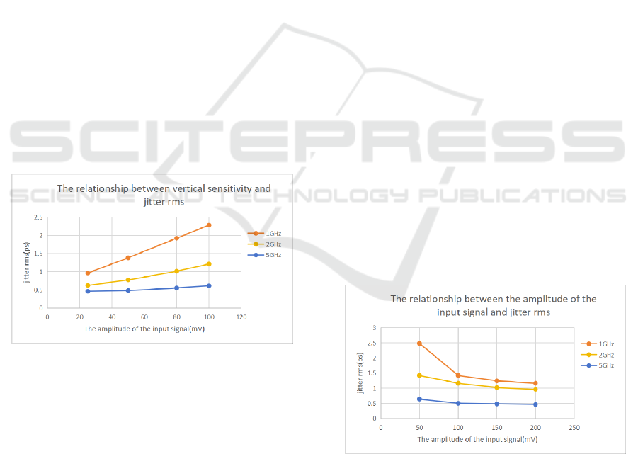
1) Influence of Vertical Sensitivity on jitter
measurement floor
Figure 5: Relationship between vertical sensitivity and jitter
rms.
First, a sinusoidal signal with a jitter value of 400
fs is inputted into the simulation software. In the case
of other parameters remain unchanged, the vertical
sensitivity is adjusted and the number of measuring
result (jitter rms) at different vertical sensitivities are
recorded. To avoid experimental variability, multiple
signals with different frequencies are tested, and
multiple sets of data are recorded and plotted. As
shown in Figure 5, regardless of the change in signal
frequency, the oscilloscope's jitter measurement
results decrease as the vertical sensitivity increases. It
should be noted that a higher numerical value of the
vertical sensitivity indicates lower sensitivity. As the
vertical sensitivity decreases, the oscilloscope
measurement results increase. However, the input
signal jitter remains unchanged, indicating that the
jitter measurement floor of the oscilloscope is
increasing, and the trend is consistent with the change
in the measured results in Figure 5.
When the vertical sensitivity decreases, the noise
increases, resulting in an increase in the jitter
measurement floor of the oscilloscope. Therefore,
when using an oscilloscope to measure a signal, it is
advisable to fill the waveform on the oscilloscope
screen as much as possible to reduce the jitter
measurement floor.
2) Influence of Input Signal Amplitude on jitter
measurement floor
To investigate the influence of input signal
amplitude on the jitter measurement floor of the
oscilloscope, the vertical sensitivity of the
oscilloscope is kept constant while changing the input
signal amplitude. Experimental data is recorded and
plotted. As shown in Figure 6, it can be observed that
under the condition of constant vertical sensitivity,
the smaller the signal amplitude, the larger the jitter
measurement result of the oscilloscope. Similarly, the
input signal jitter remains unchanged. This indicates
that the jitter measurement floor increases. This is
because the smaller the signal amplitude, the larger
the amplification factor, and the more severe the
effect of noise. However, this does not mean that a
larger signal amplitude is always better, as once the
signal amplitude exceeds the measurement range of
the oscilloscope, the measurement result will be
invalid.
Figure 6: Relationship between the amplitude of input
signal and jitter rms.
In conclusion, the inherent noise of an
oscilloscope mainly consists of the two factors
mentioned above. The quantization noise is fixed for
a given oscilloscope, while the impact of oscilloscope
ANIT 2023 - The International Seminar on Artificial Intelligence, Networking and Information Technology
394

analog front-end noise on jitter is related to the
vertical sensitivity and input signal amplitude of the
oscilloscope. A higher vertical sensitivity setting of
the oscilloscope results in a smaller noise, and vice
versa. Within the measurement range of the
oscilloscope, a larger input signal amplitude leads to
a smaller noise. Therefore, when measuring the input
signal, the vertical sensitivity of the oscilloscope can
be adjusted to make the vertical sensitivity as large as
possible when the signal is displayed completely on
the oscilloscope.
5 INPUT SIGNAL FREQUENCY
In addition to the factors mentioned above, the
frequency of the input signal during actual
measurement will also have an impact on jitter. By
keeping the input signal jitter and vertical sensitivity
constant, the frequency of the input signal is changed,
and the measurement results are recorded. Figure 7
shows the relationship between input signal
frequency and measurement results of oscilloscope in
the simulation experiment.
Figure 7: Relationship between the frequency of input
signal and jitter rms.
According to Figure 7, it can be observed that as
the input signal frequency increases, the jitter
measurement results (jitter rms) of the oscilloscope
decrease. This is because the higher the frequency of
the input signal, the faster the signal conversion rate,
and the less the impact of noise superimposed on the
time axis. The specific impact is illustrated in Figure
8. In other words, the influence of inherent noise on
the measurement results decreases with higher input
signal frequency. This also demonstrates the effect of
the oscilloscope's inherent noise on the jitter
measurement floor.
Figure 8: Schematic diagram of the impact of signal slope
on jitter measurement floor.
6 CONCLUSION
Based on the theoretical analysis and simulation
studies, we can conclude that the jitter measurement
floor of an oscilloscope is affected by the
oscilloscope's sampling clock jitter, inherent noise,
and input signal frequency. The sampling clock jitter
is beyond the control of users, thus the oscilloscope
manufacturers require continuous optimization of its
circuit design and hardware equipment to minimize
its jitter value. The quantization noise in the inherent
noise of an oscilloscope is related to the resolution of
the ADC conversion chip. Higher resolution leads to
smaller quantization errors, which is also the reason
why many oscilloscope manufacturers have been
continuously improving the ADC resolution in recent
years.
It can be verified by experiments that the analog
front-end noise in the inherent noise, under the
condition of constant input signal, is closely related
to the vertical sensitivity setting of the oscilloscope
and the input signal frequency. In many cases, the
impact of analog front-end noise on jitter
measurement floor is much greater than other factors.
Therefore, selecting the appropriate vertical
sensitivity during the measurement process is one of
the important means to reduce the oscilloscope jitter
measurement floor. After reducing the jitter
measurement floor, its contribution to the
oscilloscope measurement results will
correspondingly decrease.
ACKNOWLEDGMENT
This work is supported by Key Special Project
“Broadband Sampling Oscilloscope” on National
Key Research and Development Program of
“Fundamental Research Conditions and
Development of Major Scientific Instruments”. No.
2022YFF0707104.
Analysis and Improvement of Oscilloscope Jitter Measurement Floor Based on Simulation Experiments
395

REFERENCES
Std, I., IEEE Standard for Terminology and Test Methods
for Analog-to-Digital Converters(S). IEEE, 2011.
M Komárek, and J Roztočil. Selecting Sinewave Test
Frequencies for Dynamic ADC Tests (J).
Instrumentation for the ICT. 2010, 528-532.
Peterich, D., Ham, B., Van, S., Edward, D. & Grivna, L.
Fibre Channel- Methodologies for Jitter and Signal
Quality Specification(S). 2003.
Std, I., IEEE Standard for Transitions, Pulses, and Related
Waveforms(S). IEEE, 2011.
Zhu Jiangmiao, Sun Yufen, Chen Junyu. Measurements and
Calculation Methods of Jitter in Broadband Sampling
Oscilloscope(C). 16th International Conference on
Electronic Measurement & Instruments. 2023, 81-85.
Wang Shibiao. Research of Key Techniques for Time
Domain Calibration of Broadband Sampling
Oscilloscope (D). Beijing University of Technology,
2019.
J. Towfic, S. -K. Ting, A. H. Sayed. Sampling clock jitter
estimation and compensation in ADC circuits(C).
Proceedings of 2010 IEEE International Symposium on
Circuits and Systems, 2010, 829-832.
J. Elbornsson, F. Gustafsson, J.-E. Eklund. Blind adaptive
equalization of mismatch errors in a time-interleaved
A/D converter system (J). IEEE Transactions on
Circuits and Systems I. Vol. 51, no. 1, Jan. 2004, 151–
158.
C. Fu, H. Wang. Adaptive optimization in A/D converter
system(C), 6th IEEE International Conference on
Industrial Informatics. July 2008, 627–630.
S. Huang, B. Levy. Blind calibration of timing offsets for
fourchannel time-interleaved ADCs (J). IEEE
Transactions on Circuits and Systems I. Vol. 54, no. 4,
April 2007, 863–876.
LI Liping. Jitter Analysis in High-speed Serial
Interconnection (D). Xidian University, 2010.
Zhang Changjun. Basic series of signal integrity Analysis -
- Clock jitter Measurement and Analysis (J). Foreign
Electronic Measurement Technology, 2010, 7-11.
Johnnie Hancock Agilent Technologies. Regonize the
Noise and its Influence on Oscilloscope Measurement
(J). Electronics Quality. 2005, 17-20.
M. Shimanouchi. An approach to consistent jitter modeling
for various jitter aspects and measurement methods(C).
Proceedings International Test Conference 2001, 848-
857.
ANIT 2023 - The International Seminar on Artificial Intelligence, Networking and Information Technology
396
