
The Design of High Speed Wideband Receiver Based on FPGA
Bin Yao
1
, Zitao Huang
1
, Juan Yang
2
, Meng Li
1
and Yunan Guo
1
1
Beijing Orient Institute of Measurement & Test, Beijing, China
2
High-tech Institute, FanGong-ting South Street on the 12th, QingZhou, ShanDong, China
Keywords: Software Defined Radio, High-Speed ADC, JESD204B, Digital Down Conversion, FPGA.
Abstract: Analog frequency conversion and digital if sampling are adopted in the traditional design of receivers. This
architecture has disadvantages of hardware complexity and low sampling rate. This paper proposes a design
of high speed wideband receiver based on FPGA, which reduces system complexity. All parameters and
algorithms applied in the design were firstly tested in Matlab. Then they were implemented on a hardware
built by high-speed ADC and FPGA. Finally, the signal generator and spectrum analyzer are used to analyze
the system performance. The results verify that the digital receiver platform can correctly recover the bit in-
formation at the sending end, and prove that the design can correctly demodulate data and meet the system
requirements.
1 INTRODUCTION
Software radio is a new architecture based on A/D
converters and FPGA/DSP (Pupalaikis P J., 2007). It
is based on software as the core, and the traditional
receiver design implements analog frequency
conversion and digital intermediate frequency
sampling methods. This design has the
disadvantages of complex structure, low sampling
rate, narrow bandwidth, and lack of flexibility.
The software radio receiver system designed in
this paper directly samples wideband RF (Lee K,
2005) signals using high sampling rate, which uses
JESD204B interface to send the high speed serial
signal into FPGA, then sends the processed data to
the host computer through Ethernet after channel
selection and digital down-conversion carried out on
FPGA. The test results show that the system has
simple structure, high integration, portability, good
universality and practicability.
2 SYSTEM IMPLEMENTATION
2.1 Overall Design
Parameters of RF signal are as follows. The
bandwidth of RF signal is 50M, the central
frequency is 2100MHz, there are 1800 narrowband
signals in the band-width, the narrowband signal
number rate is 16KHz, the bandwidth is 24K, and
the modulation mode is BPSK, QPSK, 8BPSK
(Middleton R J C., 2012).
The digital receiver consists of AD sampling
module and FPGA module. The analog RF signal is
sampled by bandpass sampling. The sampling signal
spectrum is obtained by periodization of the
continuous signal spectrum at sampling rate
intervals. Consider the bandwidth of RF signals, data
processing capacity after sampling and sampling rate
of output signals after down-sampling, the sampling
rate was set to 1536MHz. After the RF signal is
sampled at 1536MHz, the 2100MHz carrier signal in
the analog domain is transformed into the 564MHz
if signal in the digital domain.
The signal is down-sampled and filtered in AD,
its sampling rate becomes 192MHz, and the signal is
fed into FPGA. FPGA implements channel selection
and digital down conversion, then down-sample the
digital signal to 240KHz. The digital down
conversion is composed of DDS (direct digital
frequency synthesizer), multiplier, low pass filter
and decimation filter. The clock of FPGA is 192
MHz, it requires a filter of order 88304 to filter
signals, which can’t be realized. Therefore, the
signal needs to be down-sampled and filtered. After
25*32 times of down-sampling, the final sampling
rate is reduced to 240 KHz. Using Matlab to send
BPSK signal according to the above parameters for
simulation, to obtain the frequency domain and time
454
Yao, B., Huang, Z., Yang, J., Li, M. and Guo, Y.
The Design of High Speed Wideband Receiver Based on FPGA.
DOI: 10.5220/0012285800003807
Paper published under CC license (CC BY-NC-ND 4.0)
In Proceedings of the 2nd International Seminar on Artificial Intelligence, Networking and Information Technology (ANIT 2023), pages 454-457
ISBN: 978-989-758-677-4
Proceedings Copyright © 2024 by SCITEPRESS – Science and Technology Publications, Lda.
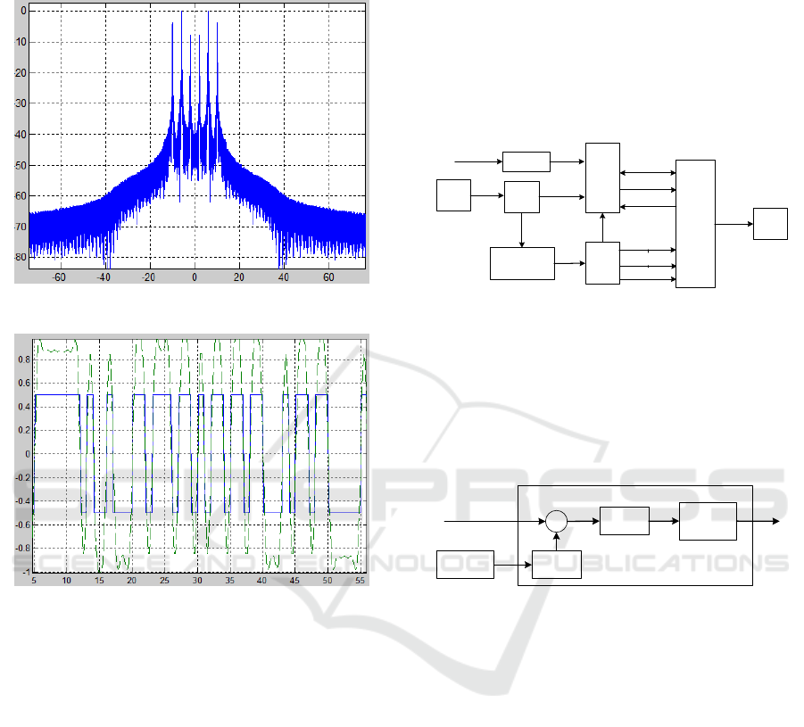
domain waveform of the receiver output signal are
shown in figure1 and figure2.
Figure 1. Spectrum of output signal.
Figure 2. Waveform of output signal.
2.2 System Hardware Design
The hardware architecture is shown in figure 3.
The matching circuit can match the input signal
with the input impedance of the amplifier. The
system uses TI's ADC12J4000 chip, which is A
single-channel, low-power 12-bit A/D converter
with A maximum sampling frequency of 4GHz. The
ADC sampling clock is 1536MHz, and several
internal registers are set through the SPI interface of
FPGA to realize frequency shift, 8 times down-
sampling and filtering. The sampled signal transmits
through the JESD204B interface and sends the high-
speed differential signal to the FPGA. The
JESD204B interface has many advantages, such as
no data interface clock, no need for a large number
of IO ports, convenient wiring. FPGA module
adopts xc7k325tffg900 chip of kintex-7 series of
Xilinx company, and the clock of FPGA is shown in
figure 3. GTXREF_P/N, FPGA_REF_A_P/N are the
system clock and reference clock of the JESD
module in FPGA, and FPGA_REF_B_P/N are the
sampling clock of the signal in FPGA. Through the
internal JESD interface, FPGA converts the input
high-speed AD signal into a signal with a sampling
rate of 192MHz with the bit width of 12bit. After the
signal passes through the digital signal processing
module in FPGA, it is sent to the host computer via
UDP.
OCXO
Clock
PLL
DEVCLK_P/N
ADC
DIVIDER/8
PLL
FPGA_REF_A_P/N
GTX
FPGA
SYSREF_P/N
FPGA_REF_B_P/N
Ethernet
Host
Computer
SPI
SYNC
Matching
Circuit
Analog
signal
GTXREF_P/N
Figure 3. Hardware architecture.
2.3 FPGA Module
FPGA implements channel selection in broadband
signals and digital down-conversion (Parhi K K.,
2007), which converts digital signals to baseband, as
shown in figure 4.
DDS
Channel
Selection
CIC
Multi-
stage HB
Filter
×
Input Signal
Figure 4. Block diagram of FPGA module.
1) Channel selection
After ADC sampling, the whole frequency band of
the system is received, with a bandwidth of 50MHz.
For a communication user, only a very narrow
channel is occupied. The channel bandwidth is
20KHz, and there are 200 channels in the whole
broadband. Therefore, we have to select a
narrowband signal that needs to be processed from
the whole broadband signal. Take a narrowband
channel as an example. The narrowband signal
center frequency out is 73MHz, the sampling rate fs
is 192MHz, and the phase bit width of DDS is 32
bits. The frequency control word can be obtained
from the following equation:
sout
ff /2*
32
(1)
The obtained frequency control word is
32'd671088640. According to equation (1), the
corresponding frequency of 200 channels in the
broadband is converted into the corresponding
The Design of High Speed Wideband Receiver Based on FPGA
455

frequency control word and stored in the ROM of
FPGA, as shown in table 1.
Table 1. Three Scheme comparing.
Adress
Channel
0
1
4D52316D
1
2
4D5990DD
……
……
……
1799
1800
754BA3B4
2) Digital down conversion
The channel selection module sends the frequency
control word parameter corresponding to the
specified channel, which controls the DDS module
to produce a spurious dynamic range of 95,
frequency resolution of 0.045, and a 16-bit sine
signal of the same frequency as the input channel,
and multiplies the two to convert the input channel
to the baseband.
In the design of the digital down-conversion part,
the main operation focuses on the down-sampling
and filtering of baseband signals. After the AD
sampling signal is converted to the baseband, the
bandwidth is 24KHz and the sampling rate is fs
192MHz. If the filter is directly filtered, the order of
the filter is too high, so it is necessary to down-
sample the filter and reduce the filter order step by
step.
The decimation filter module is shown in figure
5. The signal first passes through the CIC filter, then
passes through the multistage semi-band extraction
filter, and finally passes through the shaping filter.
CIC
Fs=192M Fs=7.68M
5-stage
HB
PFIR
Fs=0.24M
Fs=0.24M
Figure 5. Decimation filter module.
Design index of CIC filter: the sampling rate Fs
is 192MHz, the maximum passband attenuation shall
not exceed 3dB, and the stopband attenuation shall
not be lower than 60dB. After 25 times of down-
sampling, the passband cutoff frequency relative to
the low sampling rate is less than 1/128. According
to the references, CIC filters with order N = 3,
differential delay M = 1 and down-sampling of 25
can completely meet the requirements. According to
reference 4, the word length equation of FPGA
implementation of CIC filter is given as follows:
in
BRMNB )(2log
max
(2)
Where, B
in
is the input filter data bit width of 16
bits, R is the extraction multiple of 25, and M is the
differential delay of 1. According to equation (2),
the maximum bit width of each operation of CIC
filter is 29 bits. In implementation, in order to
simplify the code, the bit width of each filter is kept
at 29 bits until the final output of CIC filter is
saturated and taken as the final output to the next
module.
Half-band filter design index: Transition band
aliasing is allowed, the sampling rate Fs is 7.68MHz,
the filter passband bandwidth fp is 24K, the
passband tolerance and stopband tolerance are 0.001.
According to calculation, the system uses five-stage
half-band filter cascade to realize filtering, and the
system sampling rate is reduced to 240KHz. The
coefficients of stage 1 to stage 4 semi-band filters
are order 7, and the coefficients of the fifth-order
semiband filter are order 11. After saturation of the
output data bit width of each filter, the output is
16bit.
Shape filter design index: The sampling rate Fs is
240KHz, the filter passband bandwidth fp is 24K,
the passband cut-off frequency Fs =34K, the
passband tolerance is 0.001, and the stopband
tolerance is 0.0002. The filter coefficients designed
by parameters are order 112 (Meher P K., 2007),
( Meher P K, 2007).
The final FPGA output waveform is shown in
figure 6, where dataIn is the signal output from AD,
and the system sampling rate is 192MHz. Chan_num
is the channel sign, indicating that channel 693 is
received. DDC_O_data is the baseband waveform
after FPGA demodulation, and the corresponding
sampling rate becomes 240KHz.
Figure 6. Modsim simulated waveform.
3 THE SYSTEM TEST
The test signal was generated using the
ROHDE&SCHWARZ smw200a-vector SIGNAL
GENERATOR, the parameters are: The carrier
frequency is 2100MHz, the code rate is 16K, the
filter cosine coefficient is 0.8, the modulation mode
is BPSK modulation, and the symbol signal is
repeatedly transmitted 10010010,as shown in figures
7 (a), 7 (b), and 7 (c).
ANIT 2023 - The International Seminar on Artificial Intelligence, Networking and Information Technology
456

(a)
(b)
(c)
(d)
Figure 7. Signal source setup and output.
4 CONCLUSION
In this paper, a high speed broadband digital receiver
based on FPGA is designed to realize the
demodulation of arbitrary channel signals in the
bandwidth by directly sampling RF broadband
signals with high speed AD. This design has the ad-
vantages of small size, low power consumption, high
reliability, good portability and so on, which
provides a direction for the digital receiver solution.
The system has been applied to a satellite receiving
and communication system.
REFERENCES
Pupalaikis P J. An 18 GHz Bandwidth, 60 GS/s Sample
Rate Real-time Waveform Digitizing System(C). 2007
IEEE/MTT-S International Microwave Symposium,
2007: 195-198.
https://doi.org/10.1109/MWSYM.2007.380324
Lee K, Namgoong W. A 0.25/spl mu/m CMOS 3b 12.5
GS/s frequency channelized receiver for serial-
links(C). ISSCC. 2005 IEEE International Digest of
Technical Papers. Solid-State Circuits Conference,
2005, 2005: 336-337.
https://doi.org/10.1109/ISSCC.2005.1494006
Middleton R J C. Dechirp-on-receive linearly frequency
modulated radar as a matched-filter detector (J).IEEE
Transactions on Aerospace and Electronic. Systems,
2012,3(48):2716-2718.https://doi.org/10.1109/TAES.
2012.6237622
Parhi K K. VLSI digital signal processing systems: design
and implementation (M). John Wiley & Sons, 2007.
Meher P K. Low-latency hardware-efficient memory-
based design for large-order FIR digital filters(C). 2007
6th International Conference on Information,
Communications & Signal Processing, 2007: 1-4.
https://doi.org/10.1109/icics.2007.4449798
Meher P K, Chandrasekaran S, Amira A.FPGA realization
of FIR filters by efficient and flexible systolization
using distributed arithmetic (J). IEEE Transactions on
signal processing, 2008, 56 (7): 3009-3017.
https://doi.org/10.1109/TSP.2007.914926
The Design of High Speed Wideband Receiver Based on FPGA
457
