
Direct AC/AC Active-Clamped Converter Inductive Coupled with
Half-Bridge Converter with Reduced Switches for Battery Charging
Applications
Saniya Nayyar
1 a
and Manish Rathi
2 b
1
Department of Electronics and Communication Engineering, PDA College of Engineering, Kalaburagi, India
2
Department of Electrical and Electronics Engineering, PDA College of Engineering, Kalaburagi, India
Keywords: Power Factor Correction, Cuk Converter, Fuzzy Logic Controller, Electric Vehicle Applications, Battery
Charging.
Abstract: In this study, a novel series-series compensated inductive coupling-based battery charging. system is
suggested. It uses an innovative direct AC/AC active-clamped converter paired with A half-bridge converter.
By removing the correction stage, the suggested converter achieves a real single stage (AC-to-AC) conversion
using fewer switching devices. Additionally, it does away with need for large, life-limited electrolytic DC-
link capacitors. The suggested converter's operating modes and control structure are briefly examined.
Additionally, a novel predictive dead-beat grid current control method and the linear mean current charging
are created for the proposed converter, allowing for the management of charging current and a unity power
factor. The simulation is to be carried out in MATLAB/Simulink software. A hardware model is designed to
validate the design of the proposed system.
1 INTRODUCTION
Inductive power transfer (IPT) technique is becoming
more widely used in a wide range of products,
including electric vehicle (EV) charging, lightweight
electronics, and biomedical implants. Facilitation,
safety, and the potential for range enhancement are all
benefits of using IPT in EV charging systems since
fully automated charging gives EVs more
opportunities to charge. In its most basic form, an IPT
charging method consists of a pair of inductive
coupling coils (Ramezani et al.,2019) compensation
structures, primary converters that provide high-
frequency supplies and a secondary rectification that
changes the AC power into DC power for charging
the battery pack (Liu et al., J.2018).
In the base assembly of IPT systems, while power
factor correction (PFC) is required during conversion
between AC primary voltage to DC voltage in order
to ensure the quality of AC input power, dual-stage
conversion (AC-DC-AC) was often used until
recently. After that, high-frequency inputs are
a
https://orcid.org/ 0009-0002-2453-304X
b
https://orcid.org/ 0009-0005-4809-3642
produced and sent to the primary coil by a high-
frequency inverter that is coupled to the PFC
rectification by a DC-link capacitor (Samanta et
al.,2019).
The fundamental benefit of IPT systems
employing dual-stage converter is that both the PFC
rectification device and the power inverter may be
independently adjusted to optimise particular
performance indices since they are isolated via the
DC-link capacitor. Still, the system's price, size, and
weight are all increased by the existence of many
converter stages and a large DC-link capacitor(Phuoc
Sang Huynh et al.,2019). The usage of matrix
conversions (MCs) to supply IPT systems has come
under more and more scrutiny in the past few
decades. MCs improve system efficiency with regard
to of power density, validity, and expenditure by
enabling the instantaneous conversion of frequencies
low AC sources (50-60 Hz) over high-frequency
outcomes (up to 85 kHz) eliminating intermediary
conversion phase (Moghaddami,2018).
Nayyar, S. and Rathi, M.
Direct AC/AC Active-Clamped Converter Inductive Coupled With Half-Bridge Converter With Reduced Switches For Battery Charging Applications.
DOI: 10.5220/0012506600003808
Paper published under CC license (CC BY-NC-ND 4.0)
In Proceedings of the 1st International Conference on Intelligent and Sustainable Power and Energy Systems (ISPES 2023), pages 59-66
ISBN: 978-989-758-689-7
Proceedings Copyright © 2024 by SCITEPRESS – Science and Technology Publications, Lda.
59
The DC-link storage modules on the main side of
the single-phase matrix converter-based IPT systems
are removed in order to neutralise dual frequency
ripple, which causes it shown on the battery end.
Batteries may be supplied by dual frequency (100 or
120 Hz) power using the sine wave ripple current
(SRC) recharging approach, according to with very
negligible negative impacts on performance. As a
result, IPT systems based on matrix converters may
benefit from the sinusoidal charging approach and do
without the middle DC-link capacitor. Creating a
control strategy for regulating power and correction
of power factors is the main difficulty when utilising
MCs for IPT charging devices (Huynh et al.,2020).
A supplementary interactive full bridge
rectification is utilised in an IPT recharging device
that is supplied by a buck-derived MC. The rectifier's
output power can be modulated by modulating the
MC using a phase-shift PWM technique. For the IPT
structures, a boost-derived full-bridge MC (FBMC)
that is compatible with the main parallel-series
correction system is suggested (Yao et al.,2017).
With dual loops of control that resemble those of a
typical boost converter, the suggested converter
architecture can regulate the flow of power and form
main current. Additionally, a single-stage design
merging a full-bridge VSI and a bridgeless boost PFC
converter is suggested for IPT systems.
The main current control circuit is abolished when
the converter is used in a discontinuous conduction
(DCM). Nevertheless, with DCM, the converter has
additional stress, losses, and EMI issues. The need for
several active switches and complicated switching
algorithms are the fundamental shortcomings of the
previous single-stage converter architectures (Vu et
al.,2019).
The IPT-based charging of batteries system is
suggested to be fed by a brand-new AC/AC active-
clamped converter featuring a half bridge converter
on the back end. The suggested converter offers
single-stage energy conversion by doing away with
the front-end rectification and galvanic dc-link
capacitor, which enhances the system's functionality
in terms of effectiveness, dimensions, weight, and
price. The main side of the converters must have a
serial equalisation circuit since the converter's
outcomes is high-frequency energy (Charthad et
al.,2018). To improve the system effectiveness and
prevent the discontinuous conductance phenomena
caused by the nonlinear feature in diode-bridge
rectifier devices, a dynamic rectifier is utilised in
place of them on the battery side. It is created a dual
regulation approach that combines regular mean
current regulation with predicted deadbeat current
regulation. The use of the prediction based dead-beat
(PDB) controller for line current regulation has
certain advantages, including improved power factor,
simple setup without taking into account load and
mutual inductance fluctuations, and quick reference
monitoring. In an attempt to decrease the quantity of
switches as well as high frequency switching
distortions, simultaneously reversible switches are
substituted with a single switch connected to a
rectifier bridge.
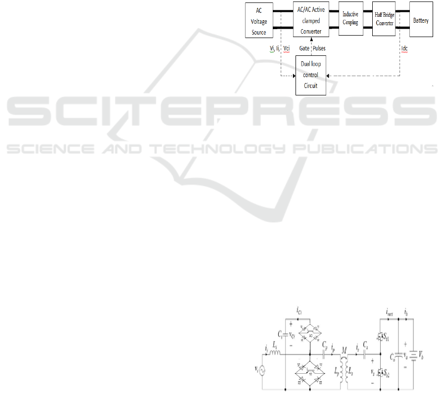
2 SYSTEM DESCRIPTION
The block diagram of the proposed system is shown
below in Fig 1.
Fig 1: Proposed system Block diagram.
To power the battery in this, an ac supply is linked
to the suggested converter. The battery serves as the
load in this. The voltage is increased using the
Ac/Ac active clamped conversion device in
accordance with the load requirements, and the rate
of supply is changed to a high frequency so that
inductively coupled transfer of power is superior
with higher frequencies. The half bridge converter
receives the transmitted power and converts it from
ac to dc. To ensure an effortless charging process
and prevent a dual frequency fluctuation (100Hz), a
dual loop regulation is offered to adjust the mean
current at the pack's side. The addition of a dead-
beat controller enhances the system's overall
dynamic performance.
Fig 2: AC/AC Converter.
ISPES 2023 - International Conference on Intelligent and Sustainable Power and Energy Systems
60

The suggested AC/AC converter combines an HB
matrix converter and an AC/AC boost converter. The
AC/AC converter is set up using two switches
connected to diode bridges. The input current
rectification and recharging regulation procedures in
the suggested IPT system are accomplished by
regulating the main AC/AC converter's cycle duration
using dual loops of control. Both switches S1 and S2
function in positive as well as negative phases and are
complimentary to one another. The proportion of the
duration of the switch S1's on-time to the switching
phase is known as the duty cycle, which stands for
the AC/AC converter.
A high-frequency unipolar square wave voltage
(Vp), whose magnitude and direction fluctuate on the
clamped voltage (VCi), is the resultant voltage of an
instantaneous AC–AC active–clamped HB converter.
The SS compensating system is used because it is
straightforward, affordable, highly efficient, and
compensates for loads independently. The two main
resonant networks are set to the identical resonant
frequency, which is equivalent to the frequency of the
power electronic switch, so as to maximise the
electrical power deliver capabilities and reduce the
VA grade of the converter. The secondary component
of the network has a proactive HB rectifier, and both
switches that operate Ss1 and Ss2, function at fs with
a set duty period of 0.5.
The generated duty cycle of 0.5 at the secondary
voltage Vs. Remember that the higher switch Ss1's
on-time to switching duration is referred to as the
required period ds of the converter. Both the resonant
networks have been adjusted to the switching
frequency and the phase offset across vp and vs is
required to be held from 0 to 180 degrees in enable to
transmit energy between the grid and battery pack.
Where Lp and Ls are the self-inductances of the
primary and secondary coils, Cp and Cs are the
primary and secondary compensation capacitors, and
s = 2fs is the switching angular frequency.
The modes of operation of the proposed converter
is provided below:
Fig 3a: Proposed Converter.
Mode 1:
The switch S1 is turned ON in this mode. The L1 gets
charged by the input source. The Cp discharges and
provides energy to the inductor Lp. In secondary Ss1
is ON and the inductor Ls provides energy to the load
through Cs.
Fig 3b: Mode 1 of the Proposed Converter.
Mode 2:
The switch S1 is still turned ON in this mode and L1
gets charged by the input source along with Cp. In
secondary Ss1 is ON and the inductor Ls provides
energy to the load through Cs.
Fig 4: Mode 2 of the Proposed Converter.
Mode 3:
The switch S1 is OFF and S2 is turned ON in this
mode and L1 gets discharged and charges C1 along
with Cp. In secondary Ss1 is ON and the inductor Ls
provides energy to the load through Cs.
Fig 5: Mode 3 of the Proposed Converter.
Direct AC/AC Active-Clamped Converter Inductive Coupled With Half-Bridge Converter With Reduced Switches For Battery Charging
Applications
61
Mode 4:
The switch S1 is OFF and S2 is turned ON in this
mode and L1 gets disconnected as it completely
discharged and C1 starts discharging and charges the
Cp. In secondary Ss1 is ON and the inductor Ls
provides energy to the load through Cs.
Fig 6: Mode 4 of the Proposed Converter.
Mode 5:
The switch S1 is OFF and S2 is turned ON in this
mode and L1 gets disconnected as it completely
discharged and C1 starts discharging and charges the
Cp. In secondary Ss2 is ON and the inductor Ls is
getting charged from Cs.
Fig 7: Mode 5 of the Proposed Converter.
Mode 6:
The switch S1 is OFF and S2 is turned ON in this
mode and L1 gets disconnected as it completely
discharged and C1 gets charged by the Cp. In
secondary Ss1 is ON and the inductor Ls is getting
discharged through Cs.
Fig 8: Mode 6 of the Proposed Converter.
For negative half cycle, the same process is repeated.
Fig 9: Mode 7 of the Proposed Converter.
Mode 7:
The switch S1 is turned ON in this mode. The L1 gets
charged by the input source in reverse direction. The
Cp discharges and provides energy to the inductor Lp.
In secondary Ss1 is ON and the inductor Ls provides
energy to the load through Cs.
Fig 10: Mode 8 of the Proposed Converter.
Mode 8:
The switch S1 is still turned ON in this mode and L1
gets charged by the input source along with Cp in
reverse direction. In secondary Ss1 is ON and the
inductor Ls provides energy to the load through Cs.
Fig 11: Mode 9 of the Proposed Converter.
ISPES 2023 - International Conference on Intelligent and Sustainable Power and Energy Systems
62
Mode 9:
The switch S1 is OFF and S2 is turned ON in this
mode and L1 gets discharged along with C1 and
charges Cp. In secondary Ss1 is ON and the inductor
Ls provides energy to the load through Cs.
Fig 12: Mode 10of the Proposed Converter.
Mode 10:
The switch S1 is OFF and S2 is turned ON in this
mode and L1 gets disconnected as it completely
discharged and C1 starts discharging along with Lp
and charges the Cp. In secondary Ss2 is ON and the
inductor Ls getting charged from Cs.
Fig 13: Mode 11 of the Proposed Converter.
Mode 11:
The switch S1 is OFF and S2 is turned ON in this
mode and L1 gets disconnected as it completely
discharged and C1 starts discharging along with Lp
and charges the Cp. In secondary Ss1 is ON and the
energy in inductor Ls is discharged to load through
Cs.
Fig 14: Mode 12 of the Proposed Converter.
Mode 12:
The switch S1 is OFF and S2 is turned ON in this
mode and L1 gets disconnected as it completely
discharged and C1 starts charging along with Lp from
Cp. In secondary Ss1 is ON and the energy in inductor
Ls is discharged to load through Cs.
A duty ratio is calculated to reduce the peak value of
the capacitor clamping voltage for the peak source
voltage is provided below
The source ripple current, Im, for peak source
voltage is provided below
The M is derived for peak value of source current in
which dp = Dpm, ii = Im, and ds = 0.5.
The supply side and load side compensation
capacitors are calculated as shown below:
The clamping capacitor at the supply side, Ci, is
determined according to the permissible ripple
voltage Vc is as shown below.
DUAL CONTROL MODULATION SCHEME.
The suggested linear AC/AC converter operates by
two control loops in order to attain unity source power
factor and modulate power output within the single
conversion phase.
Direct AC/AC Active-Clamped Converter Inductive Coupled With Half-Bridge Converter With Reduced Switches For Battery Charging
Applications
63
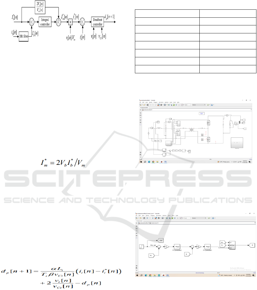
Fig 15: Dual Control Modulation Scheme.
To control the mean battery current across a line
cycle, an external loop is set up. An IIR filter may be
used to determine the mean current from the battery.
The maximum current source reference Im* from the
external control circuit is increased by vi/Vm to
provide the sine wave standard current Ii* used in the
internal current circuit.
The external current regulation loop, which
regulates the mean current through the battery during
a line cycle, generates the highest possible current
source reference Im*. Considering the average power
equilibrium at both ends of the circuit and the
presumption that energy losses were ignorable, the
maximum current supply reference Im* may be
roughly calculated.
where Ib* is the mean value of reference battery
current.
In order to achieve a unity power factor for the
instantaneous AC/AC converter input, the internal
control circuit is used to adjust the current source after
the grid voltage. The PDB controller is used in this
loop to regulate the mean switched source current.
The PWM signals powering the instantaneous
AC/AC converter are produced using the dual-
edge/triangle regulation. By synchronising the
sample at the maximum or trough for the carrier
signal that is used with a particular PWM generating
approach, the mean of the current source may be
determined. The deadbeat regulator produces the
following duty cycle:
3 SIMULATION RESULTS
The simulation parameters of the proposed system are
provided in the table given below:
Table 1.
Input Voltage
120 V
Input power
1 KW
Switching Frequency
85 KHZ
Inductor
1mH
Resonant Capacitor
11.86nF
Decoupling Capacitor
3.3mH
Output Capacitor
0.7mF
Load Resistance
62.5Ω
The simulation circuit for the proposed converter
is provided below:
Fig 16: Simulation circuit for the proposed converter.
In this, the supply voltage of 120V is applied to
the proposed converter and the load voltage reference
is varied from 100V to 250 V at t=0.1s. The
simulation circuit of the controller is provided below:
Fig 17: Simulation circuit for the proposed controller.
In this the load voltage and current is provided to
the voltage control loop and current control loop
respectively. The input voltage and decoupling
capacitor voltage is provided to the dead beat control
along with the reference current and from that duty
ratio is calculated. The obtained duty ratio is provided
to the pwm pulse generation and the generated pulses
are provided to the controller.
The load voltage and current is provided is
provided below:
ISPES 2023 - International Conference on Intelligent and Sustainable Power and Energy Systems
64
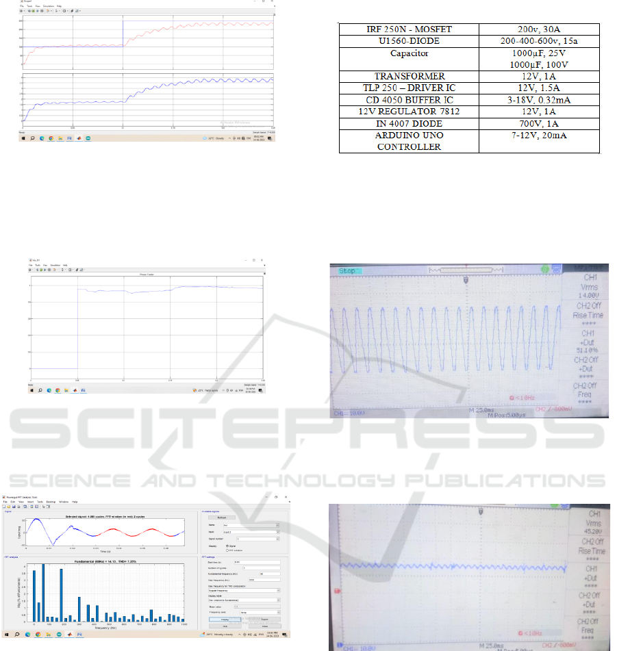
Fig 18: Load voltage and current.
In this, the reference voltage is varied from 100V to
220V at t=0.1s and the measured voltage follows the
reference voltage along with the current. The power
factor measured is provided below:
Fig 19: Power factor of the converter.
The power factor of the proposed converter is
around 0.94. The %THD of the supply current is
provided below:
Fig 20: THD for the proposed converter.
The %THD of the supply current is around 7.23%.
A hardware prototype model of proposed
converter with input voltage of 12V, 50 Hz is
developed with 48V as output voltage with load
resistance of 100 ohm. The hardware parameters is
provided below in the following Table II.
Table 2: Hardware Parameters.
Arduino uno control is used for generating the
pulses for the proposed inverter and it is provided to
driver circuit (TLP 250) in order to drive the mosfets
IRF 250. The input voltage waveform is provided
below:
Fig 21: Input voltage for the proposed converter.
The input voltage is around 14V. The load voltage
waveforms is provided below:
Fig 23: Load voltage proposed converter.
The load voltage is around 45.2V with voltage
division as 10V/div.
4 CONCLUSION
In this paper, a AC/AC active clamped converter
based battery charging system is presented along with
operational analysis design and control structure.
Additionally, a novel predictive dead-beat grid
Direct AC/AC Active-Clamped Converter Inductive Coupled With Half-Bridge Converter With Reduced Switches For Battery Charging
Applications
65

current control method and the linear mean current
charging were designed for the proposed converter,
improving the power factor. The power factor is
measured as 0.94 and %thd of the supply current is
around 7.23%. A hardware prototype model is
developed to verify the operation of the proposed
converter.
REFERENCES
Ramezani, A., Farhangi, S., Iman-Eini, H., Farhangi, B.,
Rahimi, R., & Moradi, G. R. (2019). Optimized LCC-
Series Compensated Resonant Network for Stationary
Wireless EV Chargers. IEEE Transactions on
Industrial Electronics, 66(4), 2756–2765.
Liu, J., Chan, K., Chung, C. Y., Hon, N., Liu, M., & Xu, W.
(2018). Single-Stage Wireless-Power-Transfer
Resonant Converter With Boost Bridgeless Power-
Factor-Correction Rectifier. IEEE Transactions on
Industrial Electronics, 65(3), 2145–2155.
Samanta, S., & Rathore, A. K. (2019). Small-Signal
Modeling and Closed-Loop Control of a Parallel–
Series/Series Resonant Converter for Wireless
Inductive Power Transfer. IEEE Transactions on
Industrial Electronics, 66(1), 172–182.
https://doi.org/10.1109/tie.2018.2823682
Samanta, S., & Rathore, A. K. (2018). A New Inductive
Power Transfer Topology Using Direct AC–AC
Converter With Active Source Current
Waveshaping. IEEE Transactions on Power
Electronics, 33(7), 5565–5577.
Phuoc Sang Huynh, & Williamson, S. S. (2019). Analysis
and Design of Soft-Switching Active-Clamping Half-
Bridge Boost Inverter for Inductive Wireless Charging
Applications. IEEE Transactions on Transportation
Electrification, 5(4), 1027–1039.
https://doi.org/10.1109/tte.2019.2930199
Moghaddami, M., & Sarwat, A. I. (2018). Single-Phase
Soft-Switched AC–AC Matrix Converter With Power
Controller for Bidirectional Inductive Power Transfer
Systems. IEEE Transactions on Industry
Applications, 54(4), 3760–3770.
Huynh, Phuoc Sang & Ronanki, Deepak & Vincent, Deepa
& Williamson, Sheldon. (2020). Overview and
Comparative Assessment of Single-Phase Power
Converter Topologies of Inductive Wireless Charging
Systems. Energies. 13. 2150. 10.3390/en13092150.
Yao, Yousu & Wang, Yijie & Liu, Xiaosheng & Lin,
Fanfan & Xu, Dian. (2017). A Novel Parameter Tuning
Method for Double-sided LCL Compensated WPT
System with Better Comprehensive Performance. IEEE
Transactions on Power Electronics. PP. 1-1.
10.1109/TPEL.2017.2778255.
Vu, V.-B., Phan, V.-T., Dahidah, M., & Pickert, V. (2019).
Multiple Output Inductive Charger for Electric
Vehicles. IEEE Transactions on Power
Electronics, 34(8), 7350–7368.
Charthad, Jayant & Chang, Ting & Liu, Zhaokai & Sawaby,
Ahmed & Weber, Marcus & Baker, Sam & Gore,
Felicity & Felt, Steve & Arbabian, Amin. (2018). A
mm-Sized Wireless Implantable Device for Electrical
Stimulation of Peripheral Nerves. IEEE Transactions
on Biomedical Circuits and Systems. PP. 1-14.
10.1109/TBCAS.2018.2799623.
ISPES 2023 - International Conference on Intelligent and Sustainable Power and Energy Systems
66
