
Design of Multilevel Inverter with Unbalanced Voltage Sources with
Reduced Number of Mosfets
SHRUTI
1 a
and
M. S. ASPALLI
1 b
Department of Electrical and Electronics Engineering (Affiliated to VTU Belgaum)
Poojya Doddappa Appa College of Engineering, Kalaburagi (Affiliated to VTU Belgaum),Karnataka, India
Keywords: Multilevel Inverter, Less Number of Switches, Unbalanced Voltage Sources, Total Harmonic Distortion,
Reduced Number of Switches.
Abstract: A pulse amplitude modulation template for Cascaded bridge driver this paper introduces a multilevel inverter.
A modulating waveform that is sinusoidal altered to fitting a single trigon bearer signal coverage by the
established power concept, which creates suitable template modifications for Cascaded-H-Bridge inverters.
Without further control adjustment, the CHB inverters can be used with these templates of any degree. The
suggested modulation resulted in nearly equal switching pulse distribution, equal allocation of the entire real
power between the switches that made up the system, and improves output voltage quality. The simulation is
done in MATLAB/Simulink software. A hardware representation is expand for the preferred 25 level inverter
and the of the inverter’s operation is verified.
1 INTRODUCTION
A multiple-level inverter development has been well
received lately for a range towards medium, low and
high-power applications. As a outcome of MLI is
skilled at producing a sinusoidal-like output by
combining switch and dc sources. The extra parts
utilised in the multiple-level inverter to provide
structural resilient include diodes and capacitors. To
enhance the quality of the power, efficiency, and
reliability, MLIs are utilised in assortment of
applications, such as solar energy systems, electric
cars, friction motors, etc.
In comparison to standard two-level inverters,
multilevel inverters may create high-quality output
with less switching, which reduces voltage stress,
electromagnetic interference, switching loss, etc.
Scientific interest was stimulated to multilayer
inverters for many uses, applications, including trains,
aircrafts, being their proficiency in resolving the
problems (Bana, P et al., R,2020). In late years, there
obsolete a lot of work done to further improve the
traditional multilevel inverter topologies that they are
more applicable for lowering losses and costs in light
of various applications.
a
https://orcid.org/0009-0003-3029-330X
b
https://orcid.org/0000-0002-5483-6415
The sequential arrangement of Mosfets, each of
the NPCMLI and FCMLI are prone to voltage balance
issues and module collapse. Apart from, CMLI is
clamping diodes or capacitors (Khoun Jahan et
al.,2019). However, the need for several
semiconductor devices to generate greater levels of
voltage at the result of these MLIs continues being
challenge. CMLI may be operated with equal
(symmetric), unequal (asymmetric), and variable dc
sources depending on the need and application.
While asymmetrical designs can raise voltage
levels with fewer dc sources, symmetrical MLIs are
easier to regulate. The suggested circuit's extra benefit
is the integration of a floating capacitor, which raises
the voltage level. Only the first voltage step's voltage
spike caused by inductive loads can be removed by
adding another switch. PV systems can use the MLI
that has been described.
Similar to the traditional CMLI, the circuit needs
several input sources. The constructions previously
mentioned incorporate an intermediate H-bridge for
producing the negative levels(Kaibalya Prasad Panda
et al.,2020). Potential non-boosting constructions that
greatly lower pressure are presented, excluding the
whole bridge. In addition, there was a major increase
in interest in lately in developing SC MLIs with built-
in boosting capability. The SC MLIs are appropriate
for a high-frequency ac distribution of power and
84
SHRUTI, . and ASPALLI, M.
Design Of Multilevel Inverter with Unbalanced Voltage Sources with Reduced Number of Mosfets.
DOI: 10.5220/0012508800003808
Paper published under CC license (CC BY-NC-ND 4.0)
In Proceedings of the 1st International Conference on Intelligent and Sustainable Power and Energy Systems (ISPES 2023), pages 84-92
ISBN: 978-989-758-689-7
Proceedings Copyright © 2024 by SCITEPRESS – Science and Technology Publications, Lda.

balancing the SC voltages with no use of auxiliary
sensors or extra inductors or transformers (Sze Sing
Lee,2020).
The multilevel inverter topography that are given
make use of the same fundamental unit to build
higher levels of resultant voltages with a reduced
number of parts (Roy, Tet al.,2021). A two-step, twofold
boosted output may be produced using the
fundamental unit, which consists of a one dc supply
and one capacitor. Self-voltage balancing is made
possible by charging a capacitor in aligned while carry
out it in sequence with the origin. These circuits
require extra dc sources for single-phase expansion. In
the contrast hand, by using the multilevel inverter in
both symmetrical and asymmetrical modes, this
presents a chance to raise the levels of voltage (17-
level, 25-level, 49-level, and 81-level) (Lin et
al.,2020).
In recent years, several pulse width modulation
strategy have been created with the primary goal of
regulating voltage quality by producing the proper
switching pulse (Lee et al.,2020).
The development of switched capacitor-multi-
level inverters using a one input, extend style, is a
current research topic. As a result, this architecture is
ineffective in raising the voltage. The suggested MLI
circuits satisfactorily lower the electrical stress that
damages a enormous of circuit parts.
Additionally, research is being done to create a
single-dc composite NMLI-based structure that would
produce output at 7 levels, 9 levels, and 11 levels
while putting less strain on the Mosfets. However, the
11-level inverter's voltage gain is restricted to a
maximum of 2.5 times the source voltage. Recent MLI
configurations use fewer components to achieve
significant voltage gain (six, four, and three times,
respectively) (Kaibalya Prasad Panda,2020). To
produce the ac voltage output in these circuits, a
traditional H-bridge is not necessary (Panda et
al.,2020).
A new multilevel inverter with asymmetrical
sources of voltage ratio 1:2:4:6 is directed to obtain 25
voltage levels without increasing the quantity of
Mosfets. The maximum voltage value is of two times
of V
4
which provides the highest charge among the
input charge sources. switching table is provided and
the proposed inverter’s modes of operation are
analysed.
2 SYSTEM EXPLANATION
The present inverter is given below in Figure 1. In this,
four dc sources are attached to the proposed multi
level inverter and the ratio of dc voltage sources is
1:2:4:6. The gate pulses for the inverter Mosfets are
provided from the switching circuit as maintained by
the switching table. The proposed 25-level MLI
circuit is comprised of 12 power electronic Mosfets
(MS1–MS12), single diode (D1), and four dc voltage
sources (V1-V4). The circuit produces a 25-level
output voltage (0, ±Vdc, ±2Vdc, ±3Vdc,…, ±12Vdc)
eliminating H-bridge for the inversion of polarity.
Voltage ratio between the sources Voltage 1, Voltage
2, Voltage 3 and Voltage 4 are (V1:V2:V3:V4) is
provided at 1:2:4:6 in the steady state.
Figure 1: Block diagram.
Following is Fig 2, which shows proposed 25-level
inverter:
Figure 2: Proposed 25 level multi-level inverter.
The switching table of the multilevel inverter is
provided in the table 1 as follows:
Table 1.
M
S
1
M
S
2
M
S
3
M
S
4
M
S
5
M
S
6
M
S
7
M
S
8
M
S
9
M
S
10
M
S
11
M
S
12
V
o
Design Of Multilevel Inverter with Unbalanced Voltage Sources with Reduced Number of Mosfets
85

O
N
O
N
O
N
O
N
V
d
c
O
N
O
N
O
N
O
N
O
N
2
V
d
c
O
N
O
N
O
N
O
N
O
N
3
V
d
c
O
N
O
N
O
N
O
N
O
N
4
V
d
c
O
N
O
N
O
N
O
N
O
N
5
V
d
c
O
N
O
N
O
N
O
N
6
V
d
c
O
N
O
N
O
N
O
N
7
V
d
c
O
N
O
N
O
N
O
N
O
N
8
V
d
c
O
N
O
N
O
N
O
N
O
N
9
V
d
c
O
N
O
N
O
N
O
N
O
N
1
0
V
d
c
O
N
O
N
O
N
O
N
O
N
1
1
V
d
c
O
N
O
N
O
N
O
N
O
N
O
N
1
2
V
d
c
-
-
-
-
-
-
-
-
-
-
-
-
Z
er
o
O
N
O
N
O
N
O
N
O
N
O
N
-
1
V
d
c
O
N
O
N
O
N
O
N
O
N
O
N
-
2
V
d
c
O
N
O
N
O
N
O
N
-
3
V
d
c
O
N
O
N
O
N
O
N
-
4
V
d
c
O
N
O
N
O
N
O
N
O
N
-
5
V
d
c
O
N
O
N
O
N
O
N
O
N
-
6
V
d
c
O
N
O
N
O
N
O
N
O
N
O
N
-
7
V
d
c
O
N
O
N
O
N
O
N
O
N
O
N
-
8
V
d
c
O
N
O
N
O
N
O
N
-
9
V
d
c
O
N
O
N
O
N
O
N
-
1
0
V
d
c
O
N
O
N
O
N
O
N
O
N
-
1
1
V
d
c
O
N
O
N
O
N
O
N
O
N
-
1
2
V
d
c
ISPES 2023 - International Conference on Intelligent and Sustainable Power and Energy Systems
86

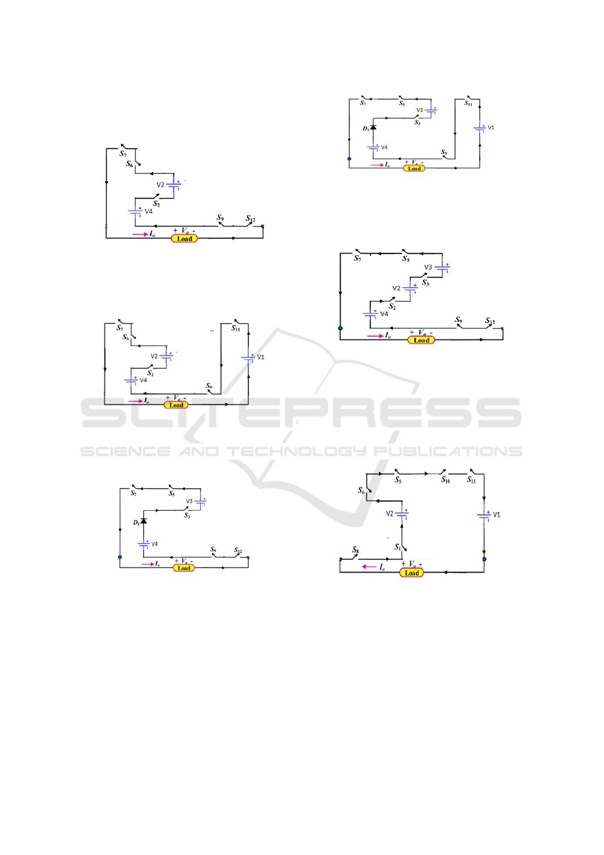
Mode 1:
The Mosfets MS
5
, MS
7
, MS
10
and MS
11
are operating.
The output voltage is around Vdc (12V). The
operational circuit for mode 1 operation is provided
below:
Figure 2(a): mode 1 circuit of 25 multi-level inverter.
Mode 2:
The Mosfets MS
1
,MS
6
,MS
7
,MS
9
and MS
12
are
operating. The output voltage is 2Vdc (24V).
Figure 2(b): mode 2 circuit of 25 multi-level inverter.
Mode 3:
The Mosfets MS
1
, MS
6
, MS
7
, MS
9
and MS
11
are
operating. The output voltage is 3Vdc (36V).
Figure 2(c): mode 3 circuit of 25 multi-level inverter.
Mode 4:
The Mosfets MS
4
, MS
5
, MS
7
, MS
9
and MS
12
are
operating. The output voltage is 4Vdc (48V).
Figure 2(d): mode 4 circuit of 25 multi-level inverter.
Mode 5:
The Mosfets MS
4
, MS
5
, MS
7
, MS
9
and MS
11
are
operating. The output voltage is 5Vdc (60V).
Figure 2(e): mode 5 circuit of 25 multi-level inverter.
Mode 6:
The Mosfets MS
6
, MS
7
, MS
9
and MS
12
are operating.
The output voltage is 6Vdc (72V).
Figure 2(f): mode 6 circuit of 25 multi-level inverter.
Mode 7:
The Mosfets MS
6
, MS
7
, MS
9
and MS
11
are operating.
The output voltage is 7Vdc (84V).
Figure 2(g): mode 7 circuit of 25 multi-level inverter.
Design Of Multilevel Inverter with Unbalanced Voltage Sources with Reduced Number of Mosfets
87
Mode 8:
The Mosfets MS
2
, MS
6
, MS
7
, MS
9
and MS
12
are
operating. The output voltage is 8Vdc (96V).
Figure 2(h): mode 8 circuit of 25 multi-level inverter
Mode 9:
The Mosfets MS
2
, MS
6
, MS
7
, MS
9
and MS
11
are
operating. The output voltage is 9Vdc (108V).
Figure 2(i): mode 9 circuit of 25 multi-level inverter.
Mode 10:
The Mosfets MS
3
, MS
5
, MS
7
, MS
9
and MS
12
are
operating. The output voltage is 10Vdc (120V).
Figure 2(j): mode 10 circuit of 25 multi-level inverter.
Mode 11:
The Mosfets MS
3
, MS
5
, MS
7
, MS
9
and MS
11
are
operating. The output voltage is 11Vdc (132V).
Figure 2(k): mode 11 circuit of 25 multi-level inverter.
Mode 12:
The Mosfets MS
2
, MS
3
, MS
5
, MS
7
, MS
9
and MS
12
are
operating. The output voltage is 12Vdc (144V).
Figure 2(l): mode 12 circuit of 25 multi-level inverter.
Mode 13:
In this mode all the Mosfets are turned OFF. The
output voltage is around 0V.
Mode 14:
The Mosfets MS
1
, MS
5
, MS
6
, MS
8
, MS
10
and MS
11
are
operating. The output voltage is -Vdc (-12V).
Figure 2(m): mode 14 circuit of 25 multi-level inverter.
\Mode 15:
The Mosfets MS
1
, MS
5
, MS
6
, MS
8
, MS
10
and MS
12
are
operating. The output voltage is -2Vdc (-24V).
ISPES 2023 - International Conference on Intelligent and Sustainable Power and Energy Systems
88

Figure 2(n): mode 15 circuit of 25 multi-level inverter.
Mode 16:
The Mosfets MS
4
, MS
8
, MS
10
and MS
11
are operating.
The output voltage is -3Vdc (-36V).
Figure 2(o): mode 16 circuit of 25 multi-level inverter.
Mode 17:
The Mosfets MS
4
, MS
8
, MS
10
and MS
12
are operating.
The output voltage is -4Vdc (-48V).
Figure 2(p): mode 17 circuit of 25 multi-level inverter.
Mode 18:
The Mosfets MS
5
, MS
6
, MS
8
, MS
10
and MS
11
are
operating. The output voltage is -5Vdc (-60V).
Figure 2(q): mode 18 circuit of 25 multi- level inverter.
Mode 19:
The Mosfets MS
5
, MS
6
, MS
8
, MS
10
and MS
12
are
operating. The output voltage is -6Vdc (-72V).
Figure 2(r): mode 19 circuit of 25 multi-level inverter.
Mode 20:
The Mosfets MS
2
, MS
5
, MS
6
, MS
8
, MS
10
and MS
11
are
operating. The output voltage is -7Vdc (-84V).
Figure 2(s): mode 20 circuit of 25 multi-level inverter.
Mode 21:
The Mosfets MS
2
, MS
5
, MS
6
, MS
8
, MS
10
and MS
12
are
operating. The output voltage is -8Vdc (-96V).
Figure 2(t): mode 21 circuit of 25 multi-level inverter.
Mode 22:
The Mosfets MS
3
, MS
8
, MS
10
and MS
11
are operating.
The output voltage is around -9Vdc (-108V). The
operational circuit for mode 22 operation is provided
below:
Figure 2 (u): mode 22 circuit of 25 multi-level inverter.
Design Of Multilevel Inverter with Unbalanced Voltage Sources with Reduced Number of Mosfets
89

Mode 23:
The Mosfets MS
3
, MS
8
, MS
10
and MS
12
are operating.
The output voltage is -10Vdc (-120V).
Figure 2 (v): mode 23 circuit of 25 multi-level inverter.
Mode 24:
The Mosfets MS
2
, MS
3
, MS
8
, MS
10
and MS
11
are
operating. The output voltage is -11Vdc (-132V).
Figure 2 (w): mode 24 circuit of 25 multi-level inverter.
Mode 25:
The MS
2
, MS
3
, MS
8
, MS10 and MS
12
are operating.
The output voltage is around -12Vdc (-144V). The
operational circuit for mode 25 operation is provided
below:
Figure 2(x): mode 25 circuit of 25 multi-level inverter.
3 SIMULATION FORMAT &
OUTCOME
The simulation variables for the preferred inverter are
provided that below in Table 2:
Table 2: Simulation variables.
Input Voltage
156 V
Frequency
50 HZ
Load power
200W
Load Resistance
100 ohm
The simulation circuit of the 25 multi-level
inverter is provided that below in Figure 3.
Figure 3: Simulation circuit of 25 multi-level inverter.
It includes 12 power electronic Mosfets and 4
voltage sources of the amplitude ratio of 1:2:4:6 with
load of 100Ω. Load voltage is provided below in
Figure 4.
Figure 4: output voltage of 25 level inverter.
The amplitude of load voltage is in the range of
144V to -144V with each level is of 12V. In this there
ISPES 2023 - International Conference on Intelligent and Sustainable Power and Energy Systems
90

are 12 positive voltage levels and 12 negative voltage
levels and with zero level, we got 25 level voltage.
The %THD for the generated voltage of the present
inverter is provided below in Fig 5.
Figure 5: %THD of load voltage of 25 multi-level inverter.
Table 3: Hardware Parameters.
IRF 250N – MOSFET
200V, 30A
U1560 - DIODE
200-400-600V, 15a
Capacitor
1000 µF, 25V
TRANSFORMER
12V, 1A
TLP 250 – DRIVER IC
12V, 1.5A
CD 4050 BUFFER IC
3-18V, 0.32mA
12V REGULATOR 7812
12V, 1A
IN 4007 DIODE
700V, 1A
ARDUINO UNO
CONTROLLER
7-12V, 20mA
Arduino uno control utilised for give rise to the
pulses for the preferred inverter also, it is provided to
driver circuit (TLP 250) in aiming to operate the
mosfets IRF 250. The single-phase inverter with 25
levels voltage is provided below:
Figure 6: In positive cycle, twelve levels and in negative
cycle twelve levels and with zero level we get twenty-five
levels in the above waveform.
Figure 7: Hardware setup of proposed system.
4 CONCLUSIONS
A new multi-level inverter with 25 levels and
unbalanced voltage sources in the ratio 1:2:4:6 is
designed in this. To achieve the needed voltage levels,
a switching pattern is developed, and the proposed
inverter's operation is carefully examined. When
compared to traditional mli topologies, the simulation
work is done and the preferred output voltage is
obtained with fewer Switches. The proposed inverter's
% THD reduction is assessed at less than 4%. The
advantages and applications of this proposed
converter is four switches operates under lower
frequencies and hence losses are reduced. More than
50% of switches operates below frequency;
consequently, switching loss is reduced and usable in
EVs where multiple batteries are used compared to the
literature. The higher voltage battery supplies the load
along with charging the low voltage batteries.
REFERENCES
https://doi.org/10.1109/pesgre45664.2020.90705
Sze Sing Lee, Lee, K.-B., Ibrahim Mohd Alsofyani, Bak,
Y., & Jing Fang Wong. (2019). Improved
Switched-Capacitor Integrated Multilevel
Inverter With a DC Source String. IEEE
Transactions on Industry Applications, 55(6),
7368–7376.
https://doi.org/10.1109/tia.2019.2893850
Roy, T., & Pradip Kumar Sadhu. (2021). A Step-Up
Multilevel Inverter Topology Using Novel
Design Of Multilevel Inverter with Unbalanced Voltage Sources with Reduced Number of Mosfets
91

Switched Capacitor Converters With Reduced
Components. IEEE Transactions on Industrial
Electronics, 68(1), 236–247.
https://doi.org/10.1109/tie.2020.2965458
Lin, W., Zeng, J., Liu, J., Yan, Z., & Hu, R. (2020).
Generalized Symmetrical Step-Up Multilevel
Inverter Using Crisscross Capacitor Units. IEEE
Transactions on Industrial Electronics, 67(9),
7439–7450.
https://doi.org/10.1109/tie.2019.2942554
Lee, S. S., Lim, C. S., & Lee, K.-B. (2020). Novel Active-
Neutral-Point-Clamped Inverters With Improved
Voltage-Boosting Capability. IEEE Transactions
on Power Electronics, 35(6), 5978–5986.
https://doi.org/10.1109/tpel.2019.2951382
Kaibalya Prasad Panda, Prabhat Ranjan Bana, & Panda, G.
(2020). A Switched-Capacitor Self-Balanced
High-Gain Multilevel Inverter Employing a
Single DC Source. IEEE Transactions on
Circuits and Systems Ii-Express Briefs, 67(12),
3192–3196.
https://doi.org/10.1109/tcsii.2020.2975299
ISPES 2023 - International Conference on Intelligent and Sustainable Power and Energy Systems
92
