
Design of Three Phase Nine Level Cascaded H-Bridge Multilevel
Inverter with Low Total Harmonic Distortion Based Pulse-Width
Modulation Method
Pooja B Dandoti
1
a
, M.S.Aspalli
2
b
Department of Electrical and Electronics Engineering, Poojya Doddappa Appa College of Engineering Kalaburagi,
Karnataka, India
Keywords: Multi level inverters, Cascaded H-Bridge MLI, Three Phase inverters, Total Harmonic Distortion, Single
carrier modulation scheme.
Abstract: This paper proposes a three phase nine level CHBMLI with single carrier signal-based model. By modifying
a sine wave modulating waveform to fit inside a single triangle carrier signal range, the suggested control
approach produces sufficient modulating templates for CHB inverters. These templates don't require any
further control change and may be applied to CHB inverters of any level. With the suggested modulation, a
nearly uniform allocation of switching pulses, and equal distribution of the total actual power among the
power switches that make up the system, and improved quality of load voltage have been attained. The
simulation is to be carried out in MATLAB/Simulink software.
1
INTRODUCTION
Recent years have seen a noticeable improvement
in energy-conditioning network topologies and the
accompanying control/modulation techniques in the
study of power electronics. This advancement is
closely related to the global search for more
ecologically acceptable and renewable electricity
sources and uses. When it comes to power
electronics, dc-ac converters constitute some of the
crucial parts utilised in a variety of crucial
applications, such as extruders, rolling and grinding
mills, and compressors, to mention a few. Power
electronics inverters must have high voltages at the
inverter and a range of functional result power quality
indicators in order for this deployment to be
successful. The ideal device for meeting these needs
is the multilayer inverter, or MLI. According to
reports in the literature, the widespread use of
multilayer inverter designs is a result of knowledge of
MLIs' intrinsic potentials and their good effects on a
number of industrial applications(Charles Ikechukwu
odeh et al.,2021). The most popularly used
modulation scheme to control the amplitude and
a
https://orcid.org/ 0009-0002-9442-1449
b
https://orcid.org/0000-0002-5483-6415
frequency of the synthesized output voltage
waveform of CHB MLI is the triangular carrier- based
sinusoidal pulse width modulation. Inverter- phase-
leg is the basis for its approach to creating gating
signals. A single modulating parameter that differs is
the angle of phase shift, which clearly shows that the
identical control principle continues in every phase of
the inverter(Ahmed et al.,2020). In order to set the
zero-sequence signal to zero, the control concept
precisely compares a modulation signal with
fundamental frequency and high frequency carrier
signal. The expansion of SPWM to multilevel and/or
multiphase systems just requires multiple instances of
different SPWM pulse generation does not actually
entail any rigorous and sophisticated computing
challenges. The PS PWM asserts excellent
modulation performance with regard to switching
pulse distribution across the power switches used for
forming cascading modules. Numerous strategies
have been proposed for this combinational notion in
order to combine the good modulation qualities that
are built into IPD and PS PWM systems, as
illustrated. As previously indicated, a fundamental
need for the expansion of SPWM to an array of ouput
levels for the inverter per inverter phase-leg is the
variety of the carrier signals. In other words, a
generating triangle carrier is tagged to each of the
synthesised voltage levels of the inverter in an
B Dandoti, P. and Aspalli, M.
Design of Three Phase Nine Level Cascaded H-Bridge Multilevel Inverter with Low Total Harmonic Distortion Based Pulse-Width Modulation Method.
DOI: 10.5220/0012544900003808
Paper published under CC license (CC BY-NC-ND 4.0)
In Proceedings of the 1st International Conference on Intelligent and Sustainable Power and Energy Systems (ISPES 2023), pages 167-172
ISBN: 978-989-758-689-7
Proceedings Copyright © 2024 by SCITEPRESS – Science and Technology Publications, Lda.
167

inverter phase-leg. It is unavoidable that this inverter
arrangement will use a sizable quantity of carrier
waves regardless of the conventional LS or PS
SPWM scheme(S. K.Sahoo et al.,2018) .Furthermore,
accurate synchronisation between these multicarrier
signals is necessary for the CHB MLI system to
provide inverter parameter waveforms of high
quality. Sampling concerns, memory limitations, and
estimation delays provide challenges in attaining this
synchronisation and tend to have a detrimental impact
on the dynamical efficiency of digital controlled CHB
MLI. The features of this SPWM approach can be
summarised as follows: just a single carrier wave is
required involves straightforward computations,
leading to in computationally simpler systems;
uneven allocation of switching commands between
the devices resulting in switching devices and
different distributing of the all around inverter power
inverter among the CHB units(J.Ma et al.,2020). In
the management of CHB MLI, phase-shifted SPWM
outperformed in-phase level-shifted SPWM due to
these modulating characteristics. In this paper, a
stacked H-bridge multilevel inverter PWM template
is presented (Xiangjun et al,2018). Its stateal
approach, which modifies the sine modulating
waveform to fit in a single triangle carrier signal
range in order to provide the necessary inverter
waveform template for the MLI, is developed upon
the stateal concept of same-phase disposition level-
shifted SPWM. A straightforward reverse-voltage-
sorting algorithm efficiently eliminates the evident
inherent disadvantage of this in-phase , level-shifted
SPWM (non-distribution for switching inverters to
power switches and uneven inverter power sharing)
from the modulation scheme(C.Liu et al.,2020)( G.
Zhang et al.,2019). In practise, the suggested control
strategy creates an alternate modulation scheme that
bridges the gap between level- and phase-shifted
carrier-based SPWM approaches, inheriting the best
aspects of both modulation systems.
2
SYSTEM DESCRIPTION
The following circuit diagram presents the three
phase NINE level CHBMLI operated with single
carrier signal based pwm strategy.
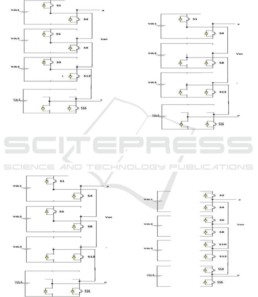
Figure 1: Three phase Cascaded H-Bridge Inverter
The DC voltage source is connected with the
inverter which provides three phase supply to load.
The voltage amplitude of each source is provided as
12V. The circuit configuration of phase A of nine
level cascaded H-Bridge MLI is provided below in
Fig. 2.
Figure 2: Circuit configuration of Phase A of Three phase
Cascaded H Bridge Inverter
As a result of multiplying its input voltage source,
Vdc, by nine, phase A of the nine-level CHB MLI has
produced nine steps of inverter, including 4Vin,
3Vdc, 2Vdc, Vdc, 0, -Vdc, -2Vdc, -3Vdc, and -4Vdc.
the ensuing AC voltage inverter will swing across
zero level from +4Vdc to -4Vdc. The status of each
semiconductor device's switch ON and switch OFF
state determines how MLI will operate. The outcome
generated by the inverter will depend on how the
switching state is configured. There are nine possible
configurations for the switching state on the nine level
CHB-MLI. Each configuration's inverter voltage may
be described as follows:
State 1:In this state the SWITCH1, SWITCH8,
SWITCH5, SWITCH4, SWITCH12, SWITCH9,
SWITCH13 and SWITCH16 are ON, therefore the inverter
voltage is 4 times of source voltage (negative polarity).
Figure 3: Operational circuit of State 1
ISPES 2023 - International Conference on Intelligent and Sustainable Power and Energy Systems
168
State 2: In this state the SWITCH1, SWITCH8,
SWITCH5, SWITCH4, SWITCH12, SWITCH9 and
SWITCH16 are ON, therefore the inverter voltage is
3 times of source voltage (negative polarity).
Figure 4: Operational circuit of State 2
State-3:In this state the SWITCH1, SWITCH8,
SWITCH5, SWITCH4, SWITCH12 and SWITCH16
are ON, therefore the inverter voltage is 2 time of
source voltage (negative polarity).
Figure 5: Operational circuit of State 3
State-4:In this state the SWITCH1, SWITCH8,
SWITCH4, SWITCH12 and SWITCH16 are ON,
therefore the inverter voltage is source voltage
(negative polarity).
Figure 6: Operational circuit of State 4
State-5:In this state the SWITCH2 SWITCH4,
SWITCH6 SWITCH8, SWITCH10, SWITCH12,
SWITCH14 and SWITCH16 are ON, therefore the
inverter voltage is 0.
Figure 7: Operational circuit of State 5
State 6:In this state when SWITCH2 SWITCH3,
SWITCH6, SWITCH7, SWITCH10, SWITCH11,
Design of Three Phase Nine Level Cascaded H-Bridge Multilevel Inverter with Low Total Harmonic Distortion Based Pulse-Width
Modulation Method
169

SWITCH14 and SWITCH15 are ON, therefore the
inverter voltage is four times of source voltage.
Figure 8: Operational circuit of State 6
State-7:In this state when SWITCH2 SWITCH3,
SWITCH6, SWITCH7, SWITCH10, SWITCH11
and SWITCH15 are ON, therefore the inverter
voltage is three times of source voltage.
Figure 9: Operational circuit of State 7
State-8: In this state when SWITCH2 SWITCH3,
SWITCH6, SWITCH7, SWITCH11 and SWITCH15
are ON, therefore the inverter voltage is 2 times of
source voltage.
Figure 10: Operational circuit of State 8
State-9:In this state when SWITCH2 SWITCH3,
SWITCH6, SWITCH11 and SWITCH15 are ON,
therefore the inverter voltage is source voltage
Figure 11: Operational circuit of State 9
ISPES 2023 - International Conference on Intelligent and Sustainable Power and Energy Systems
170
The phase B and C state principle is same as
phase A but the gate pulses are shifted or delayed for
phase B and C by 120 and 240 degrees respectively.
3
PWM Modulation strategy
In the proposed modulation system, the many
triangular carrier signals have been replaced by a
single carrier, which is an outgrowth of IPD level-
shifted SPWM. In order to properly stack the
synthesised pulses from any of the series H-bridges,
the continuous zones occupied by these multiple
carrier in the classic level-shifted SPWM must still
be present in this representation. More intriguing is
the fact that the deployed MWT is formed from a
phase- disposition level-shifted SPWM idea, despite
the CHB inverter system's ability to provide
identical power balancing among the constituent
units. It is important to recognise that modelling
such MWT with the required quantity of inverter
voltage levels just requires using information about
the CHB MLI setup that is already well-known
Figure 12: Single carrier based PWM modulation
strategy
4
SIMULATION SETUP
& RESULTS
The simulation parameters for the proposed
inverter are provided below in Table I:
TABLE 1. Simulation Parameter
The simulation circuit for the nine level
inverter is provided below:
Figure 13. Simulation circuit of 9 level CHBMLI
It consists of 4 dc voltage sources of 12V for
each phase as each source is connected to single
bridge which is connected in cascade structure to
get multi-level inverter voltage.
The Phase A voltage is of nine levels from 4Vdc
to -4Vdc. Similarly for phase B and Phase C but with
120- and 240-degree phase shifted respectively. The
voltage waveforms of the 9 level three phase multi
level inverter is provided below:
Figure 14. Three phase voltage waveform of
nine level CHBMLI
Input Voltage
48V
Input power
100W
Load Frequency
50 HZ
Load Resistance
100 ohm
Design of Three Phase Nine Level Cascaded H-Bridge Multilevel Inverter with Low Total Harmonic Distortion Based Pulse-Width
Modulation Method
171
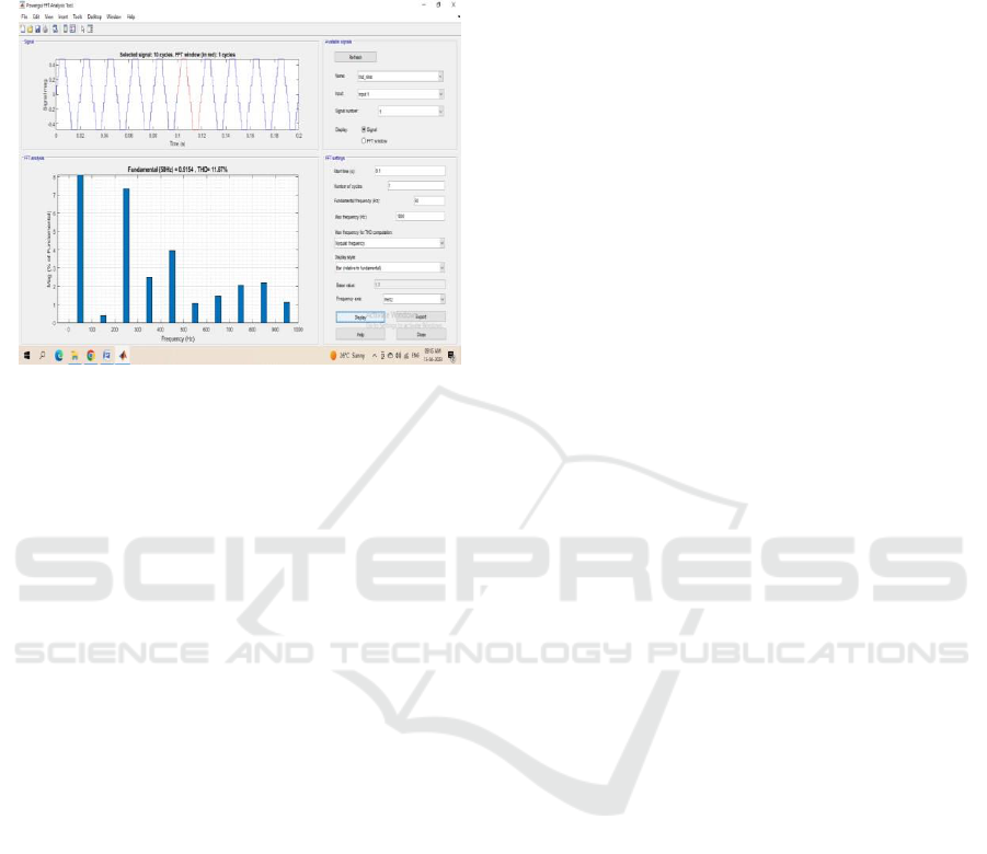
The voltage is varying from 48V to -48V with
voltage levels of 48V, 36V, 24V, 12V, 0, -12V, -24V,
-36V and -48V. The %THD of the inverter is
provided below
Figure 15: %THD of three phase MLI
REFERENCES
Charles Ikechukwu odeh, Arkadiusz Lewicki and Marcin
Morawiec “A Single-Carrier-Based Pulse-Width
Modulation Template for Cascaded H-Bridge
Multilevel Inverters” in IEEE Access, vol. 9, pp.
42182-42191, march 2021, doi :
10.1109/ACCESS.2021.3065743.
Odeh, C.I, Kondratenko, D, Lewicki, A, Morawiec, M,
Jąderko, A, Baran, J. Pulse-Width Modulation
Template for Five-Level Switch-Clamped H-
Bridge-Based Cascaded Multilevel
Inverter. Energies 2021, 14, 7726.
https://doi.org/10.3390/en14227726
S. K. Chattopadhyay and C. Chakraborty, ‘‘Full-bridge
converter with naturally balanced modular
cascaded H-bridge waveshapers for offshore
HVDC transmission,’’ IEEE Trans. Sustain.
Energy, vol. 11, no. 1, pp. 271–281, Jan. 2020, doi:
10.1109/TSTE.2018.2890575
Ahmed, M. S. Manoharan, and J.-H. Park, ‘‘An efficient
single-sourced asymmetrical cascaded multilevel
inverter with reduced leakage current suitable for
single phase PV systems “, IEEE Transactions,
Energy covers, vol. 34 no.1, pp 211-220, March
2019, doi: 10.1109/TEC.2018.2874076
S. K. Sahoo and T. Bhattacharya, "Phase- Shifted Carrier-
Based Synchronized Sinusoidal PWM Techniques
for a Cascaded H-Bridge Multilevel Inverter," in
IEEE Transactions on Power Electronics,vol.33,
no. 1, pp. 513-524,Jan. 2018, doi:
10.1109/TPEL.2017.2669084
J.Ma,X.Wang,F.Blaabjerg,W.Song,S.Wang and T. Liu,
‘‘Multisampling method for single-phase grid-
connected cascaded H-bridge inverters,’’ IEEE
Trans.Ind. Electron., vol. 67
, no. 10, pp. 8322–
8334, Oct. 2020, doi: 10.1109/TIE.2019.2947864.
Xiangjun Zeng, Deling Gong, Mi-lan Wei, Jing Xie,
“Research on novel hybrid multilevel inverter with
cascaded H-bridges at alternating current side for
high-voltage direct current transmission”, IET
Power Electronics, vol 11,no 12,p.1914-1925 Oct
2018
.
C. Liu, N. Gao, X. Cai, and R. Li, ‘‘Differentiation power
control of modules in second-life battery energy
storage system based on cascaded H-bridge
converter,’’ IEEE Trans. Power Electron., vol. 35,
no. 6, pp. 6609–6624, Jun. 2020, doi:
10.1109/TPEL.2019.2954577.
G. Zhang, Z. Tian, P. Tricoli, S. Hillmansen, Y. Wang, and
Z. Liu, ‘‘Inverter operating characteristics
optimization for DC traction power supply
systems,’’ IEEE Trans. Vehicle Technol., vol. 68,
no. 4, pp. 3400–3410, Apr. 2019, doi:
10.1109/TVT.2019.2899165
J. Ma, X. Wang, F. Blaabjerg, W. Song, S. Wang, and T.
Liu, ‘‘Realtime calculation method for Single-
Phase Cascaded H-bridge Inverters Based on
Phase-Shifted Carrier Pulse Width Modulation,’’
IEEE Trans.Power Electron., vol. 35,
no. 1,pp.977
987,Jan.2020, doi:10.1109/TPEL.2019.291422
ISPES 2023 - International Conference on Intelligent and Sustainable Power and Energy Systems
172
