
IMPLEMENTATION OF A DEVICE COMPATIBLE WITH
DIFFERENT FIELDBUSES USING RECONFIGURABLE
CIRCUITS
Miguel Ángel Domínguez, Mª Dolores Valdés, Mª José Moure
Department of Electronic Technology, University of Vigo, Vigo, Galicia, Spain
Keywords: Industrial networks, Fieldbuses, WorldFIP, Profibus, FPGA
Abstract: Fieldbuses are serial communication networks very used in industrial control applications. They constitute
the lower level of the communication networks in a flexible manufacturing system. Nowadays there are a
lack of standardization in the area of fieldbuses and it supposes the existence of a lot of proprietary
protocols. Thus, the interconnection of equipment from different manufacturers has become very
problematic. It implies that a change in equipment supposes a change in the fieldbus too with the
consequent economic losses. This paper proposes the implementation of a device using reconfigurable
circuits such as FPGAs (Field Programmable Gate Arrays) that can be used as a communication processor,
compatible with different fieldbuses making only little changes in the programming code and in the level
and impedance matching circuit (depending on the electrical features of the corresponding fieldbus). Thus,
the same hardware can be connected to different fieldbuses. The implementation of fieldbus communication
processors using FPGAs implies that the interface can be easily adapted to different protocols (improvement
in the interconnection between products of different manufacturers) and that the programming code can be
easily modified, adding new functionality when it is necessary.
1 INTRODUCTION
According to the definition of the IEC (International
Electrotechnical Commision) and the ISA
(Instrument Society of America), fieldbuses are
digital serial, multidrop data buses for low-level
communication of industrial control process and
instrumentation devices like actuators, sensors and
local controllers. The aim of fieldbuses is the serial
communication between primary elements of
automation (sensors and actuators with control and
measurement functions) and control devices of a
higher level (PLCs, numeric control machines,
processors, etc.).
Before the appearance of fieldbuses, the
connections between process units (PLCs,
controllers, etc.) and field devices (sensors and
actuators) were point-to-point links. It meant
complex (a lot of wires) and expensive (in time and
money) installations. Also the maintenance and
modification tasks were harder. These problems are
solved with fieldbuses because all devices are
connected through a single physical medium
(twisted pair, coaxial, two wires, optical fiber, etc.)
extended over the whole area of the distributed
control process system (cost reduction). Thus, new
devices can be added, connecting to the fieldbus,
without additional wiring (easy maintenance and
modification).
It can be said that fieldbuses emerged as a
response to the following needs: wiring reduction in
installations, easily reconfigurable systems, reduced
transmission times, data transmission reliability,
intrinsic security in hazardous areas, improvement of
transmitted signal, increase of information flow,
integration of manufacturing data in the information
system of the enterprise, increase of processing
capacity (intelligence) of sensors and actuators,
decentralization of the processing resources to make
distributed process systems, control equipment with
standard connections to guarantee the interworking
of different products and the compatibility of
equipment and designed software.
A fieldbus implements only three layers of the
OSI model (physical, data link and application).
Fieldbuses support short messages, real-time
variable exchanges (response times between 5 and
100 ms), great reliability (security in
communications), data rates usually lower than 1
46
Domínguez M., Valdés M. and Moure M. (2004).
IMPLEMENTATION OF A DEVICE COMPATIBLE WITH DIFFERENT FIELDBUSES USING RECONFIGURABLE CIRCUITS.
In Proceedings of the First International Conference on Informatics in Control, Automation and Robotics, pages 46-53
DOI: 10.5220/0001132400460053
Copyright
c
SciTePress

Mbps (over copper cable) and distances from 200
meters up to 2 kilometers. Usually the physical
medium is a pair of wires with EIA RS-485
interface, although there are applications over
optical fiber, coaxial cable, infrared, radiofrequency
and electrical power lines.
The lack of standardization is a problem in the
area of industrial communication networks. It
implies that there are a lot of different commercial
solutions and protocols, making difficult the
compatibility between equipment of different
manufacturers. Thus, in this paper the authors
propose the implementation of fieldbus
communication processors using reconfigurable
circuits. In this way a communication protocol can
be modified without changes in the hardware
support that implies an economic saving. In this line
the authors have implemented a communication
processor based on a FPGA (Field Programmable
Gate Array) supporting two important fieldbus
standards in the area of industrial control such as
WorldFIP and Profibus. The chosen FPGA for this
project was the FLEX 10K20RC240-4 from the
ALTERA company [Lías, 2000].
2 PROFIBUS AND WORLDFIP
Profibus (Process field bus) is a fieldbus protocol
proposed by the German manufacturers (ABB,
AEG, Siemens, Bauer, etc.) in 1987. It was
standardized as DIN 19245 in 1991 [PROFIBUS,
1991] and the CENELEC (Comité Européen de
Normalisation ELECtrotechnique) included this
protocol in the standard EN 50170 (Volume 2) in
1996 [CENELEC, 1996].
The French manufacturers (Cegelec,
Telemecanique, Efisystem, Gespac, etc.) have driven
the WorldFIP protocol. First, it was standardized
with the denomination FIP (Factory Instrumentation
Protocol) in the French standard NFC 46 601 to 605
[AFNOR, 1990]. Afterwards this protocol was
described by CENELEC into its standard EN 50170
(Volume 3) with the name WorldFIP (World Factory
Instrumentation Protocol) [CENELEC, 1996], being
the same than the former French standard but with
little difference such as the adoption of the
international standard IEC 1158-2 (now renamed as
61158-2) for the physical level [IEC, 1993].
A comparison between these two protocols and
with other important fieldbuses used in different
areas (industrial control, automotive industry,
microcontrollers, aircrafts, electronic wheelchairs,
ships, home automation) is shown in Table 1
[Domínguez, 2000].
Profibus and WorldFIP are two of the most
important fieldbuses used in industrial control
automation in Europe. They have a lot of
differences. The most significant ones are:
- Data rates: WorldFIP achieves higher data
rates than Profibus (among the standardized
ones because there are Profibus devices from
Siemens that can achieved up to 12 Mbps).
- Types of stations: A Profibus network can
have several master stations (make up a
logical ring and can transfer messages
without remote request) and also slave
stations (only transmit data after the reception
of a request from a master station). WorldFIP
networks have a single active bus arbitrator
(manages the access to the transmission
medium) and the other nodes have
consumer/producer functionality.
- Medium access method: Profibus has a
hybrid method (token passing for the master
stations and master-slave polling for the slave
stations) but WorldFIP uses a centralized
method (access managed by a bus arbitrator
station).
- Timers: Profibus is a protocol with a lot of
timers and then the management of timing
information and the implementation of timers
are more complicated than in WorldFIP.
- Frame format: In the data link level the
protocols are completely different and also
the frame format is not the same.
- Signal level and coding: Profibus uses a RS-
485 communication in the physical level and
WorldFIP uses a Manchester coding. Thus, it
is necessary different circuits to adapt the
signals between the bus and the device.
It can be observed that although Profibus and
WorldFIP have a same philosophy (to provide a
real-time communication oriented to the
transmission of variables with a predictable polling
time), the differences between both protocols are
important and then it forces to implement different
software and hardware for each communication
interface. Thus, all this features must be borne in
mind in the implementation of a compatible device
for these protocols using a FPGA that is proposed
and reported in this paper.
IMPLEMENTATION OF A DEVICE COMPATIBLE WITH DIFFERENT FIELDBUSES USING RECONFIGURABLE
CIRCUITS
47
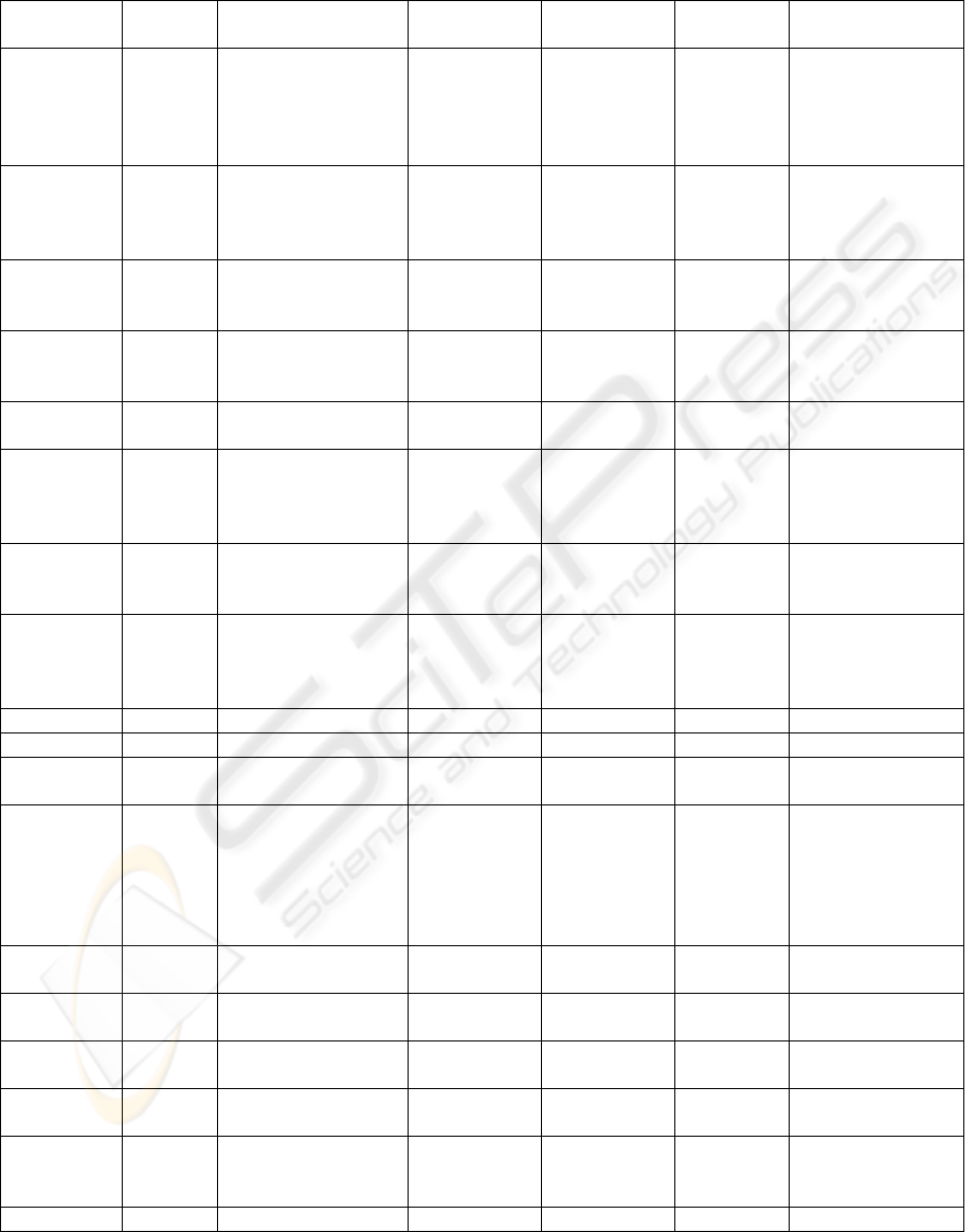
Table 1: Comparison of Profibus and WorldFIP with other important fieldbus protocols.
Fieldbus Topology Physical medium Data rate Distances Nodes per
segment
Network access
Profibus Bus Shielded Twisted Pair 9.6 Kbps
19.2 Kbps
93.75 Kbps
187.5 Kbps
500 Kbps
1200 m
1200 m
1200 m
600 m
200 m
32 - Token
- Master-slave
polling
WorldFIP Bus Shielded Twisted Pair
Optical fiber
31.25 Kbps
1 Mbps
2.5 Mbps
5 Mbps
1900 m
750 m
500 m
32 Centralized
(bus arbitrator)
AS-I Bus
Tree
Star
Two wires 167 Kbps 100 m 32 Master-slave polling
Bitbus Bus Twisted Pair
Optical fiber
62.5 Kbps
375 Kbps
1.5 Mbps
1200 m
300 m
29 Master-slave polling
CAN Bus Twisted Pair 50 Kbps up to
1 Mbps
1000 m up to
40 m
127
64
CSMA/CD with
arbitration
ControlNet Bus
Ring
Star
Coaxial
Optical fiber
5 Mbps
5 Mbps
1000 m
3000 m
48 CTDMA
(Concurrent Time
Domain Múltiple
Access)
DeviceNet Bus Twisted Pair 125 Kbps
250 Kbps
500 Kbps
500 m
250 m
100 m
64 CSMA/CD
Firewire
(IEEE 1394)
Bus
Tree
Six wires
Optical fiber
100 Mbps
200 Mbps
400 Mbps
800 Mbps
700 m 63 Time slots
HART Bus Two wires 1200 bps 3000 m 30 Master-slave polling
Interbus-S Ring Twisted Pair 500 Kbps 400 m 256 Token
J1939 Bus Shielded Twisted Pair 250 Kbps CSMA/CD with
arbitration
LonWorks Bus
Ring
Free
Twisted Pair
Optical fiber
Power line
Coaxial
Radio
Infrared
78 Kbps up to
1.25 Mbps
2700 m up to
130 m
64 CSMA/CA
M-Bus Bus Two wires 300 bps up to
9600 bps
1000 m 250 Centralized
Measurement
Bus
Bus Four wires 110 bps up to
1 Mbps
500 m 31 Master-slave polling
Modbus Bus Twisted Pair 300 bps up to
19.2 Kbps
1 Km 248 Master-slave polling
M3S Bus Six wires CSMA/CD with
arbitration
P-Net Ring Shielded Twisted Pair 76.8 Kbps 1200 m 125 - Token
- Master-slave
polling
Seriplex Bus Four shielded wires 98 Kbps 1500 m 300 Master-slave polling
ICINCO 2004 - SIGNAL PROCESSING, SYSTEMS MODELING AND CONTROL
48
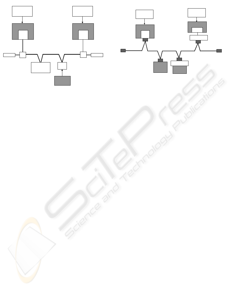
Emulator PLC
bus arbitrator
TSX
FPC 10
PC
Tap
box
Connection
cable
Terminator
Protocol
Analyzer
TSX
FPC 10
PC
Connection
cable
TBX
8Inputs/8Outputs
Test
point
Equipment
under test
Trunk cable
Terminator
Tap
box
Figure 1: Block diagram of the WorldFIP network used to
check the designed device.
3 DESIGN OF A FIELDBUS
INTERFACE USING FPGA
The implementation of fieldbus communication
processors using SRAM FPGAs has a lot of
advantages derived from its reconfiguration
capability. The most important are:
- The FPGA programming code can be easily
improved adding new functions.
- Little changes in bus definitions (frame
format, transmission headers, etc.) can be
easily solved changing the software
description of the interface, avoiding the
economic cost associated to the equipment
renewal.
- It is possible to design devices for different
fieldbuses with similar physical layers
making little changes in the programming .
Taking into account these advantages, the
development of reconfigurable fieldbus interfaces
results in a very interesting project. Thus, the
authors have worked in the implementation of the
basic communication functions for two very well
known protocols (Profibus and WorldFIP) using a
SRAM FPGA. A Profibus slave station and the basic
services (writing buffer, reading buffer and transfer
buffer) of a WorldFIP consumer/producer station
have been implemented over the same hardware
(FPGA). Thus, this compatible device is able to
transmit and receive any frame in right way over any
WorldFIP and Profibus network.
There are several factors to be considered in the
selection of the FPGA for this application. The most
important are the cost, the operation frequency and
the available logic resources. The fieldbuses operate
Master station
Profibus
boiard
PC
Terminal
connector
Protocol
Analyzer
(Bus spy)
Serial port
PC
FPGA
(Profibus
Slave station)
Profibus network
Level and impedance
matching circuit
Terminal
connector
PLC
(Master
station)
Test
point
Level and impedance
matching circuit
Figure 2: Block diagram of the Profibus network used to
check the designed device.
at low data rates (in this work 9.6 Kbps for Profibus
and 1 Mbps for WorldFIP) and then a high speed
FPGA is not required. By other side, fieldbus
protocols manage many variables that must be
stored. So, in order to simplify the design, it is
suitable the use of a FPGA with embedded memory
blocks. Taking into account these two aspects and
the cost, the FPGA FLEX 10K20RC240-4 from the
ALTERA manufacturer was chosen for
implementing the communication processor of this
project [ALTERA, 1998].
The design was developed using the
MAX+PLUS II CAD tools from ALTERA
[ALTERA, 1994] and the system was specified in
VHDL (Very high speed IC Hardware Description
Language) [IEEE, 1994] to allow the portability of
the design to other FPGA devices.
4 IMPLEMENTED DEVICE
To check the good working of the implemented
device, two networks was used with the structures
represented in Figures 1 and 2.
In the WorldFIP network there are two PCs
connected to the bus through a TSX FPC 10 board
from the Telemecanique manufacturer. One of this
PCs runs a software that emulates the behavior of a
PLC with the functionality of bus arbitrator. The
other one is a protocol analyzer used to capture all
the frames transmitted on the bus and so to verify
the good working of the implemented device
(connected to the test point). Also a TBX module
from Telemecanique with 8 inputs and 8 outputs is
used to generate traffic on the network and so to
study the working of this protocol.
IMPLEMENTATION OF A DEVICE COMPATIBLE WITH DIFFERENT FIELDBUSES USING RECONFIGURABLE
CIRCUITS
49
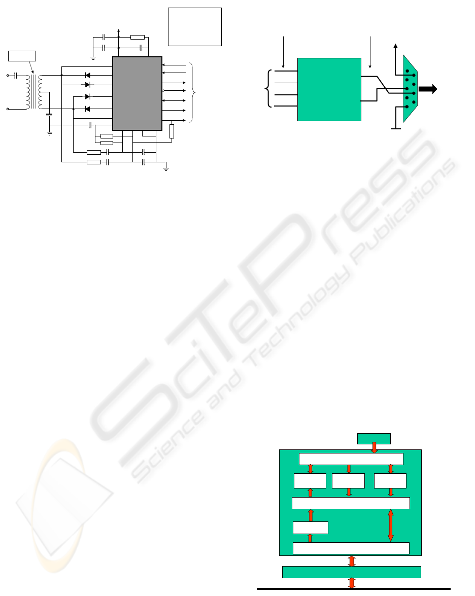
Vcc
TPC
A
AH
AL
BL
BH
C
RTS
TXD
CONSEM
/ERPHY
CK2FR
CDO
RXD
Gnd2Gnd1INAINB
CREOL
18
3
B
Bus WorldFIP
4
10 KΩ
10 KΩ
22.6 KΩ
22.6 KΩ
2
1
19
17
14
2.2 MΩ
5
16
615
FPGA
13
12
11
10
9
8
4.02 Ω
7 20
n1
n2
n3
n1 = n2
n3 = 1.5 (n1 + n2)
150 nF
47 nF
LL 4448
LL 4448
47 nF
100 pF
100 pF
3.3 pF
3.3 pF
220 µF
47 µF
47 nF
Vcc (5 V)
RTS: Request To Send
TXD: Transmit Data
CONSEM: Transmiter Consumption
/ERPHY: Physical Error
CK2FR: Clock 2 FR
CDO: Carrier Detect Output
RXD: Received Data
TPC: Transmitted Power Control
Figure 3: Level and impedance matching circuit for the
WorldFIP fieldbus.
The Profibus network is made up of two PCs,
one PLC and the test point where the implemented
device based on the FPGA is connected for its
verification. One PC has a Profibus board from
Siemens that is programmed for polling the data
produced for the sensor connected to the designed
communication interface (FPGA). The other PC runs
an application, designed by the authors, that allows
the capture (using the serial port with a data rate
limited to 9.6 Kbps) and analysis of all the frames
circulating on the bus (protocol analyzer). The PLC
is used as a master station that generates traffic in
the network and allows the study of the working of
this protocol.
4.1 Level and Impedance Matching
Circuits
Due to the electrical characteristics of Profibus,
WorldFIP and FPGA are not the same, it is
necessary to design different level and impedance
matching circuits (Figure 3 and 4) that convert the
signals present in the bus to TTL/CMOS signals
suitable for the FPGA and vice versa. This is the
unique change in the hardware required for
connecting the designed compatible device based on
FPGA to these two fieldbuses.
The WorldFIP matching circuit is based on an
integrated circuit from Telemecanique known as
CREOL and a transformer connected to the bus line.
In the case of Profibus networks a MAX485CPA
integrated circuit is used to make the conversion of
TTL/CMOS signals to Profibus signals (RS-485).
MAX485CPA
RO
/RE
DE
DI
B
A
VCC
GND
1
2
3
4
8
5
VCC
GND
7
6
6
3
8
5
PROFIBUS
FPGA
Connector
DB9 female
Profibus
signals
TTL/CMOS
signals
Figure 4: Level and impedance matching circuit for the
Profibus fieldbus.
4.2 The Fieldbus Communication
Processor
To get a compatible device between WorldFIP and
Profibus networks two designs were specified using
VHDL. The block diagrams of these two designs are
shown in Figures 5 and 6.
The WorldFIP design consists of a
transmitter/receiver circuit, a receiving buffer, a
WorldFIP control system, the consumed and
produced data bases, an identifier index and a
variable access protocol. The transmitter sends data
adding the Frame Starting Sequence (FES) and the
Frame End Sequence (FES) established in the
WorldFIP protocol. The receiver detects the frames
circulating by the bus and delivers them to the
receiving buffer checking the corresponding Frame
Check Sequence (FCS).
RECEIVING
BUFFER
TRANSMITTER/RECEIVER CIRCUIT
CONSUMED
DATABASE
USER
FPGA
LEVEL AND IMPEDANCE MATCHING CIRCUIT
BUS
WorldFIP CONTROL SYSTEM
IDENTIFIER
INDEX
PRODUCED
DATABASE
VARIABLE ACCESS PROTOCOL
Figure 5: Scheme of the implemented WorldFIP interface.
ICINCO 2004 - SIGNAL PROCESSING, SYSTEMS MODELING AND CONTROL
50
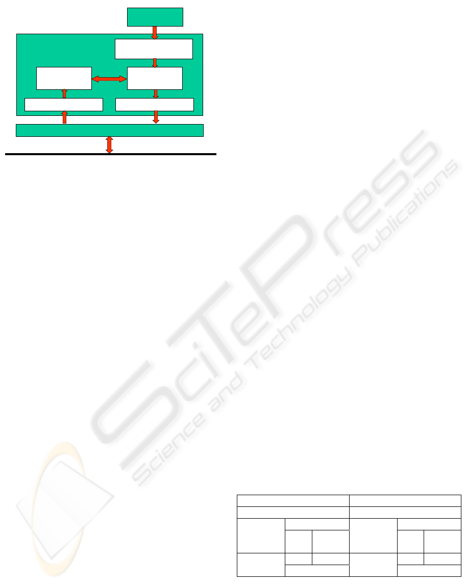
RECEIVER CIRCUIT TRANSMITTER CIRCUIT
RECEPTION
APPLICATION
TRANSMISSION
APPLICATION
SENSOR BUFFER
SENSOR
FPGA
LEVEL AND IMPEDANCE MATCHING CIRCUIT
BUS
Figure 6: Scheme of the implemented Profibus interface.
The receiving buffer is used to temporarily store
the last frame received that will be processed by the
WorldFIP control system. To implement this circuit
a cycle shared double port RAM is used to allow a
simultaneous access to this buffer. The WorldFIP
control system processes the frames stored in the
receiving buffer and runs the required actions
according to the protocol. The values of the
consumed and produced variables (set in the
configuration of the device) are stored in the
consumed and produced databases that are also
implemented with a cycle shared double port RAM.
The identifier index contains all information about
the identifiers of the consumed and produced
variables (identifier number, type, length of the
variable and its address in the corresponding
database). Finally, there is an interface between the
external circuits (the corresponding sensors and
actuators) and the designed communication
processor that is implemented in the variable access
protocol block.
A WorldFIP network with a data rate of 1 Mbps
was used for this work. The bus uses Manchester
coding (each half symbol has different logic level).
Thus, the system requires two clocks, the main one
of 10 MHz used by the receiver (take 5 samples per
half symbol) and another of 2 MHz used to control
the data sending.
The Profibus design comprises a receiver circuit,
a transmitter circuit, a reception application module,
a transmission application module and a sensor
buffer. The receiver circuit manages the reception of
the characters conforming the frames transmitted by
the bus. When a byte is received, this circuit
indicates to the reception application module if it is
valid or not. The reception application module takes
the valid data bytes and analyzes them to verify the
destination address and the type of frame. It checks
for possible errors in transmission (uses a check
field of the frame) and if there are not errors the
transmission application receives the information of
the received frame. Then, the transmission
application module generates the corresponding
response frame that is sent to the transmitter circuit
so that it conforms and transmits the frame
characters. This design includes a sensor buffer to
store the last measurement from a specific sensor.
This value is read by the transmission application
module to generate the adequate response frame
when a request frame asking for this data is received
in the device.
The data rate of the Profibus network used in this
work is 9.6 Kbps (limited by the protocol analyzer
station that uses the serial port to capture the frames
circulating by the bus). Then, the clock signal
frequency used by the receiver and transmitter
circuits is 9.6 KHz too. It is resynchronized with the
bus every time a new character is detected.
4.3 Technical Comparison
Table 2 shows a comparative of the FPGA logic
resources required to implement the WorldFIP and
the Profibus communication processors.
It can be observed that the average of the logic
used resources is very similar in both cases. The
WorldFIP interface uses more memory blocks and
interconnection resources because it needs to store
more variables (several consumed and produced
data, identifier index, variables of management to
indicate the presence of a station in the bus, etc.)
than in the case of Profibus (only the data stored in
the sensor buffer).
The occupation of resources in the FPGA used in
this project is very high. Thus, it is adequated for the
implementation of simple communication interfaces
(a Profibus slave station and a WorldFIP
consumer/producer station with the basic services
and producing only one variable). When more
functions must be implemented (for example, the
design of a Profibus master station, a WorldFIP
Table 2: FPGA resources used in this project.
WORLDFIP PROFIBUS
Resources of FPGA Resources of FPGA
Logic Logic Interconn.
Logic
Cells
Memory
Blocks
Interconn.
Logic
Cells
Memory
Blocks
94% 60% 94% 33% 74%
82%
56%
81%
consumer/producer station with all the services
provided by the data link layer or a WorldFIP bus
arbitrator station), it is required the use of a bigger
FPGA with more logic resources.
IMPLEMENTATION OF A DEVICE COMPATIBLE WITH DIFFERENT FIELDBUSES USING RECONFIGURABLE
CIRCUITS
51
4.4 Simulation
To verify the behavior of the designed
communication interface, many functional/timing
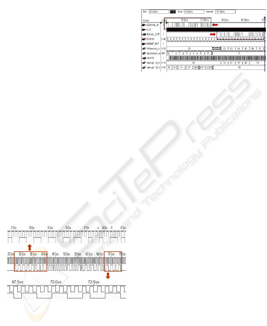
simulations and tests were developed. Figure 7
shows an example of the simulation results of the
transmitter circuit of the WorldFIP communication
processor where the generation of the FSS (Frame
Starting Sequence) and the FES (Frame End
Sequence) can be observed. Figure 8 shows other
example of simulation for the Profibus interface
where a received request frame and the
corresponding response frame generated by the
Profibus communication interface can be observed.
5 CONCLUSIONS
In this paper the authors propose a solution to design
compatible devices for different fieldbuses using
reconfigurable circuits. In this work it is
demonstrated that it is possible to get a device that
can be connected to two of the most important
fieldbuses used in Europe in industrial control
processes like WorldFIP (French standard) and
Profibus (German standard). This device is designed
using a FPGA (Field Programmable Gate Array)
from ALTERA. It is programmed with the necessary
code (in VHDL) to specify the services of a Profibus
slave station and the basic services (writing buffer,
reading buffer and transfer buffer) of a WorldFIP
consumer/producer station.
Figure 7: Simulation results of the WorldFIP transmitter
circuit.
REQUEST FRAME
RESPONSE FRAME
Figure 8: Simulation results for the Profibus interface.
Thus, this device can be used either in a
WorldFIP network or in a Profifus network without
changes in the hardware (it is only necessary to
change the connector that contains the adequate
level and impedance matching circuit). It supposes a
great money saving when a user needs to change the
protocol of its fieldbus system and also an
improvement in the interconnection between the
fieldbus devices that can be supplied in the market.
The FPGA used in this work is a low cost circuit
with limited logic resources. The use of the
resources is very high as it is shown in section 4.3.
Thus, to implement more complex devices like
Profibus master stations, WorldFIP bus arbitrator
stations or WorldFIP consumer/producer stations
with the complete seven services that can be
provided in the protocol, it is necessary to use a
FPGA of higher level with more logic resources and
interconnection elements and also more expensive.
In this line of research, it would be very
interesting for future works to get the
implementation of multiple fieldbus protocols in a
unique FPGA. Also it would be possible to
implement an intelligent reception module able to
identify the type of network from the analysis of the
received frames to automatically use the adequate
protocol. Thus, a total compatibility of the field
devices would be achieved with the advantages that
it supposes. A problem for getting this aim would be
that the used FPGA should have a lot of logic
resources and interconnection elements and its price
would be very high. But it can be solved with a
design of a more complex device with multiple
FPGAs and may be other reconfigurable devices.
REFERENCES
AFNOR, 1990. Standard NFC 46-601 to 605: Bus FIP
pour échange d’information entre transmetteur,
actionneur et automate.
FSS
FES
ICINCO 2004 - SIGNAL PROCESSING, SYSTEMS MODELING AND CONTROL
52

CENELEC, 1996 (December). Standard EN 50170:
General purpose field communication system.
Domínguez, M.A., 2000. Contribution to the analysis of
the data link level in communication protocols for
standard fieldbuses (In Spanish), Ph.D. Thesis,
Department of Electronic Technology, University of
Vigo, Spain.
IEC, 1993. Standard IEC 1158: Fieldbus standard for use
in industrial control system.
IEEE, 1994 (June). IEEE 1076-1993: IEEE Standard
VHDL Language Reference Manual, SH16840.
Lías, G., Valdés, M.D., Domínguez, M.A. and Moure,
M.J., 2000. Implementing a fieldbus interface using a
FPGA. In FPL’2000 10th International Conference on
Field Programmable Logic and Applications. Villach,
Austria, August 2000, Lecture Notes in Computer
Science 1896, R.W. Hartenstein, and H. Grünbacher
(Eds.), ISBN 3-540-67899-9, Springer-Verlag, pp.
175-180.
PROFIBUS Nutzeorganisation, 1991 (April). Profibus
standard: Translation of the German standard DIN
19245 (part 1 and part 2), PROFIBUS
Nutzeorganisation e.V. Wesseling Germany.
ALTERA, 1998. ALTERA Data Book, Altera Corporation,
San José (CA).
ALTERA, 1994 (July). MAX+PlusII Getting Started,
Altera Corporation.
IMPLEMENTATION OF A DEVICE COMPATIBLE WITH DIFFERENT FIELDBUSES USING RECONFIGURABLE
CIRCUITS
53
