
A FPGA Learning System combining
Hardware and Software Tools
M. Dolores Valdés
1,2
, M. José Moure
1,2
, Camilo Quintáns
1,2
,
Bruno Pérez
2
and Enrique Mandado
1,2
1 University of Vigo. Dpt. of Electronic Technology. Spain
2 University of Vigo. Institute for Applied Electronics. Spain
Abstract. FPGA including very complex digital blocks are possible nowadays
due to digital integrated circuits progress. FPGA fundamentals and character-
istics are not easy to explain because they have a lot of interrelated concepts.
By this reason FPGA learning is usually based on a family of a particular
manufacturer and doesn’t give a general view of configurable devices. Due to
that it is essential for the electronic learning community to dispose of tools fa-
cilitating the learning process of the fundamentals of the FPGA’s and the de-
sign of systems based on them. The learning system we describe in this paper
combines a tutorial with a hardware and software tools to achieve a friendly
interface with a PC to facilitate FPGA distance learning for students with a
basic knowledge of digital electronics and VHDL.
1 Introduction
FPGA (Field Programmable Gate Array) are very large scale integration digital
circuits (VLSI) and due to that they constitute a complex technology including many
interrelated concepts. By this reason FPGA education is normally based on particular
devices from just one manufacturer. But although this approach gives to the student
a practical education, it does not give the global vision which is necessary to be able
to specify and design FPGA based systems.
At the same time, laboratory experiences use developing software owner tools and
actual FPGA development systems do not have a communication channel to transfer
information between the FPGA and the computer. Due to that external electronic
instruments are needed to check the application.
This paper presents an FPGA learning system combining a tutorial with hardware
and software tools providing a friendly interface with a personal computer. The sys-
tem constitutes a useful distance learning tool.
Dolores Valdés M., José Moure M., Quintáns C., Pérez B. and Mandado E. (2004).
A FPGA Learning System combining Hardware and Software Tools.
In Proceedings of the First International Workshop on e-Learning and Virtual and Remote Laboratories, pages 79-88
DOI: 10.5220/0001150200790088
Copyright
c
SciTePress
2 General Description
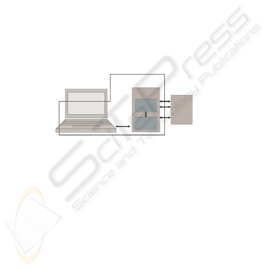
Fig. 1 shows the block diagram of the system, including a hypermedia tutorial and
hardware and software tools related by means of a set of practical examples.
The hardware tools are:
• A mainboard with a FPGA and a USB2.0 driver [7].
• An expansion card including specific peripheral devices (analog to digital
and digital to analogue converters, LCD display, keyboard, etc.).
The software tools are:
• The mainboard control software for the FPGA configuration and the
communication channel implementation.
• The Altera’s Quartus II Web Edition tool for describing and synthesizing
circuits using an schematic capture tool and a VHDL language compiler.
Fig. 1. Block diagram of the FPGA learning system
The tutorial is a hypermedia application running on a personal computer. It drives
the student from the different FPGA basic concepts to actual FPGA digital system
design. The set of practical examples included in the hypermedia tutorial are ori-
ented to APEX family circuits and tools from Altera but their functionality is gener-
ally enough to be used with de devices of different manufacturers.
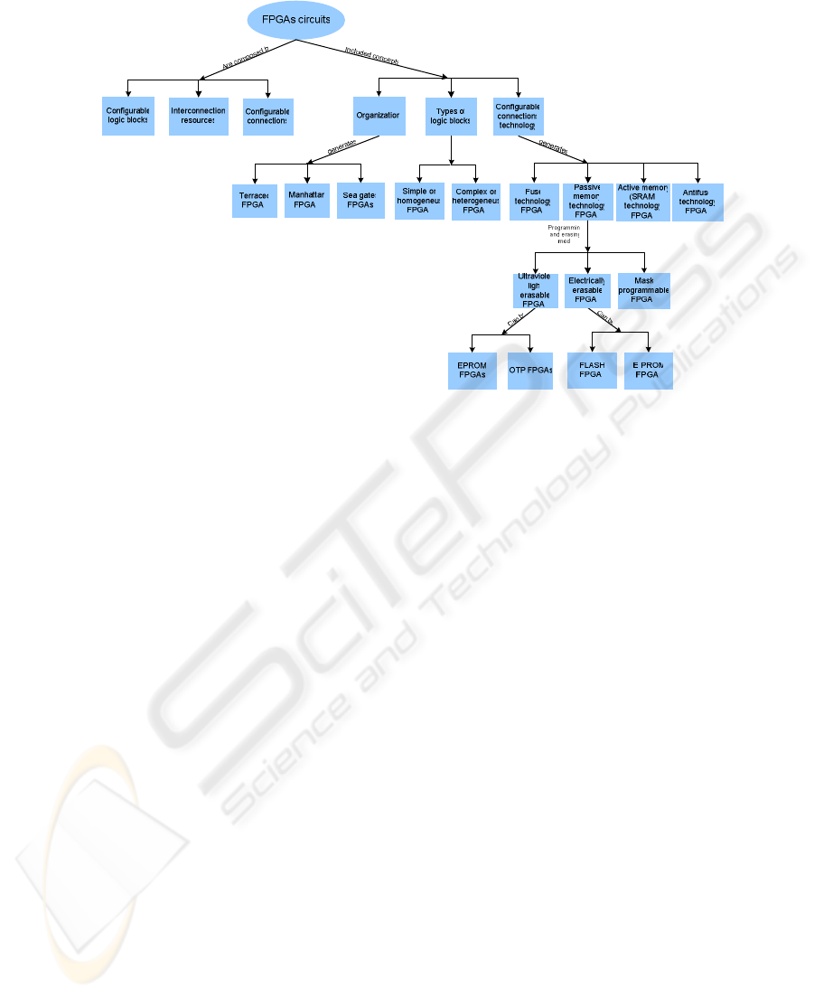
3 Hypermedia Tutorial
Due to the fact that FPGA constitute a complex technology [2], the hypermedia sys-
tem has been done using the method developed by the Institute for Applied Electron-
ics of the University of Vigo [9] to obtain the descriptive model of a complex tech-
nology. This method comprises four main stages:
• Firstly, many different representative systems or devices are chosen.
USB2.0
USB2.0
USB2
USB2
-
-
FPGA
FPGA
Development system
Development system
Development
board
USB
Controller
FPGA
Expansion
Cards
.
.
.
.
.
.
Tutorial
Tutorial
Control Panel
Control Panel
DesignvSoftware
DesignvSoftware
USB2.0
USB2.0
USB2
USB2
-
-
FPGA
FPGA
Development system
Development system
Development
board
USB
Controller
FPGA
Expansion
Cards
.
.
.
.
.
.
.
.
.
.
.
.
.
.
.
.
.
.
Tutorial
Tutorial
Control Panel
Control Panel
DesignvSoftware
DesignvSoftware
78
generates
Fig. 2. FPGA circuit conceptual map
• In the second stage the selected systems are analyzed in detail to define the
concepts associated to the technology. This task is carried out in two differ-
ent phases:
- All the common characteristics are determined and classified to define
the general characteristics or basic concepts of the complex technology.
- In the second phase the basic concepts are characterized (including
functionality, implementation, architecture, etc.) taking into account
the specific characteristics of each particular system in such a way that
the subconcepts of the descriptive model are obtained as well as its de-
pendence relations. The same subconcept can be present in different
systems but the set of subconcepts associated to each system can be dif-
ferent.
• In the third stage all the basic concepts and subconcepts are structured to
obtain the descriptive model.
• Finally, the descriptive model must be tested to verify its ability to describe
not only the systems chosen to obtain the model but, all the commercial sys-
tems known.
Once the descriptive model is obtained, it is necessary to use a graphical represen-
tation of it. So we studied the application of conceptual maps being used at present
only to describe general human knowledge areas [3] [4] [5] [6].
79

Fig. 2 shows the FPGA’s conceptual map. The concepts are interrelated and due
to that it is interesting to describe the map with hypermedia using the map concepts
as key words to achieve a non sequential access to the information. Every concept is
explained using web pages combined with a browser to implement the hypermedia
system. Every concept is described using text, pictures, diagrams and videos. The
user can navigate through the lessons using a friendly interface [1]. To simplify
navigation, every lesson has linkages with a glossary, including a multimedia defini-
tion of the different concepts.
4 USB2 – FPGA Development System
4.1 Hardware Description
Actual FPGA development systems do not have a high speed communication chan-
nel for information transfer between the FPGA device and the computer development
tool. To overcome this limitation, the authors of this paper developed the USB2-
FPGA board with the following features:
• A communication channel based on the USB2 serial bus. This channel
can be used for the configuration of the FPGA as well as to support a
high speed general purpose communication channel between the USB2-
FPGA board and the PC.
The main advantages of the USB2 bus are:
- It reduces the configuration time.
- It provides a high speed channel support to communicate the con-
figurable device with the PC.
- It requires the development of a control system in the FPGA to
achieve the control of the bidirectional data transfer but such a sys-
tem is very simple and consumes just a few logic resources.
- It is a standard connection available in a wide range of commercial
equipments.
• The input/output pins of the FPGA are accessible. In order to facilitate
the connection of peripherals required in different applications all the
input/output pins of the FPGA can be accessed through standard con-
nectors.
Fig. 3 and Fig. 4 show a photo and a schematic of the developed board. The
main parts are:
• The FPGA APEX EP20K100EQC240-2X from Altera.
• The USB2.0 controller from Cypress.
• The E
2
PROM EPC2LC20 from Altera to storage the configuration file.
80
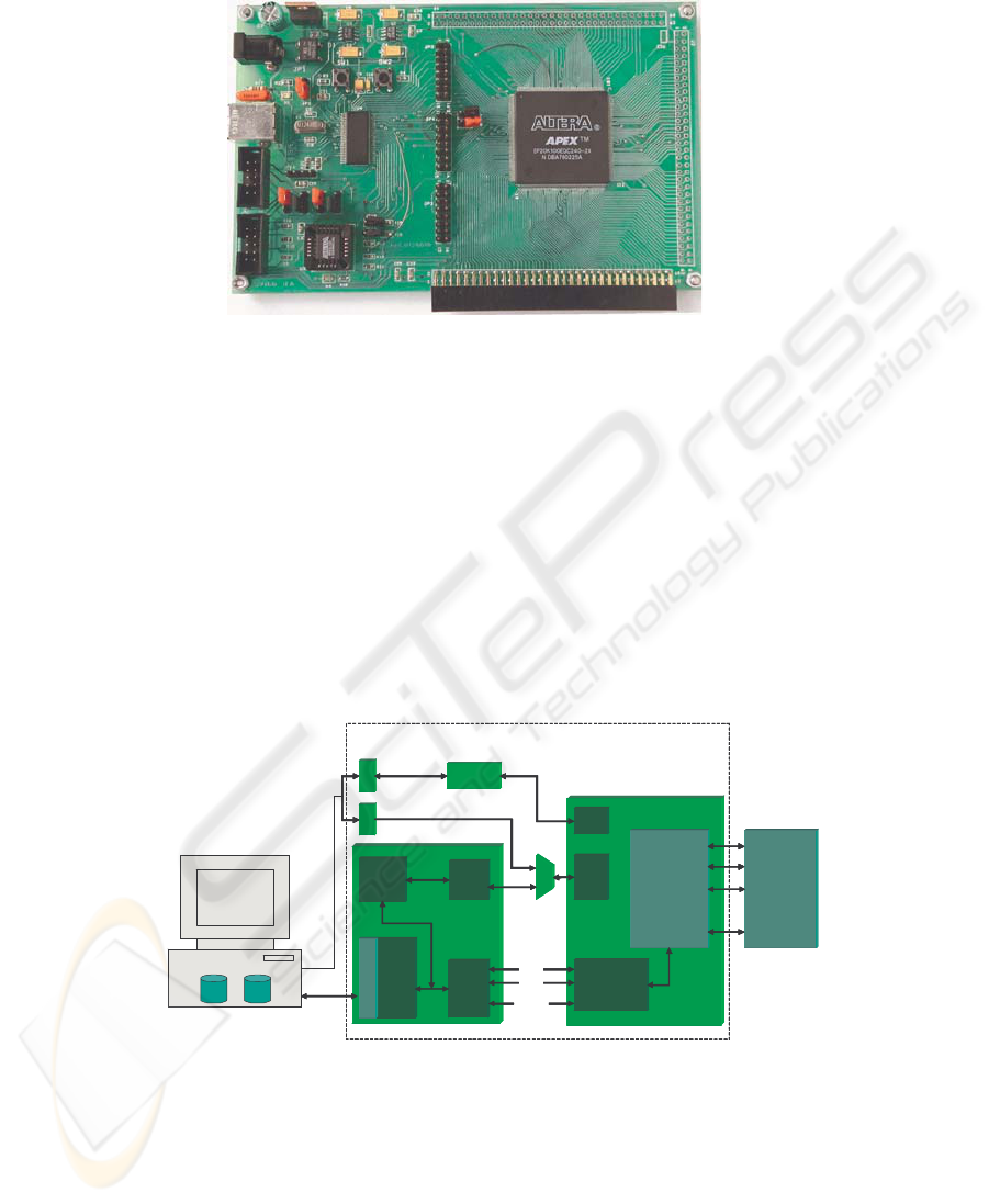
Fig. 3. Photography of the USB2-FPGA development board
• A +5V DC voltage source coming from an external AC/DC adaptor or
from the USB connection. 1,8V and 3,3V DC voltages can be obtained
from the +5V DC voltage source.
• Configuration mode selector. The board supports three configuration
modes: from the PC through the USB channel, from the PC through the
JTAG interface (passive serial mode) and from an E
2
PROM memory.
• USB connector.
• JTAG connector.
• Three 64 pins connectors to access all the input/output pins of the FPGA.
Different expansion cards containing specific peripheral devices can be
connected to the FPGA through the connectors.
Fig. 4. Schematic of the USB2-FPGA development board
USB
Controller
USB
SIE
U
S
B
Port B
Port D
Port C
µC
Parallel Bus
Control
Port A
FPGA
Communication
Controller (IP)
User
Application
.rbf.exe
User
Expansion
Cards
.
.
.
USB2-FPGA Development Kit
Data
PS
E
2
PROM
JTAG
PP
USB
Controller
USB
SIE
U
S
B
Port B
Port D
Port C
µC
Parallel Bus
Control
Port A
FPGA
Communication
Controller (IP)
User
Application
.rbf.exe
User
Expansion
Cards
.
.
.
.
.
.
USB2-FPGA Development Kit
Data
PS
E
2
PROM
JTAG
PP
81
4.2 Software Description
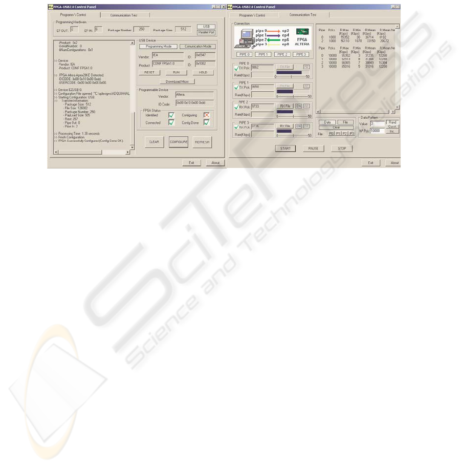
A program named “USB2-FPGA Control Panel” has been developed to support the
USB2-FPGA board configuration and communication. Fig. 5 shows its graphic user
interface. As can be observed the main functions of the program are the FPGA con-
figuration or programming (Fig. 5a) and the supervising of the data transfer between
the FPGA and the PC (Fig. 5b).
Fig. 5. USB2-FPGA Control Panel. (a) Programing mode (b) Communication mode
FPGA configuration timing is an important parameter for applications where the
FPGA must be reconfigured many times. The programmer included in the “USB2-
FPGA Control Panel” shows a significant reduction of the programming timing. In
order to verify its performance a comparison with the Altera Quartus II programmer
was made. The test conditions and the results that demonstrate the superiority of the
developed programmer are shown in Table 1.
In the communication mode (Fig. 5b) the USB2-FPGA Control Panel verifies
the data transfer between the computer and the FPGA and supervises the transfer
rate and the state of the FIFO memories (inside the USB controller) that temporally
store the received and sent data.
To use the USB2-FPGA development system the channel communication be-
tween the computer and the FPGA must be establish and the FPGA must be pro-
grammed. This process includes the following stages:
• The PC initializes the USB controller through the USB2.0 channel.
• The PC configures the SIE unit of the USB controller and its internal mi-
crocontroller takes the control . The SIE unit includes the FIFO memories
supporting the temporal storage of the transferred data.
• The internal microcontroller of the USB controller programs the FPGA
transferring the configuration file from the PC to the device through the
SIE unit and the JTAG interface .
(a)
(b)
82
• The USB controller gives the control of the SIE unit to the FPGA and the
communication between the user application and the PC is established.
Table 1. Comparison of the programmers performance
Test conditions Results
Quartus II:
· ByteBlasterMV (LPT1):
· File format: *.sof
· Size: 121 KB
· Timing-> 4.1 seg.
Operating system: Windows XP
PC:
Processor: Pentium® IV 2.40 GHz.
Frequency: 2.42 GHz
RAM: 256 MB DDR
Configuration file:
File format: .rbf
Size : 123 KB
Device:
APEX20K100EQC240-2X
Programs:
· Quartus II Versión 1.1.
· FPGA-USB2.0 Control Panel v1.1
USB2.0-FPGA Control Panel:
· File format : *.rbf
· Size: 123 KB
· Timing-> 1.31 seg. (USB2.0)
5 FPGA Applications Self-learning Laboratory
The USB2-FPGA development system can be considered as a laboratory intended for
FPGA applications self-learning by means of the resolution of practical exercises of
increasing complexity. It is supposed that the user knows the basic digital blocks
(logic gates, flip-flops, multiplexers, decoders, counters, memories, etc.) as well as
the basis of the VHDL hardware description language.
In this way the development system has the following objectives:
• Make easy the learning of FPGA based systems design methods.
• Apply the design methods using the Quartus II Web Edition design tools
from Altera.
• Improve the VHDL design skills.
A set of developed practical exercises is showing next. Simple digital systems of
the first exercises are part of the more complex systems of the latest exercises.
Exercise 1: Digital control system of a 4x4 keyboard.
Exercise 2: Digital interface of a PS2 keyboard.
Exercise 3: Digital control system of a LCD display.
Exercise 4: LIFO and FIFO memories.
Exercise 5: Basic calculator using the systems of exercise 2 and 3.
Exercise 6: Manchester serial transceiver with CRC.
Exercise 7: Control system of a PWM analog to digital converter.
Exercise 8: Digital control system of a successive approximation analog to
digital converter.
Exercise 9: Home alarm emulator using the systems of exercises 2, 3, 6, 7
and 8.
Exercise 10: FIR filter using the systems of exercises 7 and 8.
83

The design process of FPGA based systems includes the main stages referred
next. In the USB2-FPGA development system most of the design stages use the
Quartus II Web Edition design tools from Altera.
• Description
The system behavior and/or structure is defined from the design specifica-
tions. Schematics are used to describe the system structure and hardware de-
scription languages, like VHDL or Verilog, are used for the behavioral descrip-
tion. Usually a joint description combining both structural and behavioral ones is
used to define a specific system.
• Compilation
During compilation a netlist containing all the system components and their
interconnections is obtained, the right connection of the components is verified
and possible syntax errors are detected. Optionally, the netlist can be optimized
in order to improve the logic and interconnection resources usage.
The resultant netlist is used for the implementation and verification stages.
• Implementation
In this stage FPGA logic resources are assigned to the different elements of
the netlist (mapping process), placed and interconnected (place & route process
or fitting process). Besides, the FPGA programming file is generated and a new
netlist containing the delay of all signals is obtained.
Using the updated netlist a timing simulation or a timing analysis can be ac-
complish in order to verify the right operation of the designed system. If verifi-
cation results are the expected ones the FPGA can be programmed and the de-
sign is finished.
• Verification
Verification stage can be divided into three different processes: functional
simulation, timing simulation and timing analysis. By means of functional simu-
lation the system behavior can be verified without any timing consideration.
When good results are reached the system can be implemented and if not the
description must be modified.
Timing simulation and analysis take place after the implementation. Accord-
ing to the results of these processes the following actions must be accomplished
by the designer:
-
When the system does not match the design specifications the descrip-
tion must be modified in order to correct possible errors.
-
If the system does not work properly due, for example, to excessive
signal delays, one of these solutions must be executed:
-
Back to the compilation or implementation stages to change options.
-
Back to the description stage if the results are not the expected once
the compilation and implementation options have been modified.
• Programming
The FPGA is programmed using the USB2-FPGA Control Panel tool.
84
5.1 Virtual Logic Analyzer
Besides the hardware and software resources described above, a virtual logic ana-
lyzer intended to verify the designed system behavior have been developed [8].
The logic analyzer combines a hardware support and a software human machine
interface (HMI) that runs in the PC.
The hardware support is implemented in the FPGA. It is made up of the analyzer
input pins (data acquisition channels), a data acquisition memory and the communi-
cation processor that take charge of the acquired data transfer from the FPGA to the
PC through the USB2.0 connection. This hardware is a module of a design library
and must be included in the system that is being designed during the description
stage. It consumes few logic and interconnection resources and does not inhibit the
implementation of the proposed practical exercises.
To use the logic analyzer the acquisition channels (input pins of the logic ana-
lyzer) must be connected to the desired nodes of the implemented system. The nodes
can be external (FPGA output pins) or internal signals. In the first case the output
signals of the designed system must be wired to the input channels of the analyzer,
just like an external instrument. In the case of internal node verification connections
must be defined during the description stage. This type of verification can not be
achieved with an external measurement system.
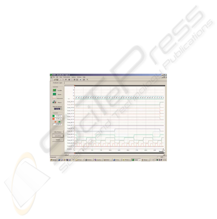
Fig. 6. Logic analyzer human machine interface
Fig. 6 shows the logic analyzer human machine interface (HMI). It is a Visual
C++ application for Windows, combining a graphic editor, where acquired signals
are represented, with a control panel to configure the logic analyzer operation
modes.
85

6 Conclusions
The main characteristics of the system are:
• It provides an efficient learning method combining a multimedia tutorial
system with a hardware to achieve not only a theoretical education but a
practical training with a good cost/performance relation.
• It is appropriate to achieve asynchronous distance learning due to the low
cost of the development board components and the free available software.
• The system configurability including a high number of input/output pins.
• The diversity of internal and external resources providing a high flexibility.
• The USB2.0 interface providing a very fast communication channel between
the board and the PC.
• The virtual logic analyzer to test internal and external nodes of the designed
system.
References
1. Alessi S.M., Trollip S.R.: Multimedia for learning. Alling and Bacon, Massachusetts, 3a
ed., (2000)
2. Brockman J.M., "Complex Systems and Emergent Technologies", Report of the Center for
Integrated Design Seminar, June 29, 1998
3. Novak Joseph D.: Concept maps and Vee diagrams: two meta-cognitivies tools for science
and, mathematics education. Instructional Science, 19, 29-52. (1990)
4. Novak Joseph D.: Clarify with concept maps. The Science Teacher, 58(7), 45-49, (1991)
5. Novak Joseph D., Gowin D.B.: Learning to learn. Cambridge University Press,
Massachusetts, USA, (1988)
6. Ontoria A. et al.: Mapas conceptuales. Una técnica para aprender. Narcea S.A Madrid
(2000)
7. Quintáns C., Valdés M.D., Moure M.J., Mandado E.: Sistema de desarrollo de aplicaciones
electrónicas basado en dispositivos lógicos configurables y en el bus serie universal. Paten-
te P200301238. Mayo 2003
8. Quintáns C., Moure M.J., García-Valladares R., Valdés M.D., Mandado E.: A Virtual
Instrumentation Lab Based on a Reconfigurable Coprocessor. IMTC 2004 – Instrumenta-
tion and Measurement Technology Conference. Italy, Mayo 2004
9. Valdés M.D., Moure M.J., Mandado E.: Hypermedia: a tool for teaching Complex Tech-
nologies. IEEE Transactions on Education. No 4. Noviembre 1999
86
