
APPLICATION OF DYNAMICALLY RECONFIGURABLE
PROCESSORS IN DIGITAL SIGNAL PROCESSING
Hrvoje Mlinaric
Faculty of electrical engineering and computing, Universiti of Zagreb, Unska 3, Zagreb,Croatia
Mario Kovac, Josip Knezovic
Faculty of electrical eneginering and computing, Universiti of Zagreb, Unska 3, Zagreb,Croatia
Keywords: Dynamically reconfigurable processor, YUV-RGB conversion, processor architectures.
Abstract: The paper describes a new approach to processor construction, which combines a general purpose processor
and a program reconfigurable device, as well as its implementation in digital signal processing applications.
Significant flexibility and adaptability of such a processor is obtained through the possibility of varying the
components of the processor architecture. A simple change of architecture enables easy adaptation to
various applications in which such processors are used. Furthermore, to achieve even greater functionality, a
dynamic adjustment of the processor is enabled, by enabling the change of function of individual processor
components without the need to turn the processor off. The functionality change itself is conducted in such a
way that it is made in a single clock, which allows for a great flexibility of the processor, increases the
functionality and enables simple implementation in various applications. Such processor architecture is
broadly used in embedded computer systems for various multimedia, encryption and digital signal
applications.
1 INTRODUCTION
If we look at the modern computer systems from the
perspective of the processor embedded in such
systems, we can roughly divide them into two basic
groups: personal computers and server workstations,
and embedded computers. The basic difference
between these two computer systems is their
processing power. PCs and server workstations are
limited by the current technology, while the energy
consumption or their price is not important. Contrary
to that, for embedded computer systems the energy
consumption and even the price of the computer
systems are very important. Consequently, the
processors used in personal computers are unsuitable
for the construction of the majority of embedded
systems. In order to reduce the price and energy
consumption, embedded computers have simpler
processors whose power is significantly reduced,
which then reduces their price and energy
consumption. Such processors mostly satisfy the
requirements of embedded systems. If the need
arises for solving more complex problems,
specialised devices are added which can improve the
performance of the whole system, such as audio or
video signal decoding devices and others. The
downside of such additional devices is the increase
in price and energy consumption of the whole
system. Furthermore, the role of specialised devices
is narrowly specialised, which renders them unused
most of the time. The concept of this paper is to add
a specialised device to the processors, which will be
dynamically variable and functionally adaptable,
thus enabling the implementation of such a device in
a large number of applications, which will ultimately
lead to a reduction in price and energy consumption
of the whole system.
2 ARHITECTURE
The processor architecture consists of a 32 bit RISC
general purpose processor closely connected to a
dynamically reconfigurable device. The overall
architecture was tested and conducted on XILINX
Spartan-3 FPGAs (Field-Programmable Gate Array).
343
Mlinaric H., Kovac M. and Knezovic J. (2006).
APPLICATION OF DYNAMICALLY RECONFIGURABLE PROCESSORS IN DIGITAL SIGNAL PROCESSING.
In Proceedings of the International Conference on Signal Processing and Multimedia Applications, pages 343-346
DOI: 10.5220/0001570703430346
Copyright
c
SciTePress
The dynamically reconfigurable processor had to be
adapted to the Spartan-3 architecture limitations.
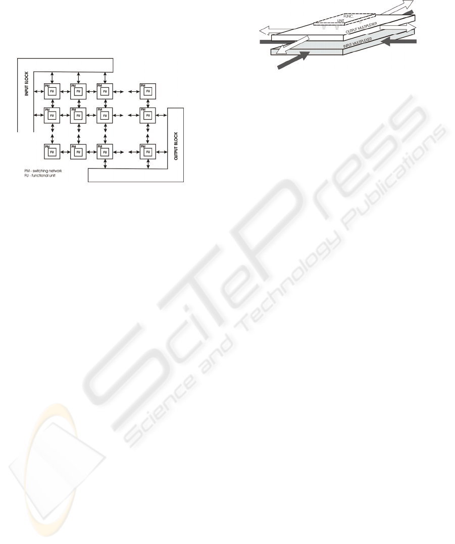
Figure 1 shows a block diagram of the dynamically
reconfigurable device described in this paper. There
are four major units which are characteristics of a
dynamically reconfigurable processor: input block,
output block, switching network and functional unit
Figure 1: Block diagram of the dynamically
reconfigurable device.
Due to the complexity of the entry-exit problem
and different functionalities, the input and output
blocks are separated. The purpose of the input and
output blocks are data retrieval, which are then
processed and the results stored. The switching
network connects all the system components and its
task is to provide the correct data flow through the
whole system. Each block of the switching network
is allocated to an appropriate functional block, with
the purpose to perform various mathematical
operations by which the appropriate functionality of
the whole device is achieved. There are two basic
types of functional blocks: multiplier and adder.
Apart from the four basic components, the system
requires three memory blocks: memory block for
input data storage, memory block for result storage
and memory block for registration of the variable
device configuration. The input and output memory
are separated in order to improve the system
performance. Having only one memory would slow
down the writing and reading of data, as it would
require that data be both written into and read from
the same memory within a single cycle.
The switching network controls the data flow
within the dynamically reconfigurable structure. The
alterable architecture of a switching network enables
data distribution across the entire device. Figure 2 is
a block diagram of a switching network. Each block
of the switching network is attached a functional
unit which is not a component of the switching
network. The switching network block input consists
of four inputs representing the links with four
adjoining elements surrounding the switching block.
Each of the four inputs can be connected to one of
the inputs in the functional unit through entry
multiplexers.
Figure 2: Block diagram of the switching network.
The central processing unit of a reconfigurable
device consists of a functional unit with the task to
process the data posted on its entries. During each
clock the functional units process two new pieces of
entry data and generate a result. The functional unit
consists of two 16 bit inputs and one 16 bit output.
The function performed by the functional unit is not
unique, it can vary from one unit to the next. The
analysis we had done before the development of the
processor resulted in two basic blocks with which
almost any function can be performed. The blocks
are: functional unit for addition and functional unit
for multiplication.
As its name suggests, the functional unit for
addition performs the addition and subtraction of the
input values. The inputs to the arithmetic block
contain two devices for dual complement operations.
The application of these devices results in the
possibility to perform various combinations of
addition and subtraction.
The functional unit for multiplication multiplies
two input parameters. The B entry can be replaced
with a constant, which enables multiplication of the
A entry values with a constant value. The
multiplication is done by multiplying two 16 bit data
resulting in a 32 bit multiplication value. As the
functional unit exit is 16 bit, result scaling device is
added to the multiplier exit. Scaling is achieved by a
right shift of the results i.e. only the selected 16 bits
in a row are taken into consideration. The overall
multiplication operation with scaling is known as
shift multiplication. The basic purpose of the shift
multiplication is conducting multiplication with
numbers in the fixed comma format, where the shift
is used to position the comma in both operands, in a
way that will ensure that the commas in the operands
are placed properly for the next operation.
SIGMAP 2006 - INTERNATIONAL CONFERENCE ON SIGNAL PROCESSING AND MULTIMEDIA
APPLICATIONS
344
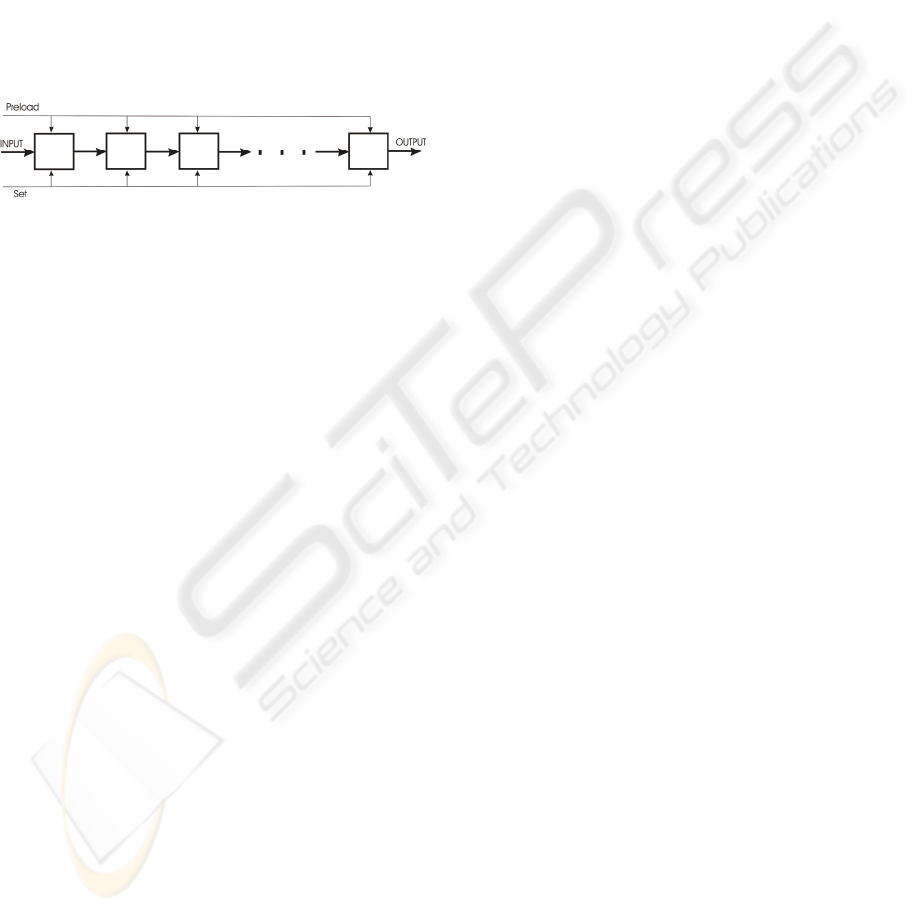
3 PROGRAMMING
The dynamically reconfigurable device would not be
functional without the possibility of programming.
The functional blocks and switching networks have
a variable component which can be programmed.
The programming is done through a series of
program blocks, connected into a chain. The exit
from one block is connected to the entry to another.
Once we are in the programming mode, a shift of the
data in the program chain occurs with each clock. In
order to program the whole device, we have to spend
as many clocks as there are blocks. The Figure 3.
represents a program chain.
Figure 3: Programming chain.
The size of the program which is to be
programmed depends on the size of the
reconfigurable device. The 8x8 element matrix
requires 64 functional units and 64 switching
networks, while programming of such a block
requires 128 programming words. In order not to
waste the time required for programming, one more
register is added to the program block. This register
is called the preload register for configuration
loading. The real program chain consists of such
preload registers. When the whole configuration is
loaded into the program series for a certain clock,
the configuration of the whole device changes so
that the data from the preload register is transferred
into the configuration register. Thereby, the function
of the device will seemingly have changed within a
single clock. While the configuration loading into
the preload registers is in progress, the
reconfigurable component can perform its current
function without being hindered by the loading of
the new configuration.
4 COMPUTATION EXAMPLES
To demonstrate the functionality and applicability of
this type of architecture, we will analyse its
application in two examples. The first example is the
calculation of a simple function:
dcbay −×+= )( .
This example is used to explain the basic
principles of how the device functions. The
dynamically reconfigurable device consists of a
single input and a single output block, three
functional units, two adders and one multiplier. To
keep the construction simple, we will not use a
larger number of elements. First comes the adder,
then the multiplier and then the other adder. The
input block is located on the entry to the device, and
the output on the exit from the block.
The program chain corresponds to the element
layout, therefore the chain begins with the input
block, which is followed by the adder, multiplier,
adder and ends in the output block. The input block
sends the data through the dout_0 exit, parameter a,
dout_1 parameter b, dout_2 parameter c and dout_4
parameter d. In the first addition block, the value
ba
+
is calculated. After that, the result of the
ba
+
addition is routed into the multiplier, where it
is multiplied by the c parameter value. The result of
the multiplication is routed to the other adder, where
it is added the
d
−
parameter value. The result
obtained in the second adder is stored in the output
block.
The first step when programming the
reconfigurable device is setting the data route delay
in a way that the data arrival to the function blocks is
synchronised. The configuration of the multiplier
ensures that the A and B entry values are multiplied
and the scaling of results is not necessary. It is also
specified that the b parameter has to be delayed by
one clock. The delay is necessary in order to achieve
synchronisation. Since the a, b and c parameters
leave the exit block at the same time, the c parameter
reaches the multiplier before the sum of
ba + . It is
for that reason that the c parameter is purposefully
delayed by one clock. The switching matrix is
programmed so that is allows the signal in_w to
enter through the A entry of the functional unit,
while the in_s signal enters through the B entry. The
multiplication results are sent to out_s and out_n.
Finally, the second adder is configured in a way
that the B entry of the functional unit is negated and
added to the A entry value. There are no A entry
delays, while the B entry is delayed by two clocks.
The reason for the delay is the same as in
multiplying. The B entry contains the result of the
cba
×
+
)(
operation, which required two clocks.
The switching matrix will take the A parameter from
the in_i input, and the B parameter from the in s
input. The result is sent to the out_s output. The final
result and all the inter-results from every block will
come to the exit block. In order to synchronise the
final results and the intermediate results, additional
delay was added on the exit, which synchronises the
data upload into the output block.
APPLICATION OF DYNAMICALLY RECONFIGURABLE PROCESSORS IN DIGITAL SIGNAL PROCESSING
345
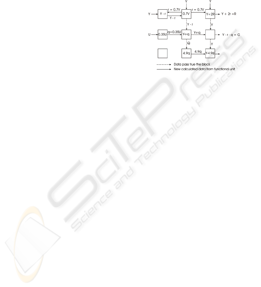
5 YUV-RGB CONVERSION
For the conversion of YUV to RGB colours, we
used the basic formation of the dynamically
reconfigurable device. The basic idea of applying
the reconfigurable device is the use of the block of
alternated
MN × functional units. Figure 4
represents such a dynamically reconfigurable device.
We used a
33× element block for the colour
conversion. The YUV to RGB conversion itself
represents the final phase of most of image and
video compression algorithms. The conversion
process is defined by the following formulas
VYR ⋅+= 4.1
VUYG ⋅−⋅−= 7.035.0 (1)
UYB ⋅−= 7.1
By introducing:
Vr ⋅= 7.0 Uq ⋅= 35.0 (2)
into the arithmetic expressions (1) we will get
r
Y
R
⋅+= 2
rqYG −−=
(3)
qYB ⋅−= 9.4
The formulas obtained in (3) were used for the
implementation of YUV-RGB conversion on a
dynamically reconfigurable device. Figure 4
represents the calculation process within the blocks.
To provide simpler orientation, we will number the
blocks by columns and rows. The first block is
marked (1,1) and the last (3,3). Let’s start from the
multiplier block (1,2), which calculates the q value
by multiplying the input value with the constant. The
result is sent to the (1,3) and (1,1) blocks. In the
(1,3) block, the q value is shifted left by one, which
corresponds the multiplication by two, and added the
Y value, resulting in the R component. In the (1,1)
block, the q value is subtracted from the Y
component and this value is sent to the (2,2) block.
In the (1,2) block, the r constant is calculated and
sent to the (2,2) block. The input values are
subtracted in the (2,2) block, resulting in
rqY −−
, which is the G component. In the (2,3)
block, the forwarded value r is multiplied by 4.9 and
the result is sent to the (3,3) block, which at one
entry has a Y and on the other
q⋅9.4
value, which,
when subtracted, results in the B component. The
conversion result is provided on exit, on every clock
with the initial delay of four clocks. The colour
conversion on a hypothetical processor according to
expressions (2) and (3) requires: Three readings
from the memory, one addition, three subtractions,
four multiplications and three memory storages. The
algorithm thus derived on a hypothetical processor
requires 14 clocks. Unlike the hypothetical
processor, the dynamically reconfigurable processor
will provide the result in a single clock with the
initial delay of four clocks. As the colour conversion
process always includes entire images, and not only
a single point, we can say that the conversion lasts
no longer than a single clock.
Figure 4: Calculation process within the blocks for YUV-
RGB colour conversion.
6 CONCLUSION
The two simple examples show that the suggested
architecture of a dynamically reconfigurable
processor can be broadly implemented in digital
signal processing systems. Instead of adding a range
of specialised devices, it is simpler and easier to use
a dynamically reconfigurable processor, which by a
simple alteration of functionality can replace several
specialised devices, thus reducing the price and
energy consumption of the whole system. We will
direct our further efforts to the improvement and
simplification of the processor architecture,
development of complex applications on such a
processor and its application in solving problems in
real systems, such as audio and video signal
decoding systems, cryptographic systems and many
others.
REFERENCES
Mlinaric H., Duracic K., Kovac M., 2005. “Dynamically
reconfigurable processor for multimedia application”,
proceedings of the 12
th
International Workshop on
Systems, Signals & Image Processing, 22-24
September 2005, Chalkida Greece.
Duracic K., Mlinaric H., Kovac M., 2003. “Optimization
methods for MPEG-4 algorithms in multimedia
application running on PDA”, EC-VIP-MC 2003, 4
th
EURASIP Conference focused on Video/Image
Processing and Multimedia Communications, 2-5 July
2003, Zagreb, Croatia.
SIGMAP 2006 - INTERNATIONAL CONFERENCE ON SIGNAL PROCESSING AND MULTIMEDIA
APPLICATIONS
346
