
RUN-TIME RECONFIGURABLE SOLUTIONS FOR ADAPTIVE
CONTROL APPLICATIONS
George Economakos
µLab, School of ECE, NTU of Athens, Iroon Polytexneiou 9, GR 15780 Athens, Greece
Christoforos Economakos
Department of Automation, Halkis Institute of Technology, GR 34400 Psachna, Evia, Greece
Sotirios Xydis
µLab, School of ECE, NTU of Athens, Iroon Polytexneiou 9, GR 15780 Athens, Greece
Keywords:
Hardware, Adaptive control, Run-time systems.
Abstract:
The requirement for short time-to-market has made FPGA devices very popular for the implementation of
general purpose electronic devices. Modern FPGA architectures offer the advantage of partial reconfiguration,
which allows an algorithm to be partially mapped into a small and fixed FPGA device that can be reconfig-
ured at run time, as the mapped application changes its requirements. Such a feature can be beneficial for
modern control applications, that may require the change of coefficients, models and control laws with respect
to external conditions. This paper presents an embedded run-time reconfigurable architecture and the corre-
sponding design methodologies that support flexibility, modularity and abstract system specification for high
performance adaptive control applications. Through experimental results it is shown that this architecture is
both technically advanced and cost effective so, it can be used in increasingly demanding application areas
like automotive control.
1 INTRODUCTION
During the last years, consumer digital devices have
been built using either application specific hardware
modules (ASICs) or general purpose software pro-
grammed microprocessors, or a combination of them.
Hardware implementations offer high speed and effi-
ciency but they are tailored for a specific set of com-
putations. If an alternative implementation is needed,
a new and expensive design process has to be per-
formed. On the contrary, software implementations
can be modified freely during the life-cycle of a de-
vice, through patches and updates. However, they are
much more inefficient in terms of speed and area.
Reconfigurable computing is intended to fill the
gap between hardware and software, achieving po-
tentially much higher performance than software,
while maintaining a higher level of flexibility than
hardware. Reconfigurable devices, including Field-
Programmable Gate Arrays (FPGAs), contain an ar-
ray of computational elements whose functionality
is determined through multiple programmable con-
figuration bits. These elements, usually called logic
blocks, are connected using a set of routing resources
that are also programmable. In this way, custom digi-
tal circuits can be mapped to the reconfigurable hard-
ware by computing the logic functions of the circuit
within the logic blocks, and using the configurable
routing to connect the blocks together to form the nec-
essary circuit. Currently, the most common config-
uration technique is to use Look-Up Tables (LUTs),
implemented with Random Access Memory (RAM).
A survey of reconfigurable devices and the underly-
ing technologies can be found in (Hartenstein, 2001).
Frequently, the areas of a program that can be ac-
celerated through the use of reconfigurable hardware
are too numerous or complex to be loaded simultane-
ously onto the available hardware. There, it is benefi-
cial to be able to swap different configurations in and
out of the reconfigurable hardware as they are needed
during program execution. This concept is known as
Run-Time Reconfiguration (RTR). RTR supports the
concept of Virtual Hardware, like the concept of vir-
tual memory offered by all modern operating systems.
Through RTR, more sections of an application can be
mapped into hardware and thus, despite reconfigura-
tion time overhead, a potential for an overall perfor-
mance improvement is provided. RTR can be applied
208
Economakos G., Economakos C. and Xydis S. (2007).
RUN-TIME RECONFIGURABLE SOLUTIONS FOR ADAPTIVE CONTROL APPLICATIONS.
In Proceedings of the Fourth International Conference on Informatics in Control, Automation and Robotics, pages 208-213
DOI: 10.5220/0001633102080213
Copyright
c
SciTePress
on different phases of the design process, accord-
ing to the granularity of the reconfigurable blocks,
which may be complex functions, simple arithmetic
and storage components or LUTs. The reconfigura-
tion data can be stored inside the reconfigurable de-
vice or transfered from an embedded or host proces-
sor.
RTR FPGAs can be used in demanding applica-
tions like modern adaptive control found in the auto-
motive industry, where a clear trend prevails today:
electronics in the vehicle are gaining more and more
significance (Javaherian et al., 2004). The number of
microcontrollers in the automobile is consistently in-
creasing. For example, luxury vehicles may have up
to 100 on-board microcontroller units in the near fu-
ture. All this functionality involve a lot of computa-
tions that can be accelerated with embedded special
purpose hardware. On the other hand, applications
like speed control need to provide solutions to a vari-
ety of problems like smooth throttle movement, zero
steady-state speed error, good speed tracking over
varying road slopes, robustness to system variations
and operating conditions and minimum controller cal-
ibrations. To achieve all these, an adaptive controller
may need to change coefficients, models and control
laws during its everyday operation which involve a lot
of reconfiguration.
This paper presents an embedded RTR architec-
ture for control applications. It is based on a mod-
ern family of FPGA devices (Xilinx Virtex 4 (Xil-
inx, 2006)) that offer many advanced reconfiguration
options. It consists of a general purpose micropro-
cessor (PowerPC), built inside the FPGA device, and
a number of reconfigurable modules. Reconfigura-
tion is done by the microprocessor through an internal
configuration port and using configuration data stored
in on-chip block RAM (BRAM). All reconfigurable
modules are small size and thus, reconfiguration time
overhead is minimal. This paper also presents the cor-
responding design methodologies that support flexi-
bility, modularity and abstract system specification.
Through experimental results it is shown that this ar-
chitecture is both technically advanced and cost ef-
fective so, it can be used in increasingly demanding
application areas like automotive control.
2 FPGA ARCHITECTURE
FPGAs are the evolution of PLAs and PLDs. They
contain pre-build programmable circuit elements and
programmable interconnects that can realize any dig-
ital system with low cost and reduced time-to-market.
The weak points of programmable logic are efficiency
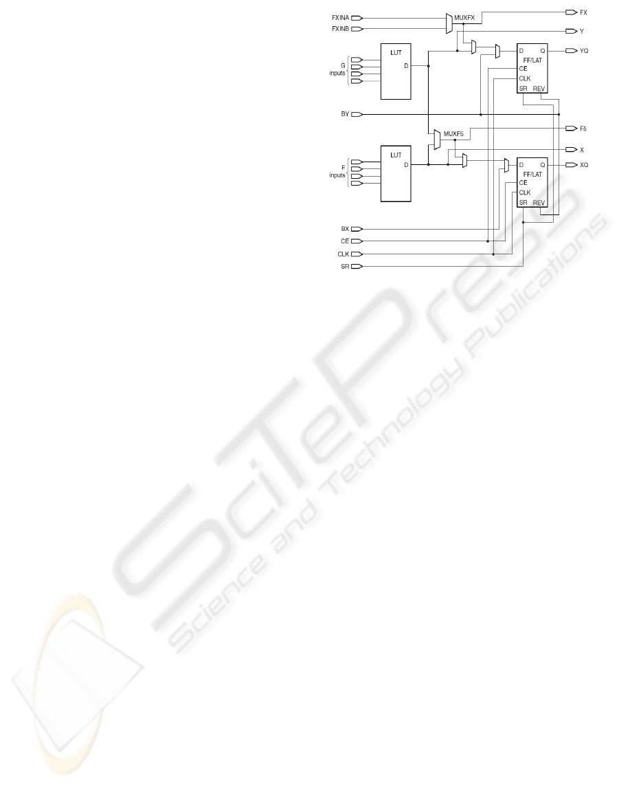
Figure 1: Simplified circuit of 2 CLB slices.
and performance but this is starting to change. A
typical FPGA device consists of programmable logic
blocks, interconnection resources and I/O blocks, ar-
ranged in an array structure.
For the devices built by Xilinx (Xilinx, 2006) the
programmable logic blocks are called Configurable
Logic Blocks (CLBs) and are divided into four slices.
Two are more powerful (called SLICEM) and two less
(called SLICEL). A simplified circuit of SLICEM is
shown in figure 1. Each slice, either in SLICEM
or SLICEL, consists of two logic-function genera-
tors or Look-Up Tables (LUTs), two storage elements,
wide-function multiplexers, carry logic, and arith-
metic gates. The extra power of SLICEM is that it
can be configured to support two additional functions:
storing data using distributed RAM and shifting data
with 16-bit registers.
LUT function generators are implemented as 4-
input RAM. There are four independent inputs for
each of the two function generators in a slice (F and
G). The function generators are capable of imple-
menting any arbitrarily defined four-input Boolean
function. The propagation delay through a LUT is
independent of the function implemented. In addition
to the basic LUTs, slices contain multiplexers that can
be used to combine up to eight function generators to
provide any function of five, six, seven, or eight inputs
in a CLB.
The other elements of the CLB may vary from
device to device. Dedicated carry logic provides
fast arithmetic addition and subtraction. The Xilinx
Virtex-4 CLB has two separate carry chains. The stor-
age elements in a each slice can be configured as ei-
RUN-TIME RECONFIGURABLE SOLUTIONS FOR ADAPTIVE CONTROL APPLICATIONS
209

ther edge-triggered D-type flip-flops or level-sensitive
latches. The D input can be driven directly by a LUT
output or by the slice inputs bypassing the function
generators, using multiplexers. Finally, the dedicated
arithmetic logic includes an XOR gate that allows a
2-bit full adder to be implemented within a slice and
an AND gate to improve the efficiency of multiplier
implementation.
The interconnection resources, called General
Routing Matrix (GRM), provides an array of config-
urable routing switches, called Programmable Switch
Matrices (PSMs), between each component. Each
CLB is tied to a PSM, allowing multiple connections.
The overall programmable interconnection is hierar-
chical and designed to support high-speed designs.
PSMs are controlled by values stored in static mem-
ory cells during configuration and can be reloaded to
change the functions of the programmable elements.
I/O blocks can be configured as inputs, outputs or
bidirectional and are connected to the GRM and to the
chip pads. They have configurable high-performance
drivers and receivers,supporting a wide variety of
standard interfaces.
FPGAs are programmed by writing a bitstream in
the configuration memory (all configuration bits and
LUT contents). The bitstream is usually externally
supplied through a serial link. For RTR, when an
application requires a change configuration memory
while the device is operational, the Xilinx Virtex-4
architecture defines the global Internal Configuration
Access Port (ICAP), which provides the user logic
with access to the configuration interface.
3 RELATED RESEARCH
Real-time embedded control is an important applica-
tion area for microelectronic devices. With the intro-
duction and wide distribution of FPGA devices a lot
of efficient hardware controller implementation have
been reported (Kim, 2000; Sanchez-Solano et al.,
2002; Chan et al., 2004; Tipsuwanporn et al., 2004;
Zhao et al., 2005). For more advanced control al-
gorithms and systems, reconfigurable solutions have
also been reported. An embedded reconfigurable ar-
chitecture is presented in (Sancho-Pradel et al., 2002),
with a number of processing elements with real-time
reconfigurable software. The main processing ele-
ment computes adaptive control coefficients in real-
time and passes them to the control processing el-
ement, which changes its software controller imple-
mentation accordingly. A more advanced multi-agent
architecture is presented in (Naji et al., 2004), which
supports hardware reconfiguration but not real-time.
In (Toscher et al., 2006) a real-time hardware recon-
figurable controller is presented. It has a number of
slots where reconfigurable modules are loaded in and
out as needed. This approach is similar to the one pre-
sented here but involves large (coarse grain) reconfig-
urable modules and so reconfiguration overhead plays
an important rope in the overall system performance.
4 DESIGN METHODOLOGY
This paper considers RTR for adaptive control appli-
cations. For small applications like a PID controller,
minor modifications are required during system oper-
ation. If an adaptive algorithm is used to generate new
coefficient values an update can replace the old val-
ues in a straightforward manner (details will be given
in a subsequent section). When however complicated
models or control laws are considered the correspond-
ing hardware design methodology has to be changed.
The solution proposed in this paper is to take the adap-
tive control algorithm of the whole system and apply
Algorithmic or High-Level Synthesis (HLS) (Gajski
et al., 1992) taking into account RTR.
HLS acts upon the dataflow graph of an applica-
tion and schedules its primitive operations in consec-
utive control steps while mapping them onto avail-
able resources. The proposed solution is a novel re-
source constrained scheduling heuristic that utilizes
RTR arithmetic units. After experimentation with dif-
ferent FPGA architectures, it has been found that a bi-
nary multiplier takes 3 to 4 times the LUTs required
for an adder of the same input bit width. So, we can
assume that we have an arithmetic component that
can be used as a multiplier in some control steps and
as 3 adders (at least) in all the others. If we per-
form resource constrained scheduling with such re-
configurable components we can reduce the latency,
in terms of control steps, of our circuit.
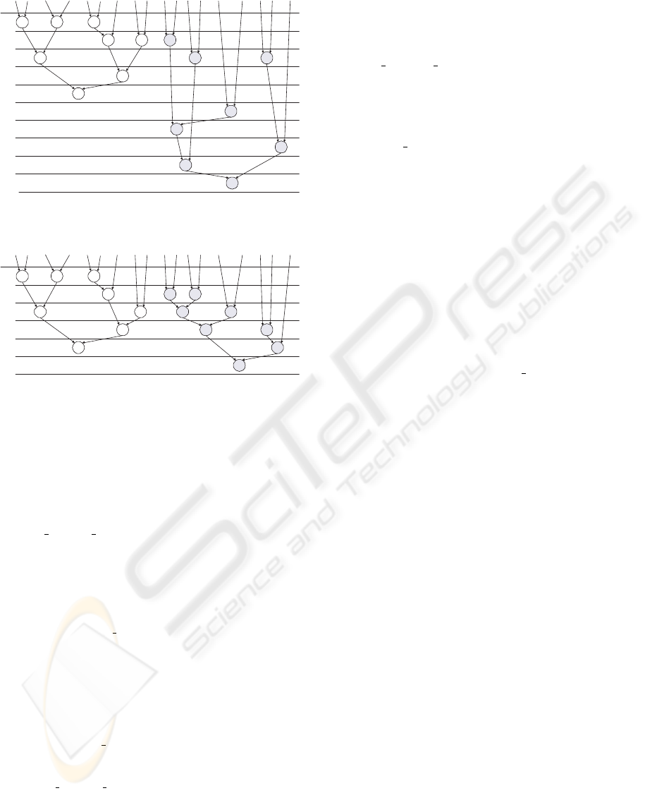
For example, consider a digital filter with two
inputs x and y and two outputs z
1
and z
2
, where
z
1
= a
0
x
0
+ x
1
+ x
2
+ a
3
x
3
+ x
4
+ a
5
x
5
and z
2
= b
0
y
0
+
b
1
y
1
+ y
2
+ y
3
+ b
4
y
4
+ y
5
. If we want to build a circuit
for this system, using two multipliers and one adder in
every control step, we will come out with the schedule
of figure 2. If one of the multipliers is reconfigurable,
and as stated in the previous paragraph can be used
as either a multiplier or 3 adders, we can reduce the
latency drastically, as shown in figure 3.
Such a result is promising taking into account that
RTR needs some time for reconfiguration at the be-
ginning of some of the control steps. To formal-
ize our approach we can modify a widely used HLS
scheduling heuristic to support RTR datapath compo-
ICINCO 2007 - International Conference on Informatics in Control, Automation and Robotics
210
x
+
+
x
x
CS=1
x
CS=2
CS=3
CS=4
x x
+
+
+
+
+
+
+
CS=5
+
CS=6
CS=7
CS=8
CS=9
CS=10
a
0
x
0
x
1
x
2
a
3
x
3
x
4
a
5
x
5
b
0
y
0
b
1
y
1
y
2
y
3
b
4
y
4
y
5
Figure 2: Schedule with 2 mult. and 1 add.
x
+
+
x
x
CS=1
x
CS=2
CS=3
CS=4
x
x
+
+
+
+
+
+
+
CS=5
+
CS=6
a
0
x
0
x
1
x
2
a
3
x
3
x
4
a
5
x
5
b
0
y
0
b
1
y
1
y
2
y
3
b
4
y
4
y
5
Figure 3: Schedule with 1 mult., 1 add. and 1 RTR mult.
nents. For resource constrained scheduling, that is,
when the number of available hardware resources is
fixed, a very efficient and widely used algorithm is
list scheduling. A modified version of list scheduling,
utilizing RTR components is shown below.
INSERT
READY OPS(V,PList
t
1
,PList
t
2
,. . .,PList
t
m
);
Cstep=0;
while ((PList
t
1
6=
/
0) or . . . or (PList
t
1
6=
/
0)) do
Cstep=Cstep+1;
for k=1 to m do
for funit=1 to N
k
do
if (PList
t
k
6=
/
0) then
S
current
=SCH
OP(S
current
,FIRST(PList
t
k
,Cstep));
PList
t
k
=DELETE(PList
t
k
,FIRST(PList
t
k
);
endif
endfor
endfor
{RPList
t
1
,. . .,RPList
t
Rn
}=MERGE(PList
t
1
,. . .,PList
t
m
);
for k=1 to Rn do
if (RPList
t
k
6=
/
0) then
S
current
=SCH
OPS(S
current
,NTH(RPList
t
k
,Cstep));
endif
endfor
INSERT
READY OPS(V,PList
t
1
,PList
t
2
,. . .,PList
t
m
);
endwhile
The algorithm uses a priority list PList for each
operation type t
k
∈ T. Each operation’s priority is de-
fined by its mobility, that is the difference between
its ALAP and its ASAP scheduling value. The op-
erations in all priority lists are scheduled into control
steps based on N
k
which is the number of functional
units performing operation of type t
k
. The function
INSERT
READY OPS scans the set of nodes V, de-
termines if any of the operations in the set are ready
(i.e., all its predecessors are scheduled), deletes each
ready node from the set V and appends it to one of
the priority lists based on its operation type. The
function SC
OP(S
current
,o
i
,s
j
) returns a new sched-
ule after scheduling the operation o
i
in control step
s
j
. The function DELETE(PList
t
k
,o
i
) deletes the in-
dicated operation o
i
from the specified list. Opera-
tions with low mobility are put first in the list. In
other words, operations that do not have many oppor-
tunities to be scheduled in subsequent control steps
are preferred for the current. As the algorithm moves
on mobilities are dynamically re-calculated. After all
available non-reconfigurable components have been
used the algorithm constructs a set of merged prior-
ity lists {RPList
t
1
,. . .,PList
t
Rn
} for each control step
with the function MERGE. Each merged list contains
ready operations that a reconfigurable component can
perform. Then, the function SCH
OPS, schedules all
operations of the same type that are in the beginning
of the merged list and cover the whole reconfigurable
component (or as much as possible). These opera-
tions are returned by the function NTH. For exam-
ple, if we have a reconfigurable component that can
perform one multiplication or three additions and the
merged priority list is {a
1
,a
2
,m
1
,a
3
,m
2
} (where a
i
de-
notes addition and m
i
multiplication), a
1
, a
2
and a
3
will be scheduled in the current control step.
The circuits designed using this heuristic are faster
but have a reconfiguration timing overhead. Depend-
ing on the implementation technology different ap-
proaches can be taken to make the final implemen-
tation efficient. In architectures with very small re-
configuration time (10ns) we can extend the duration
of every control cycle. In slower architectures we can
restrict the number of possible reconfigurations so as
the total reconfiguration delay is less than the speed
gain. Additionally, in all cases, the proposed recon-
figuration can be kept minimum by utilizing very few
(less than five) reconfigurable components.
5 EXPERIMENTAL RESULTS
The scheduling algorithm of the previous section has
been implemented on top of a custom C-to-RTL HLS
synthesis environment. In order to evaluate the pro-
posed methodology, six different DSP applications
have been used as testbenches. These applications
RUN-TIME RECONFIGURABLE SOLUTIONS FOR ADAPTIVE CONTROL APPLICATIONS
211

Table 1: DSP schedules with RTR.
Number of Number of cycles
Application nodes 3/3 2/1/2 1/1/2
Fircls 63 24 18 10
Firls 64 32 25 17
Firrcos 79 42 30 18
Invfreqz 41 25 18 10
Maxflat 115 51 38 22
Remez 55 28 20 17
were found in MATLAB’s DSP tool box and were
manually translated into untimed C (in fact SystemC)
behavioral Descriptions. The applications were Fir-
cls (Constrained least square FIR filter), Firls (Least
square linear-phase FIR filter), Firrcos (Raised co-
sine FIR filter), Invfreqz (Discrete-time filter from
frequency data) Maxflat (Generalized digital Butter-
worth filter) and Remez (Parks-McClellan optimal
FIR filter). Table 1 shows three implementations for
each application, one with 3 multipliers, 3 adders
and no reconfigurable components, one with 2 regular
multipliers, 1 reconfigurable multiplier and 2 adders
and one with 1 regular multiplier, 1 reconfigurable
multiplier and 2 adders. The implementations with
only 1 regular multiplier have an average latency im-
provement of 53% and also occupy less area. In other
words, under this approach a much better resource uti-
lization is achieved. The penalty that has to be paid
is that if reconfigurations are very frequent (for ex-
ample at the beginning of every control step) the total
reconfiguration delay may be too long. The 53% la-
tency improvement however covers even a doubling
in control step period (worst case) due to RTR.
As a more complicated example taken from car
automation we chose the detection component of the
cruise control system of (Le Beux et al., 2006). This
component compares a reference and a returned radar
signal and reports when an obstacle is found within
the next 150 m. In such situation the cruise con-
trol system should decelerated the vehicle. Compari-
son is performed with a 3 stage correlation algorithm.
Each correlation requires more than 100 multiplica-
tions. Following the same approach as the DSP ex-
periments above we found that the whole algorithm
has 472 dataflow nodes which can be arranged into
207 control steps when 4 multipliers and 4 adders are
used, 153 when 3 multipliers, 3 adders and 1 recon-
figurable multiplier is used and 98 when 2 multipliers,
2 adders and 2 reconfigurable multipliers are used.
Again the latency improvement is enough to over-
come reconfiguration delays. Practical details about
the latter are given in the next section.
6 IMPLEMENTATION ISSUES
While the proposed algorithm is focused on future ar-
chitectures with low RTR overhead, some implemen-
tation issues may be solved in an efficient way with
present and widely spread FPGA devices. Such an
issue is that if we want to have really fast reconfigura-
tion all action must be performed inside the recon-
figurable fabric, because any external source of re-
configuration data (like serial connection with a host
computer) is too slow. An answer for that prob-
lem is the Virtex family of Xilinx FPGAs, which is
equipped with an internal reconfiguration access port
(ICAP) used by internal logic to access and modify
the configuration memory. Xilinx offers a ready-to-
use IP called HWICAP (Xilinx, 2004), which can
read a portion of the configuration memory into block
RAM, modify it, and write it back, through the
ICAP port. HWICAP can be used in embedded self-
reconfigurable devices (Blodget et al., 2003; Ferreira
and Silva, 2005).
The proposed architecture is given in figure 4. The
HWICAP controller can be connected with an embed-
ded processor like PowerPC through the OPB bus (or
any bus and an OPB bridge). The processor commu-
nicates with the HWICAP controller through the bus
and requests that a part of the devices configuration
memory is written in on-chip RAM (block RAM).
Then the processor can modify this information (ac-
cessing directly block RAM) and request to be writ-
ten back. So the processor, which is initially config-
ured inside the FPGA, can reconfigure other parts of
the device during run time. To do this the processor
needs to know how to modify the copy of configura-
tion memory to achieve the required results. In our
approach, the differences between the multiplier and
the three adders can be initially stored inside Pow-
erPC (during the initial configuration phase) and ex-
changed on demand with appropriate interrupt service
routines. If the differences are kept as small as possi-
ble, this is both feasible and efficient.
This approach is called difference-based reconfig-
uration and allows fast reconfiguration of Virtex-4 de-
vices (Xilinx, 2006) at a rate of 400MB/s. The small-
est partial bitstream that the HWICAP device can han-
dle is a frame of 32 vertical slices (each slice contains
2 LUTs) which is 41 32bit words.
For our experiments we found that a 16 bit mul-
tiplier needs 54 slices while each 16 bit adder 9. In
order to minimize the reconfiguration overhead, we
used placement constraints to arrange the 3 adders
(27 slices) of the reconfigurable multiplier in a com-
mon frame. In the beginning, this frame along with
a number of neighboring slices is configured as a 16
ICINCO 2007 - International Conference on Informatics in Control, Automation and Robotics
212

PPC
ICAP
Control
Logic
HWICAP
Dual Port
Block RAM
FPGA
Cofiguration
Memory
OPB
Figure 4: Implementation architecture.
bit multiplier. When reconfiguration is needed a hard-
ware FSM generates an interrupt to PowerPC which
sends through HWICAP the frame with the 3 adders.
Also care is taken so that the reconfigurable com-
ponent has ports for all devices (both the multiplier
and the 3 adders) permanently connected to the reg-
isters and MUXs of the overall architecture. From all
these details the reconfiguration time for each recon-
figurable component can be calculated as 0.41µsec.
7 CONCLUSIONS
A novel design methodology for adaptive control
applications, which utilizes reconfigurable datapath
components has been presented in this work. Us-
ing reconfigurable multipliers, the resulting sched-
ule can be shortened so as the gain in clock cycles
can overcome the timing overhead of reconfiguration.
The main advantage of this solution is that through
RTR, more complicated algorithms can be mapped
into smaller devices without speed degradation. The
experimental results after integrating the proposed
heuristic into an HLS environment shown an average
50% reduction in clock cycles that compensates for
the worst cases of reconfiguration overhead, with bet-
ter hardware utilization. Since RTR delays will be
shortened even more in future devices, the proposed
scheduling heuristic may be proved to be even more
effective.
REFERENCES
Blodget, B., McMillan, S., and Lysaght, P. (2003). A
lightweight approach for embedded reconfiguration
of FPGAs. In Design Automation and Test in Eu-
rope Conference and Exhibition, pages 399–400.
ACM/IEEE.
Chan, Y. F., Moallem, M., and Wang, W. (2004). Efficient
implementation of PID control algorithm using FPGA
technology. In 43rd Conference on Decision and Con-
trol, pages 4885–4890. IEEE.
Ferreira, J. C. and Silva, M. M. (2005). Run-time recon-
figuration support for FPGAs with embedded CPUs:
The hardware layer. In International Parallel and
Distributed Processing Symposium, pages 165–168.
IEEE.
Gajski, D., Dutt, N., Wu, A., and Lin, S. (1992). High-Level
Synthesis. Kluwer Academic Publishers.
Hartenstein, R. (2001). A decade of reconfigurable comput-
ing: A visionary retrospective. In Design Automation
and Test in Europe Conference and Exhibition, pages
642–649. ACM/IEEE.
Javaherian, H., Liu, D., Zhang, Y., and Kovalenko, O.
(2004). Adaptive critic learning techniques for auto-
motive engine control. In American Control Confer-
ence, pages 4066–4071. IEEE.
Kim, D. (2000). An implementation of fuzzy logic con-
troller on the reconfigurable FPGA system. IEEE
Transactions on Industrial Electronics, 47(3):703–
715.
Le Beux, S., Marquet, P., Labbani, Q., and Dekeyser, J.
(2006). FPGA implementation of embedded cruise
control and anti-collision radar. In 9th Conference
on Digital System Design, pages 280–287. EUROMI-
CRO.
Naji, H. R., Wells, B. E., and Etzkorn, L. (2004). Creating
an adaptive embedded system by applying multi-agent
techniques to reconfigurable hardware. Future Gener-
ation Computer Systems, 20(6):1055–1081.
Sanchez-Solano, S., Senhadji, R., Cabrera, A., Baturone, I.,
Jimenez, C. J., and Barriga, A. (2002). Prototyping
of fuzzy logic-based controllers using standard FPGA
development boards. In 13th International Workshop
on Rapid System Prototyping, pages 25–32. IEEE.
Sancho-Pradel, D. L., Jones, S. R., and Goodall, R. M.
(2002). System on programmable chip for real-time
control implementations. In International Conference
on Field-Programmable Technology, pages 276–283.
IEEE.
Tipsuwanporn, V., Runghimmawan, T., Intajag, S., and
Krongratana, V. (2004). Fuzzy logic PID controller
based on FPGA for process control. In International
Symposium on Industrial Electronics, pages 1495–
1500. IEEE.
Toscher, S., Reinemann, T., and Kasper, R. (2006). An
adaptive FPGA-based mechatronic control system
supporting partial reconfiguration of controller func-
tionalities. In 1st NASA/ESA Conference on Adaptive
Hardware and Systems, pages 225–228. IEEE.
Xilinx (2004). OPB HWICAP Product Specification v1.3.
Xilinx (2006). Virtex-4 User Guide.
Zhao, W., Kim, B. H., Larson, A. C., and Voyles, R. M.
(2005). FPGA implementation of closed-loop con-
trol system for small-scale robot. In 12th Interna-
tional Conference on Advanced Robotics, pages 70–
77. IEEE.
RUN-TIME RECONFIGURABLE SOLUTIONS FOR ADAPTIVE CONTROL APPLICATIONS
213
