
WIRELESS TEMPERATURE SENSOR NETWORK
Wireless Sensor Data Transfer as Well as Processing
Miroslav Husak, Petr Oberreiter and Julius Foit
Department of Microelectronics, Czech Technical University in Prague, Technicka 2, CZ-166 27 Prague 6, Czech Republic
Keywords: Sensor, Wireless, Data transfer, Measurement, Control, Temperature.
Abstract: The realized system for wireless measurement of temperature in the many different places is described. The
paper describes a new architecture of a multisensor system for remote temperature measurement using
wireless communications. The system is composed of temperature sensors with digital output. The system
ensures RF wireless data transfer, wireless communication between control unit and sensors as well as
wireless switch unit. The integrated RF chip nRF9E5 ensures wireless communication. The control unit
controls communications, sensor data processing as well as switching of actuator unit. The control unit
contains main control microprocessor ATMEL as well as wireless communication unit. The actuator switch
unit communicates with control unit using RF wireless way. Partial control programmes were designed for
wireless unit control. There are many program functions implemented. The control software of the whole
system has been designed. The designed system, i.e. hardware and software has been realized and tested.
The system can operated in the range of 300 m in the free space. The number of sensor can be extensible.
The system can be use to operate with different type of sensor, i.e. for measurement other type of quantities.
PDA or mobile phone can be used to communication with control unit.
1 INTRODUCTION
Wireless transmission is very popular today for
sensor data transmission. Most RF chips are capable
to perform coding, decoding and transmitted data
synchronization at least partly, they can also feature
enhanced data security by adding CRC, parity bits
etc. These circuits perform these activities without
the need of programmed control, simplifying the
programmer’s work considerably. The RF chips are
frequently fabricated in the form of transceivers, i.e.
they include both a transmitter and a receiver in a
single package; then, the same chip can be used in
all instruments, bidirectional communication
presents no problems (Varadan, 2003). Many
producers also combine transceivers with other
circuits like A/D converters or microprocessors.
The ZigBee communication system fits well to
sensor data transmission. The standard makes
possible mutual communication of numerous
instruments over a distance of hundreds of meters. It
is distinguished by low requirements on hardware
and by extremely low power consumption. It is
described by the IEEE 802.15.4 specification.
ZigBee replaces the data transmission by RS232 or
RS485 series bus.
In our case we have used a RF module in the
Nordic technology. Its principle of operation is
similar to ZigBee. The chips operate at frequencies
433 MHz, 868 MHz, 915 MHz or 2.4 GHz.
Transmission speed is 50 kb/s and 250 kb/s in the
2.4 GHz band. In the 868 MHz band, Nordic has 7
channels, as compared with 1 channel in ZigBee, 83
channels in the 2.4 GHz band compared to 16. The
data frame is smaller, too, in addition to data it only
contains a 10-bit header, 32-bit address and a 16-bit
CRC. All chips are capable of bidirectional
operation.
The system is designed with temperature sensors.
With small adjustments, the above mentioned
principle can be used for quantities from other
energy domains (the pressure system, flow
multisensor system, humidity multisensor system,
etc.), (Kirianaki,N.V., 2002).
2 COMMUNICATION CIRCUITS
DESIGN
The communication circuit. The type nRF9E5 circuit
was selected for the communication circuits design.
The circuit contains a RF transceiver, an 8051
39
Husak M., Oberreiter P. and Foit J. (2007).
WIRELESS TEMPERATURE SENSOR NETWORK - Wireless Sensor Data Transfer as Well as Processing.
In Proceedings of the Second International Conference on Wireless Information Networks and Systems, pages 39-44
DOI: 10.5220/0002145500390044
Copyright
c
SciTePress

architecture compatible microprocessor and an AD
converter (nordicsemi, 2006).
The transceiver consists of a frequency
synthesizer, power amplifier, modulator and receiver
unit. It operates in the 433/868/915 MHz ISM bands
with adjustable frequency and output power. GFSK
(Gaussian Frequency Shift Keying) modulation is
used for the transmission, featuring a lower
bandwidth than conventional frequency modulation.
The modulation width is ±50 kHz. The data are
internally coded/decoded according to Manchester
code, resulting in 50 kb/s effective transmission
speed. The transceiver communicates with the built
in microprocessor through an internal SPI interface.
Three operating modes are available in the
transceiver: standby, transmission and reception.
The AD converter in this circuit has 4 inputs
and 10 bits. The inputs can be operated as
differential and the supply voltage can be measured
internally. Resolution can be adjusted in 4 steps
from 6 to 12 bits. The internal SPI interface is used
for A/D converter control just like the transceiver.
The circuit also has an input for AD converter
reference voltage. Alternately it is possible to use the
internal 1.22 V reference source. It is further
possible (when the external input is left free) to
measure the circuit supply voltage. In this case,
internal reference is used and 1/3 of the supply
voltage is measured. Conversion time is 8 to 14 μs,
depending on resolution.
As further hardware the circuit contains a single
channel PWM modulator, controlled by PWMCON
and PWMDUTY registers. Further the Watchdog,
Wakeup timer and low power consumption clock
pulse source. The watchdog timer is a 16 bit counter
serving to reset the microprocessor in case of an
error or endless loop in the program. The Wakeup
timer serves for interrupt or finish of some of the
economy modes. It is a 24 bit counter with
automatic fresh value recording, calling the required
operation upon reaching.
The main microprocessor. The microprocessor is
8051 architecture compatible. It includes 4 kB
program memory, 256 bytes of data memory and
special function registers. The upper 128 bits are
accessible by indirect addressing since they are
shared with special function register addresses. The
program memory is a RAM type and the program is
recorded in it by the Bootloader after SPI from the
EEPROM memory after resetting. A header must be
present in front of the program in the memory,
containing the memory speed, crystal frequency and
user data.
An ATMEL 89S8253 type was selected as the
control processor. It is a 8051 architecture
compatible microprocessor, containing additional
2 kB data EEPROM, 12 kB FLASH program
memory, SPI interface and further hardware. Both
the program and data memories are In System
Programmable (ISP), by series programming
through the included SPI interface. Further the
circuit contains a 256 byte ARM memory, whose
upper 128 bits are accessible by indirect addressing
since they are shared with SFR special function
register addresses. The lower 32 bytes of RAM are
four register banks. Instructions are fully compatible
with the 8051 architecture and operate identically
(atmel, 2006). The instruction timing is the same as
in the preceding case.
The sensors. The DS620 sensor as example can be
used for the measurement of temperature. The
circuit contains a temperature sensor, A/D converter,
comparator and a series interface. It does not need
any external components for its operation (
DS620,
2006)
. The temperature measurement range is -55
0
C
to +125
0
C. The A/D converter resolution can be
adjusted from 10 to 13 bits, corresponding to 0.5
0
C
to 0.0625
0
C resolution. The conversion duration
depends on resolution and takes between 25 ms and
200 ms. A twin lead I
2
C bus is used for
communication. The SCL terminal serves for
reception of clock pulses and the SDA terminal for
data reception or transmission. The circuit also
contains an EEPROM memory to which a part of
registers can be copied and so preserve the setting
even when the power supply is disconnected.
The real time circuit. DS1302 is a real time circuit,
counting seconds, minutes, hours, day of the week
and date including the year. For its operation the
circuit needs only an external crystal with 32768 Hz
frequency and an optional battery for continuing
function even when the primary power supply is
switched off. The circuit also contains 31 bytes of
user RAM memory, supported by the secondary
supply voltage (
DS1302, 2006).
3 SENSOR SYSTEM CONCEPT
The suggested wireless thermostat consists of
several parts. The control unit is the basic part,
securing communication with the user by means of
the display and keyboard. The unit communicates
with wireless temperature sensors and wireless
switch units. It is provided with custom-set
programs “temperature intervals”, controlling the
whole system. Second part of the system is
represented by the wireless temperature sensors. The
sensors are placed in required localities. The sensors
WINSYS 2007 - International Conference on Wireless Information Networks and Systems
40
measure temperature periodically and convey the
measured data tot the control unit. The third part is
the wireless switch units. The units communicate
with the control unit periodically and switch relays
on or off according to the measured temperatures
and values set by the user. A block schematic
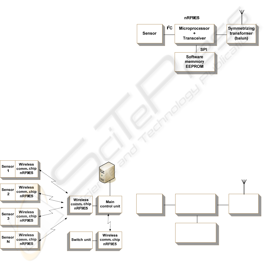
diagram of the whole system is shown in Figure 1.
The temperature sensors and switch units can be
placed at random individually and independently
according to the user’s needs. The only condition
they have to fulfill is that they must lie within the
wireless communication range. The communication
with the user is performed by means of six push
buttons and a 4 line display. Most user program
settings and settings of further parameters is dome
with the aid of a menu appearing on the display
upon pressing the appropriate button. During normal
operation, information from individual zones are
displayed periodically. They indicate the set and
measured temperature in a particular zone, sensor
and control unit battery voltage as well as an
indication of on or off state of the relay contacts.
The communication runs according the following
scheme: Before start of a transmission, each
temperature sensor or switching unit checks if
another unit is not transmitting. Then the sensor
transmits its data to the control unit and waits for
reception acknowledgement. If no acknowledgement
arrives until a certain time interval, the whole
process is repeated. When the control unit receives
data from a sensor, it first checks if it can transmit
and then sends the acknowledgement reply. The
reply to a switch unit also contains the information
on required new relay state.
Figure 1: Architecture of wireless sensor system.
3.1 Wireless Sensor Unit
Every sensor unit consists of a nRF9E wireless chip,
program memory and a symmetrical output element
- Figure 2. The input block is the temperature sensor.
The sensor used contains an AD converter and a
series interface. The communication with the
microprocessor takes place over an I
2
C bus. The
second block is the microprocessor with integrated
transceiver, processing the sensor data and
communicating with the control unit. The program
25320 EEPROM memory serves to store the
microprocessor program. The memory is connected
through the SPI series bus. The external antenna is
connected through a symmetrizing transformer
(balun).
Figure 2: Wireless sensor unit.
3.2 Wireless Switch Unit
The base of the wireless switch unit is a wireless
sensor unit, followed by the power switch part. A
block diagram is shown in Figure 3. The core is a
microprocessor with a transceiver, with program
memory connected through SPI and an antenna
connected through a balun like in the temperature
sensor. The output block is a power switch unit
controlled by two signals from the microprocessor.
The power switch device is a polarized bistable
relay. The relay is advantageous especially due to its
low power consumption (battery supply).
Power
switch unit
Microprocessor
+
Transceiver
Symmetrizing
transformer
(balun)
Software
memmory
EEPROM
nRF9E5
SPI
Figure 3: Wireless switch unit.
Its contacts remain in the “on” or “off” state without
the need for any power. Power is consumed in the
form of short pulses only, needed to change the relay
state. Contact switching is performed by connecting
a voltage of proper polarity to the relay. The relay
WIRELESS TEMPERATURE SENSOR NETWORK - Wireless Sensor Data Transfer as Well as Processing
41
selected is type G6CU-2117P-US made by OMRON
(omron, 2006). Nominal coil voltage is 3 V and the
maker guarantees correct function at 70% of
nominal voltage. The coil power consumption is
about 200 mW and minimum pulse duration for state
changeover is 200 ms.
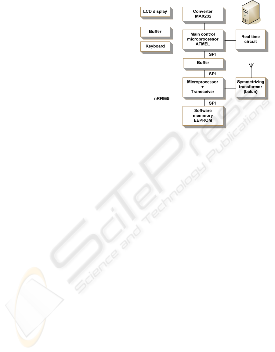
3.3 Wireless Control Unit
The block diagram of the wireless control unit is in
Figure 4. A keyboard and a display serve for
communication with the user. The keyboard uses
matrix connection and is connected to the
microprocessor through five conductors. The display
is connected by means of a buffer circuit. Four data
and four control signals serve for communication
(one microprocessor port). The main part is the
control microprocessor, t which all remaining parts
of the system are connected. The real time circuit
communicates by means of a serial bus. The bus
consists of the SCLK signal for clock frequency
transmission, the I/O signal for data and chip select
signal transmission. The transmitting and receiving
parts are very similar to those of the wireless
temperature sensor and the switch unit. The
microprocessor, memory and antenna connections
are the same, the SPI bus is used for connection with
the controlling microprocessor (MISO, MOSI, SCK
signals). The slave select signal is software on one
of the microprocessor ports. Two voltages are
needed for control unit supply, namely 3.3 V and 5
V. The 5 V supply is used for of the LCD display
and its buffer circuit. All other circuits are supplied
by the 3.3 V. A type HD4478U controller, common
with character type LCDs is used to control the
display (alldatasheet, 2006). A type AT89S8253
circuit is the core of the control unit. Since the
nRF9E5 circuit has the SPI hardware as master only,
the control processor must be operated in
slave mode.
A simple converter serves for communication
with a PC over RS232 line. It is based on a type
MAC3232 circuit. The circuit contains a doubler and
voltage inverter in addition to the RS232 line
drivers/converters (maxim, 2006).
Figure 4: Wireless control unit.
4 CONTROL SOFTWARE
Wireless temperature sensor unit control program.
The wireless sensor unit control program is based on
an endless loop, repeatedly performing the required
operations, value measurement by the sensor,
communication with the control unit, and low power
consumption waiting mode. The operation sequence
is shown in Figure 5. The circuit is waked up from
this mode by means of the Wakeup timer, set during
initialization, running in the economy mode
constantly. The wakeup period is given by the
Wakeup timer setting, in this case approximately 30
seconds. After the wakeup from the economy mode
the program run on by the next instruction
(following the instruction that caused the set on of
the economy mode), namely jumping to the start of
an endless loop and the whole process keeps
repeating. So the system is operating in the waiting
mode most of the time, with current consumption
just tens of µA, the consumption rises to
approximately 8 mA for just several hundred ms and
to about 30 mA during maximum RF power
transmission.
Wireless switch unit control program. The program
is basically similar to the preceding temperature
sensor program. The current consumption diagram
of this circuit is similar to that of the temperature
sensor. Ten of µA are consumed, increase to 6.5 mA
for 200 ms, up to 30 mA during maximum RF power
transmission and only during the relay changeover
the consumption rises to 70 mA for 250 ms. The
WINSYS 2007 - International Conference on Wireless Information Networks and Systems
42
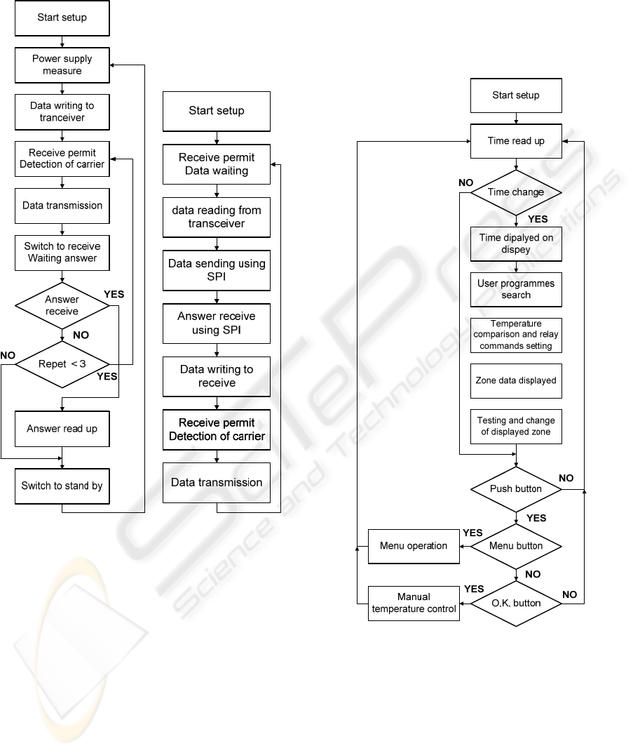
largest consumption appears during the relay
changeover, which, of course, lasts for only a short
time and the switching period is very.
Figure 5: Flow diagram of
wireless sensor unit.
Figure 6: Control
program of the wireless
transmission and
reception section of the
control unit.
Control program of the wireless transmission and
reception section of the control unit. The program
secures the control unit wireless communication
with individual sensors and switch units. Its graph is
shown in Figure 6. The program composition and its
initializing part are similar to the two preceding
programs. The transceiver is receiving most of the
time in order to be able to accept all data packets
transmitted from the other units, and only during
short intervals it transmits replies or
acknowledgements of data received from sensors or
switch units. The control unit circuit current
consumption is 13 mA and 30 mA (transmission).
Control unit program. The control program of the
Atmel processor in the control unit is the largest
program in the system. The program graph is shown
in Figure 7. The main endless loop of the program
refreshes the displayed data, evaluates and processes
data from individual zones of the memory.
Communication with the wireless part takes place
during interrupts.
Figure 7: Control unit program.
User control. There are six pushbutton provided for
the control unit handling. All stored programs can
also be listed through a PC.
5 RESULTS OF THE WORK
The programmable RF output power can be set in
four levels from -10 dBm to +10 dBm, with
corresponding communication range. The highest
WIRELESS TEMPERATURE SENSOR NETWORK - Wireless Sensor Data Transfer as Well as Processing
43
RF, output power +10 dBm, or 10 mW, means a free
space more than 300 m. The operating frequency can
also be adjusted. Setting channel number 117 means
a 868.2 MHz frequency. During tests, the system
worked flawlessly even in close presence of
common interference sources like TV receivers,
PCs, microwave ovens etc. The response time is
determined, first of all, by the wakeup period and
sensor and switch unit communication with the
control unit. The temperature measurement
resolution can be adjusted from 10 to 13 bits. This
influences the conversion time, corresponding to
about 200 ms in case of maximum resolution.
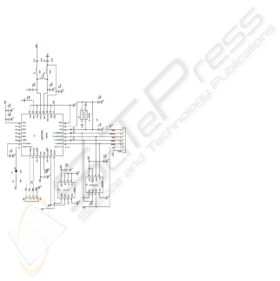
The example of the circuit connection of the
temperature sensor unit is shown in Figure 8. The
same way of the design was used in the other units.
Figure 8: Circuit connection of the temperature unit.
6 CONCLUSIONS
Research contribution of that work is design of the
sensor system with wireless data transfer. The
system can be used with minor modification in the
all energy domains for processing of physical as
well as biochemical quantities. In the work was used
example of the temperature domain. Where is made
design with other sensor type, it is necessary adjust
output parameters of the sensor to input parameters
of the wireless unit. Sensor with analog output must
used amplifier and AD converter. Wide amount of
sensors can be used for realization of the above
design system.
The system is designed like multisensor system to
be able to work with independent thermal sensors
and switch units. The reach of arrangement on of
free space is 300 m, the reach decreases in housing
development. The communication is two
bidirectional among parts of system, i.e. the data
transmission to the control unit as well as also to the
wireless sensors and switch units. Used circuit
includes also AD converter. Therefore is possible to
measure and data transfer after minority adjustments
of wireless sensors. Designed programme of control
unit occupies only part memoirs. That makes next
development of function and user's up-to-date
facilities. The program expansion is possible also in
wireless units. The control unit is patchable with
computer and one makes it possible extract user's
programmes. The cooperation with computer is
possible to extend using set-up, entry programmes or
transmission measured data to PC. The system can
be extended also alongside hardware.
ACKNOWLEDGEMENTS
This research has been supported by the research
program No. MSM6840770015 “Research of
Methods and Systems for Measurement of Physical
Quantities and Measured Data Processing” of the
CTU in Prague and partially by the Czech Science
Foundation project No. 102/06/1624 “Micro and
Nano Sensor Structures and Systems with
Embedded Intelligence”.
REFERENCES
Varadan,V.K. et al., RF MEMS and Their Applications,
Wiley, 2003.
Kirianaki,N.V.,et.al., Data Acquisition and Signal
Processing for Smart Sensors, Wiley, 2002.
http://www.nordicsemi.no, 2006.
http://www.atmel.com, 2006.
http://datasheets.maxim-ic.com/en/ds/DS620.pdf, 2006.
http://datasheets.maxim-ic.com/en/ds/DS1302.pdf, 2006.
http://downloadcentre.omron-industrial.com.
http://pdf1.alldatasheet.com, 2006.
http://datasheets.maxim-ic.com, 2006.
WINSYS 2007 - International Conference on Wireless Information Networks and Systems
44
