
NOVEL FIELD-EFFECT CONTROLLED SINGLE-WALLED
CARBON NANOTUBE NETWORK DEVICES FOR BIOMEDICAL
SENSOR APPLICATIONS
Udo Schwalke
Institute for Semiconductor Technology and Nanelectronics, Darmstadt University of Technology
Schlossgartenstrasse 8, 64289 Darmstadt, Germany
Keywords: Carbon nanotube (CNT), carbon nanotube field-effect sensor (CNTFES), carbon nanotube field-effect
transistor (CNTFET), functionalization, virus-detection, integrated circuit, CMOS, hybrid CNT-CMOS
integrated circuit, atomic force microscopy (AFM).
Abstract: In this position paper we propose a novel method for the realization of carbon nanotube field-effect sensors
(CNTFESs) which will most likely have a strong impact on the next-generation of sensors. CNTFESs are
ideally suitable for biomedical sensor applications due to their excellent inherent properties such as ultra
small size, high specific surface area and extremely high sensitivity. CNTFESs are based on carbon
nanotube field-effect transistors (CNTFETs) which are optimized for sensor applications. We have
succeeded to develop a simple, reproducible fabrication process to grow individual CNTs and CNT-
networks directly within the specified device area. No tedious manual manipulation and alignment of the
CNTs is necessary. Electrical results of the fabricated fully functional CNTFETs are presented and the use
of these devices as single-walled CNT-based field-effect controlled sensors for virus detection is discussed.
1 INTRODUCTION
Carbon nanotubes (CNTs) are hollow cylinders of
graphene with a diameter of approximately 1 nm and
lengths up to 100 µm. Multi-walled carbon
nanotubes (MWNTs) consist of several
concentrically arranged cylinders of graphene and
were observed for the first time in 1991 (Iijima
1991). MWNTs are always metallic with very good
conductivity. Single-walled carbon nanotubes
(SWNTs), however, can be either metallic (m-
SWNTs) or semiconducting (s-SWNTs) depending
on the arrangement of the carbon atoms within the
hexagonal network, i.e. their chirality.
Since 1998 (Martel 1998; Bezryadin 1998) it is
known that s-SWNTs can be used to realize carbon
nanotube field-effect transistors (CNTFETs) which
are promising candidates for future nanoelectronic
applications to replace Si-CMOS. Furthermore, only
a change in the charge state is needed to alter the
device characteristics via the field effect (i.e. just by
the presence of the charge and not via current flow),
so that extremely sensitive sensors are feasible, i.e.
carbon nanotube field-effect sensors (CNTFESs).
In addition, the inner and outer surface of the
single-walled CNT is equal to the whole tube itself
and thus the CNTFES will be extremely sensitive to
the immediate environment, i.e. ideally suited for
biomedical sensor applications. In fact, excellent
electronic response properties of CNTFETs to their
chemical (Someya 2003) and biological (Staii 2005)
environments have been demonstrated already. The
response times of CNT-sensors are at least one order
of magnitude faster than those based on solid-state
sensors. CNT-based nanosensors have the
advantages that they are thousands of times smaller
than even MEMS sensors and consume much less
power. Therefore, CNT-based nano-sensors are
highly suitable as implantable sensors. Apart from
their small size, semiconducting SWNTs operate at
room temperature with a sensitivity as high as 10
3
(Kong 2000). This enables them to perform better in
many of the biomedical sensing applications.
Currently CNTFETs and CNTFESs are
fabricated and investigated by several research
groups. However, the fabrication processes used are
often complicated, including both separate growth
(Barreiro 2006) and tedious manual manipulation of
99
Schwalke U. (2008).
NOVEL FIELD-EFFECT CONTROLLED SINGLE-WALLED CARBON NANOTUBE NETWORK DEVICES FOR BIOMEDICAL SENSOR APPLICA-
TIONS.
In Proceedings of the First International Conference on Biomedical Electronics and Devices, pages 99-102
DOI: 10.5220/0001055900990102
Copyright
c
SciTePress
the CNTs (Kong 200; Someya 2003; Staii 2005).
Obviously, commercial large scale integration
remains a major challenge to the realization of CNT-
based nanoelectronics and nanosensor technology as
well.
At our institute we have developed a novel
process to overcome the limitations of manual
fabrication of CNTFETs and hence CNTFESs as
well (Rispal 2006; Rispal 2007; Schwalke 2007).
Our group has succeeded to develop a simple,
reproducible fabrication process to grow individual
SWNTs and SWNT networks as wells in order to
fabricate fully functional CNTFETs and single-
walled CNT-based field-effect controlled sensors.
In this position paper we will first present a brief
summary of our research results on CNTFETs and
subsequently discuss the use of this technology for
possible biomedical CNT-based sensor applications.
2 RESULTS AND DISCUSSION
2.1 CNTFET & CNTFES Fabrication
The process is based on chemical-vapor-deposition
(CVD) growth of CNTs using an aluminum/nickel
‘sacrificial’ catalyst which transforms itself after
CNT growth into a high-k dielectric (i.e. Al
x
O
y
)
covered with dispersed Ni-nanoclusters (Rispal
2007). SWNTs are grown uniformly across the
wafer surface and subsequently contacted with
palladium for S/D contacts and the Si-substrate acts
as a gate electrode as illustrated in Fig. 1. The
process contains neither complicated manipulations
of the SWNTs nor multi-step lithography and is Si-
CMOS compatible. We choose the in-situ growth
method because it appears the most practical
approach for future use in high-volume fabrication
of advanced integrated nano-sensors at low cost.
For the development of this novel process we
have extensively used atomic force microscopy
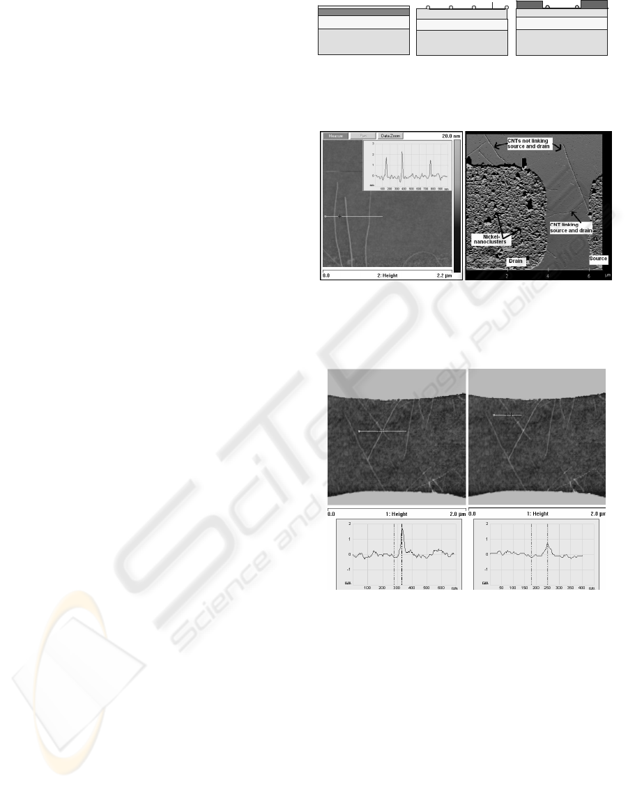
(AFM) for process control and to optimize the
CNTFET fabrication technology as well. The role of
the Al/Ni films as “sacrificial” catalyst to stimulate
SWNT growth is evident from the AFM images of
Fig. 2 where the SWNTs always start to grow from a
Ni-cluster and extend on the SiO
2
. With topographic
AFM the SWNTs with a diameter of approximately
1 - 2 nm are clearly detectable on smooth thermally
grown SiO
2
. Examples of simple CNT network
structures are shown in Fig. 3.
2.2 Electrical CNTFET Device
Characteristics
Once the electrical connection with the S/D contacts
is established, the electrical characteristics of the
CNTFETs can be obtained as shown in Fig. 4. In a
CNTFET the electric field applied via the gate
electrode modulates the charge carrier density in the
nanotube and thus the current between the source (S)
and drain (D) electrodes. Figure 4 shows the
measured drain-current (Ids) as a function of the
gate voltage (Vgs) which is swept between positive
and negative values. Our fabricated devices are fully
Si
Metal Catalyst Deposition
SiO
2
Al (8 nm)
Ni (1 nm)
Si
Metal Catalyst Deposition
SiO
2
Si
Metal Catalyst Deposition
SiO
2
Al (8 nm)
Ni (1 nm)
Si
SiO
2
AlxOy
Pd
Pd
Pd S/D Contacts (Lift-Off)
Si
SiO
2
Si
SiO
2
AlxOy
Pd
Pd
Pd S/D Contacts (Lift-Off)
(Gate)
(S) (D)
Si
SiO
2
AlxOy
Pd
Pd
Pd S/D Contacts (Lift-Off)
Si
SiO
2
Si
SiO
2
AlxOy
Pd
Pd
Pd S/D Contacts (Lift-Off)
(Gate)
(S) (D)
SWNT
Cluster Formation + CVD
Ni clusters
Si
SiO
2
AlxOy
SWNT
Cluster Formation + CVD
Ni clusters
Si
SiO
2
SiO
2
AlxOy
Si
Metal Catalyst Deposition
SiO
2
Al (8 nm)
Ni (1 nm)
Si
Metal Catalyst Deposition
SiO
2
Si
Metal Catalyst Deposition
SiO
2
Al (8 nm)
Ni (1 nm)
Si
SiO
2
AlxOy
Pd
Pd
Pd S/D Contacts (Lift-Off)
Si
SiO
2
Si
SiO
2
AlxOy
Pd
Pd
Pd S/D Contacts (Lift-Off)
(Gate)
(S) (D)
Si
SiO
2
AlxOy
Pd
Pd
Pd S/D Contacts (Lift-Off)
Si
SiO
2
Si
SiO
2
AlxOy
Pd
Pd
Pd S/D Contacts (Lift-Off)
(Gate)
(S) (D)
SWNT
Cluster Formation + CVD
Ni clusters
Si
SiO
2
AlxOy
SWNT
Cluster Formation + CVD
Ni clusters
Si
SiO
2
SiO
2
AlxOy
Figure 1: Process flow of CNTFET and CNTFES
fabrication based on CVD with sacrificial catalyst.
nmnm
Figure 2: AFM scan of SWNTs with a diameter o
f
approximately 1 to 2 nm on test structure (left). Top view
of CNTFET/CNTFES with CNT connecting source and
drain electrodes (right).
Figure 3: Example of CNT network structures with cross-
over points.
BIODEVICES 2008 - International Conference on Biomedical Electronics and Devices
100
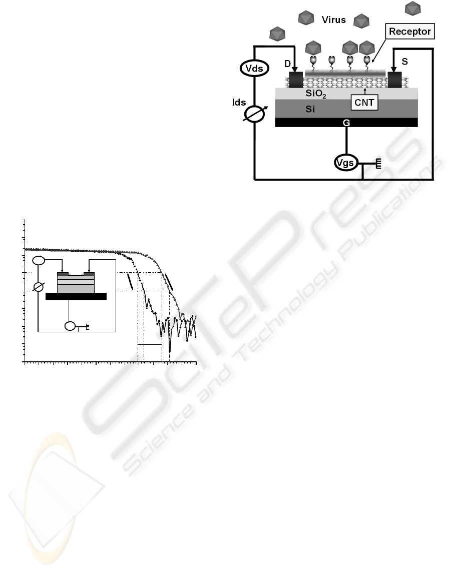
functional and the drain-current is well controlled by
the gate voltage. Similar to conventional MOSFETs,
the CNTFET device can be properly turned on and
off. In fact, the on/off current ratio is in the 10
5
range
and exceeds the values of previously published
“hand made” CNTFETs (Martel 1998; Bezryadin
1998). The transistor characteristic is unipolar and
PMOS-like, i.e. a negative gate bias is required for
turn-on.
The gate controlled drain current shown in Fig. 4
exhibits a strong hysteresis effect which is well
reproducible. It has been found (Rispal 2007) that
the hysteresis is caused by trapped charges and the
related charge transfer at the interface between the
gate dielectric and s-SWNT. With respect to CNT-
sensor applications, the hysteresis effect confirms
that any attached charges will have clearly
detectable signatures on the device characteristics of
Figure 4: Measured transfer characteristics of fabricated
CNTFET device structure. In this example the CNTFET
contains just one s-SWNT. Device characteristics of
CNTFETs containing multiple SWNTs (CNT-network)
are similar, except for the increased drain current drive
(Ids) proportional to the number of SWNTs in parallel.
CNTFETs. Since only the change in the charging
state will be needed to alter the device
characteristics via the field effect, extremely
sensitive sensors are feasible.
These CNTFET devices form the basis of the
technology platform of the proposed nano-sensors
for biomedical applications.
3 PROPOSAL: BIOMEDICAL
CNTFES
Taking advantage of the above mentioned hysteresis
effect which we observe in our CNTFET devices,
extremely sensitive nano-sensors (i.e. CNTFES)
well suitable for biomedical applications can be
realized. For example, the detection and
identification of single viral particles may be
possible using functionalized CNTFETs as sensors
as illustrated in Fig. 5: The binding of a virus to a
suitably functionalized s-SWNT will measurably
affect the gate-dependent electrical current-voltage
characteristics of the s-SWNT via charge transfer
between the CNT and the virus. The virus detection
is thus performed electronically via the CNTFET
(cf. Fig. 4) which will alter its electrical device
characteristics in presence of a virus. The sensitivity
can be enhanced further by using CNT-networks (cf.
Fig. 3) or array structures with multiple SWNTs.
Furthermore, complete electronic integrated sensor
circuits based on hybrid CNT-CMOS technology are
envisioned which will perform data analysis on-chip
(smart biosensors).
However, the main challenge for the realization
of this biomedical sensor will be the proper
functionalization of the CNT in order to be highly
selective to the desired type of virus. This
knowledge is outside of the scope of our own
-3.0 -2.5 -2.0 -1.5 -1.0 -0.5 0.0 0.5 1.0 1.5 2.0 2.5 3.0
1E-13
1E-12
1E-11
1E-10
1E-9
1E-8
1E-7
1E-6
1E-5
On-current: 210 nA
Hysteresis:
850 mV
300
mV/dec
250 mV/dec
Vds = 400 mV
SiO2 thick. = 30 nm
ABS (Ids) (A)
Vgs (V )
SiO
2
AlxOy
PdPd
Vgs
Vds
Gate
Drain Source
Ids
SiO
2
AlxOy
PdPd
SiO
2
SiO
2
AlxOy
PdPd
Vgs
Vds
Gate
Drain Source
Ids
Figure 5: Illustration of proposed CNTFET-sensor for
virus detection. The semiconducting single-walled CNT
is functionalized with a suitable receptor to allow
selective bonding via its protein. Extremely sensitive
sensors for virus detection are feasible, since any change
in the charging state introduced by the virus will alte
r
the device characteristics via the field-effect.
NOVEL FIELD-EFFECT CONTROLLED SINGLE-WALLED CARBON NANOTUBE NETWORK DEVICES FOR
BIOMEDICAL SENSOR APPLICATIONS
101

expertise (nanoelectronics). For a successful
realization of these biomedical nano-sensors
additional expertise from the biochemical and
biomedical area is needed through collaborations
with experts from the respective fields via research
projects (e.g. EU FP7). In these projects we will
provide the CNTFET-sensor devices and will be
able to perform all necessary electrical
characterization.
4 CONCLUSIONS
In this position paper we have proposed a novel
method for the fabrication of carbon nanotube field-
effect sensors (CNTFESs). These nano-sensors are
ideally suitable for biomedical sensor applications
due to their excellent inherent properties such as
ultra small size, high specific surface area and
extremely high sensitivity. Results have been
presented on the novel fabrication process to grow
individual CNTs and CNT-networks directly within
the specified device area. This is the most practical
approach for future use in high-volume fabrication
of advanced integrated nano-sensors at low cost
since tedious manual manipulations and alignment
procedures of CNTs are obsolete. As a proof of
concept electrical results on the fabricated fully
functional CNTFETs suitable for sensor applications
have been presented.
We are offering the biomedical device
community our CNT-sensor technology in order to
realize next-generation of nano-sensors within a
joint project and to evaluate their potential in
biomedical applications.
REFERENCES
Barreiro, A., et al., 2006, Applied Physics A, 82 (4), 719
Bezryadin, A., et al., 1998, Phys. Rev. Lett., 80, 4036.
Iijima, S., 1991, Nature, 354, p. 56-58
Kong, J., et al., 2000, Science 287, 622
Martel, R., et al., 1998, Appl. Phys. Lett., 73, 2447.
Rispal, L., et al. 2006, Japanese J. Appl. Physics, 45, 3672
Rispal, L., et al. 2007, International Conference on Solid
State Devices and Materials (SSDM2007), Tsukuba,
Japan.
Schwalke, U., 2007, ECS Transactions, 10, in print.
Someya, T. et al., 2003, Nano Lett. 3, 877
Staii, C., et al., 2005, Nano Lett. 5, 1774
BIODEVICES 2008 - International Conference on Biomedical Electronics and Devices
102
