
A 640 MBIT/S 32-BIT PIPELINED IMPLEMENTATION OF THE AES
ALGORITHM
Guido Marco Bertoni
1
, Luca Breveglieri
2
, Roberto Farina
3
and Francesco Regazzoni
4
1
ST Microelectronics, Agrate Briaznza, Italy
2
Politecnico di Milano, Milano, Italy
3
CEFRIEL - Politecnico di Milano, Milano, Italy
4
ALaRI, University of Lugano, Lugano, Switzerland
Keywords:
AES, Cryptographic coprocessors.
Abstract: Due to the diffusion of cryptography in real time applications, performances in cipher and decipher operations
are nowadays more important than in the past. On the other side, while facing the problem for embedded
systems, additional constraints of area and power consumption must be considered. Many optimized software
implementations, instruction set extensions and co-processors, were studied in the past with the aim to either
increase performances or to keep the cost low. This paper presents a co-processor that aims to be an inter-
mediate solution, suitable for such applications that require a throughput in the Megabit range and where the
die size is a bit relaxed as constraint. To achieve this goal, the core is designed to operate at 32 bits and the
throughput is guaranteed by a 2 stage pipeline with data forwarding. The obtained results synthesizing our
coprocessor by means of the CMOS 0.18 µm standard cell library show that the throughput reaches 640 Mbit/s
while the circuit size is of only 20 K equivalent gates.
1 INTRODUCTION
With the diffusion of cryptography in embedded ap-
plications, the need of performance started to be con-
tradictory with respect to the stricter constraints of
low power consumption and low area required by
such domain. In fact, while for high-end applications
the most important constraint is throughput, it is not
so for embedded applications which do not require
real time cryptography but instead a throughput rate
in the Megabit range. For these applications, once a
sufficient level of time performance has been reached
the constraint on time starts relaxing. As a result, it is
neither necessary nor advisable to implement in hard-
ware the whole AES round by means of a full 128-bit
architecture; a much smaller circuit can still fulfill the
time performance requirement.
Many approaches were studied in the past to ad-
dress the problems raised by the need of cryptogra-
phy in different application domains, ranging from
optimized software implementation ((Bertoni et al.,
) (Gladman, )) to instruction set extension ((Tillich
et al., 2005), (Fiskiran and Lee, 2005) (Tillich and
Grossschaedl, 2004)) and co-processor ((Feldhofer
et al., 2005) (Kuo and Verbauwhede, 2001) (Oliva
et al., 2003)). Despite this considerable amount of
previous research, only few works were addressed to
propose intermediate solutions, that target the wide
class of embedded systems, where time performance
and area are both constraints but none of them is dra-
matically strict.
In this paper, we propose a 128 bit key AES co-
processor that aims at being used in such applications
that requires to keep the silicon area reasonably low
and where acceptable time performances are needed.
The proposed coprocessor is able to perform both
AES encryption and decryption, and, in order to in-
crease its time performance, it is based on a two-stage
pipeline. Two dedicated register files are designed
to perform the ShiftRows permutation directly, more-
over, pipeline forwarding is introduced (of one data
byte only), in order to prevent stalls in the pipeline.
The remainder of this paper is organized as fol-
lows. Section 2 reviews some related work. Section 3
summarizes the Rijndael algorithm. Our proposed co-
processor for 128 bit key AES is described in Sec-
453
Marco Bertoni G., Breveglieri L., Farina R. and Regazzoni F. (2008).
A 640 MBIT/S 32-BIT PIPELINED IMPLEMENTATION OF THE AES ALGORITHM.
In Proceedings of the International Conference on Security and Cryptography, pages 453-459
DOI: 10.5220/0001925504530459
Copyright
c
SciTePress

tion 4. Experimental results and comparison with the
state of the art are reported in Section 5. Section 6
concludes the paper presenting our final remarks.
2 RELATED WORK
The initial implementations of the Rijndael algorithm
appeared soon during the AES process of the stan-
dard. Afterwards, a large number of different imple-
mentations was published, each of them targeted to
different needs.
In the previous research it is possible to find both
software and hardwareimplementations, developedin
order to meet different constraints in terms of sili-
con area, algorithm flexibility, time performance and
power consumption. Most of the research work done
in the hardware direction is related to implementation
in FPGA technology, which has substantially differ-
ent requirements and constraints with respect to the
ASIC technology. For this reason, a comparison of
our work with those related to FPGA implementation
is not possible.
An 8-bit implementation of the AES algorithm
which supports encryption and decryption is de-
scribed by Feldhofer et al. in (Feldhofer et al., 2005).
This implementation, optimized for low-resource re-
quirements, is targeted to the RFID application do-
main and is based on a 8-bit architecture. The
standard-cell implementation requires roughly 3400
equivalent gates, while the maximum clock frequency
of 80 MHz allows a data throughput rate of 9.9 Mbit
/ s.
In (Satoh et al., 2000) a compact and high-speed
architecture for 128-bit key AES is presented. Sep-
arated function blocks are developed for encryption,
decryption and key scheduling. The SubBytes trans-
formation is performed by four S-Box modules de-
signed for composite field arithmetic, which are com-
mon to the encryption round and the key schedul-
ing. Using the CMOS 0.11 µm VLSI technology, this
module can reach a throughput of 311 Mbit/s, while
the hardware complexity is of 5, 400 equivalent gates.
The architecture operates at 32 bits.
Paper (Mangard et al., 2003) presents a highly
regular and scalable AES 32-bit hardware architec-
ture, for supporting encryption, decryption, various
key sizes and the CBC mode. The architecture is a
matrix of 16 cells, which operate at 8 bits to calcu-
late the MixColumns transformation and all the other
ones, except the SubBytes. The number of S-Boxes is
customizable, and in their paper the authors show that
the highest reached throughput is 241 Mbit/s, while
the implementation requires 15 K equivalent gates.
Paper (Chodowiec and Gaj, 2003) presents a com-
pact FPGA architecture for the AES algorithm with
a key of 128 bits. Encryption, decryption and key
schedule are all implemented using limited resources.
This implementation can encrypt and decrypt data
streams of 150 Mbit / s. The architecture exploits spe-
cific features of the target FPGA, and the implemen-
tation of the MixColumns and the InvMixColumns
transformations allows to share part of the circuit be-
tween the two operations.
In (Hodjat and Verbauwhede, 2006) a high per-
formance AES processor is presented. With loop
unrolling and outer-round pipelining techniques, a
throughput of 30 Gbit / s to 70 Gbit / s is achievable
by means of a CMOS 0.18 µm VLSI technology. The
architecture proposed in the paper uses an inner round
pipelining scheme of the composite field implementa-
tion of the S-Box, and uses an off-line key scheduling.
Paper (Kuo and Verbauwhede, 2001) discusses the
architectural optimization of an AES processor. Par-
allelism and distributed memory are exploited in or-
der to reach a throughput of 1.82 Gbit / s for data
encryption. The required silicon area is of 173, 000
equivalent gates.
Paper (Hsiao et al., 2006) exposes traditional
hardware design methods and introduces a tech-
nique for area optimization. The presented Common-
Subexpression-Elimination (CSE) algorithm is ap-
plied to the subfunctions that realize the various trans-
formations in the AES encryption and decryption.
The paper claims that a cell-based implementation of
the proposed AES design can achieve an area reduc-
tion rate of about 20% with respect to using the well-
known Synopsys VLSI design tools.
A comprehensive survey can be found in (Feld-
hofer et al., ), where different hardware implementa-
tions that target various applications are presented.
3 THE ALGORITHM
In this section we give an overview of the Rijndae-
lalgorithm, that became officially AES after the pub-
lication of (Institute of Standards and Technology
(NIST), 2001), on the 26th of November 2001. As
requested by NIST, the algorithm implements a block
cipher for symmetric key cryptography and supports
a key size of 128, 192 and 256 bits, while the block
size is restricted to 128 bits. Every block is repre-
sented using four 32-bit words. The algorithm works
on a two dimensional representation of the input block
called state, which is initialized with the input data
block, holds the intermediate result during the cipher
and decipher process, and ultimately holds the final
SECRYPT 2008 - International Conference on Security and Cryptography
454
result when the process is completed. All the trans-
formations of the algorithm are grouped into a sin-
gle function called round, that is iterated a number of
times which depends on the key size.
The encryption process starts copying the input
block into the state array, and is followed by the
first key addition. In the encryption process, the
round function is composed of four different trans-
formations: ShiftRows that cyclically shifts to left the
bytes in the last three rows of the state, with dif-
ferent offsets; SubBytes that is the non-linear byte
substitution and operates independently on each byte
of the state; the MixColumns that multiplies modulo
x
4
+ 1 the columns of the state by the polynomial
{03}x
3
+ {01}x
2
+ {01}x+ {02}; and finally the Ad-
dRoundKey, that adds a round key contribute to the
state.
All the needed round keys are generated in the
AES algorithm by the so called key schedule, that
takes the secret key and executes the expansion rou-
tine as specified in the standard.
The decryption algorithm is similar to the encryp-
tion one and uses the same basic transformations, but
applied on reversed order. The decryption key sched-
ule is identical to that for encryption, but it starts us-
ing the last round key and generates the round keys in
reverse order.
4 IMPLEMENTATION
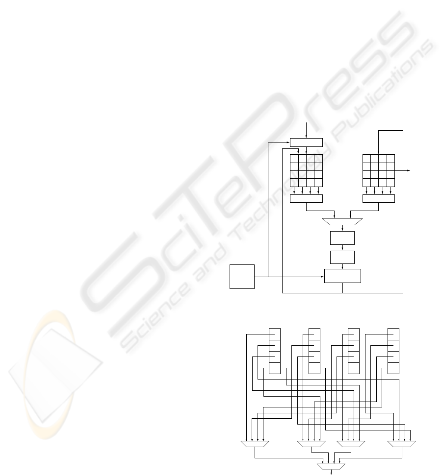
Figure 1 depicts the structure of our AES core. The
proposed accelerator has a pipeline of two stages and
is designed to compute both encryption and decryp-
tion. The state is stored in the registers by columns,
while internally each component works on words of
32 bit.
In order to avoid access conflicts, two register files
for storing the intermediate states are needed. The
second register file is also the place where the output
will be found at the end of the core computation.
The key is unrolled on-the-fly by the dedicated
module KeySched, which supports a key of 128 bits.
This is not believed to be a limitation, since most of
the hardware AES implementations nowadays sup-
ports only this key size. Furthermore, this is a dedi-
cated module, which can be modified to support other
key lengths without implications for the rest of the
core. The key addition step is performed within the
second stage of the pipeline. To allow the module to
process further blocks of data without inserting stalls
in the pipeline, a block for the key addition is inserted
uphill one of the register files: this allows computing
the first round on the next data block while complet-
ing the manipulation of the current one.
4.1 The ShiftRows Transformation
In the proposed implementation the state is stored
in the register files by columns, while the ShiftRows
transformation (and its inverse, too) operates on the
rows. In order to perform the full transformation on
a word in one clock cycle, a mechanism for retriev-
ing the bytes that the transformation is waiting for is
needed. The correct choice is performed by the selec-
tor of Figure 2: by enabling the appropriate input of
the multiplexer, each byte is loaded in the correct po-
sition for building the word needed by the next trans-
formation.
When a register file plays as input the other rep-
resents the output; in the next round, the role are
exchanged: data are written to the register file from
32 32
Selection Selection
Input
Xor round key
32
32
Output
32
32
32
32
Buffer
KeySched
32
32
ISubWord
SubWord
MixCol+XorK
XorK+IMixCol
32
Round key
Figure 1: Internal structure of the 32-bit core.
32 32 32 32
8 8 8 8 8 8 8 8 8 8 8 8 8 8 8 8
Output word
Figure 2: Byte selection for register files.
A 640 MBIT/S 32-BIT PIPELINED IMPLEMENTATION OF THE AES ALGORITHM
455
where they were read in the previous round. Because
of this, we provide both register with the same selec-
tion mechanism.
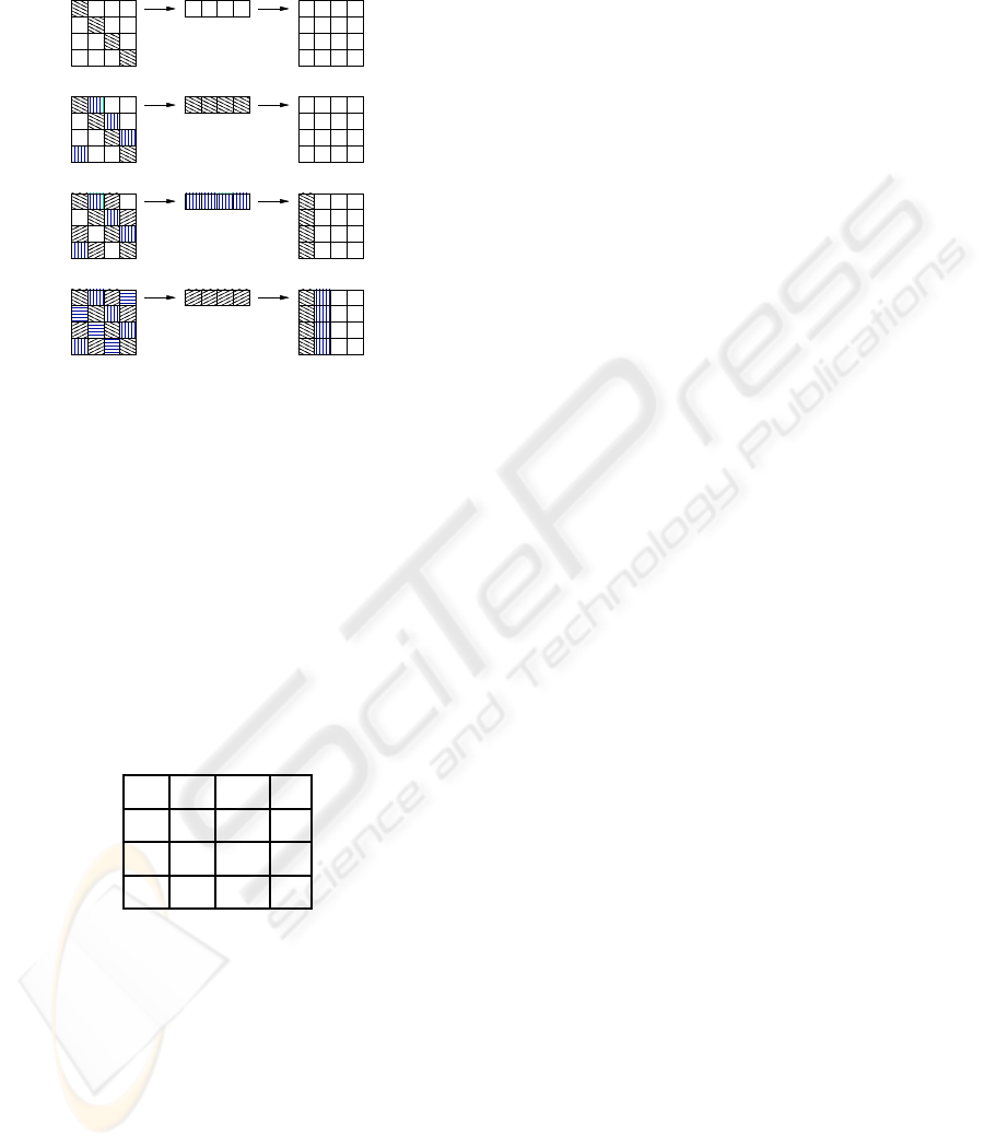
4.2 The S-Box Transformation
The SubBytes (or S-Box) transformation is performed
on a full word of 32 bits. The SubWord module is ob-
tained by combining four modules of the same kind
that perform the transformation on a byte. Differ-
ent architectures were analyzed and synthesized: in
particular one where the S-Box contents are stored in
look up tables (LUT), and one where the S-Boxes are
calculated. The final solution is presented in Figure 3:
the S-Box module performs both the direct and the in-
verse SubBytes transformation. As described in (In-
stitute of Standards and Technology (NIST), 2001),
the transformation is calculated by applying an affine
transformation over GF(2) to the multiplicative in-
verse (in GF(2
8
)) of the input. Instead, the inverse
affine transformation must be applied before taking
the multiplicative inverse. In the proposed implemen-
tation, both the Affine and the (inverse) IAffine trans-
formations are calculated, while the multiplicative in-
verse is tabulated (block Inverse of Figure 3). This
solution allows to perform both the direct and the in-
verse transformationsusing only four tables, while for
instance in the complete LUT implementation eight
tables are needed.
32
32
8 8 8 8
8888
S−box S−box S−box S−box
Output word
Input word
IAffine
Inverse
Affine
Input byte
Output byte
32
32
8 8 8 8
8888
S−box S−box S−box S−box
Output word
Input word
Figure 3: Internal structure of the SubWord module.
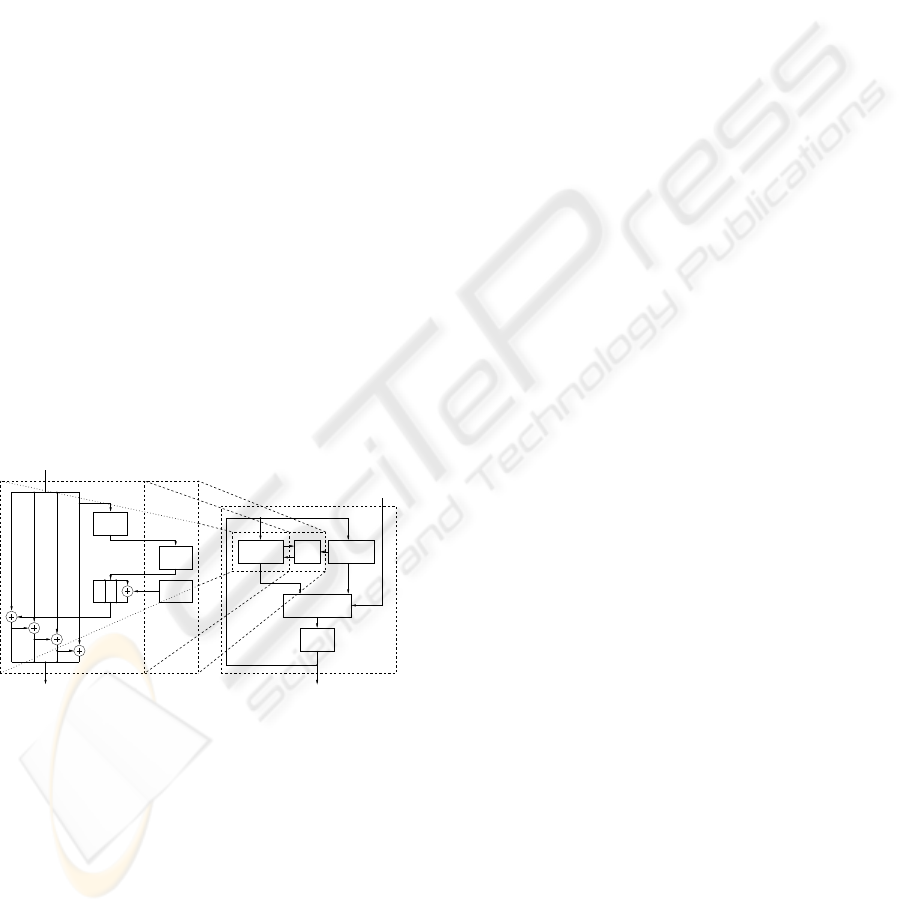
4.3 The MixColumns and Key Addition
Transformations
The module for the MixColumns transformation has
one column of the state array as input; then for ev-
ery byte the multiplied valuesare producedand xored.
In addition, the key addition step takes place and the
transformed column is output. Figure 4 overviews
the structure of the module: there are two branches,
where the direct and inverse MixColumns are calcu-
lated.
Input word
Direct
MixColumn
module
Inverse
MixColumn
module
Output word
XOR
Round Key
XOR
Round Key
Round Key
Xtime
Contributes
Addition
Contributes
Addition
IXtime
Figure 4: Overview of the MixCol module.
The XTime component is responsible for produc-
ing the different contributes of the input byte for the
direct MixColumns transformation. This component
calculates the contribute times 2 of the input byte.
By xoring this result with the initial value, the con-
tribute times 3 is obtained, while the initial value itself
represents the contribute times 1. The same mecha-
nism is applied to compute the inverse MixColumns
transformation, where the needed contributes are pro-
duced. After producing all the contributes, they must
be xored in order to obtain the transformed word: to
do so, two different sub-modules are designed. This
is why in Figure 4 two different blocks for contribute
addition are shown. Such modules are responsible
for completing the array calculations: therefore, ev-
ery component consists of four xor modules, and each
of them has four bytes as input and produces a single
byte as result.
The MixColumns module computes the key ad-
dition step too: taking advantage of its double path
structure, the key addition can be performed in the
correct sequence. Further logic is not needed because
of the difference in this step during cipher or deci-
pher operations. Since the MixColumns transforma-
tion must be skipped when computing the final round
in cipher operations and during the initial round when
deciphering, mux banks are inserted in both datap-
aths.
4.4 Key Scheduling
Figure 5 shows the module that executes the key
schedule: it produces each round key on-the-fly,
which means that every round key is computed soon
before it is used, and that after being used it is imme-
diately discarded. Such an approach has the advan-
tage of requiring less memory: in fact, the round key
can be stored in four registers, by far fewer than the
forty needed for storing the fully unrolled key. The
SECRYPT 2008 - International Conference on Security and Cryptography
456
on-the-fly method, on the other hand, must be cor-
rectly framed in the sequence of operations, in order
not to slow down the whole co-processor operation.
In the direct key scheduling, the current round key is
obtained from the round key used in the previous en-
cryption round, while for decryption the round keys
must be computed in reverse order. Therefore the key
for step (i+ 1) has to be provided to obtain the key
for step i. This implies a setup phase for decryption,
where the module calculates the last round key. After
doing so, the module works exactly in the same way
as for encryption, and therefore produces on-the-fly
the key contributes for every (inverse) round.
One small look-up table stores the values of the
round constants needed to unroll the key. Since it is
implemented as a look-up table, only one module can
be used in both cipher and decipher operations: the
control unit will produce the indexes to read the cor-
rect value.
The S-Box transformation is computed using the
tabulated modules. This solution is not the smallest
possible in terms of area requirements, but it must be
recalled that the proposed design aims to be an inter-
mediate solution, targeting applications where there
are not very strict constrains in terms of area and a
reasonable throughput is required. Because of this, to
leverage on tabulated S-Boxes for the key unrolling
represents the best possible area/performance trade
off for our target applications.
32
Secret key INPUT
3232 32
Output round key
Input round key
RotWord
SubWord
RCon
Round key OUTPUT
32
Buffer
32
Key selector
128
Direct KS Inverse KS
128
128
32
RCon
SubWord
Figure 5: Overview of the KeySched module.
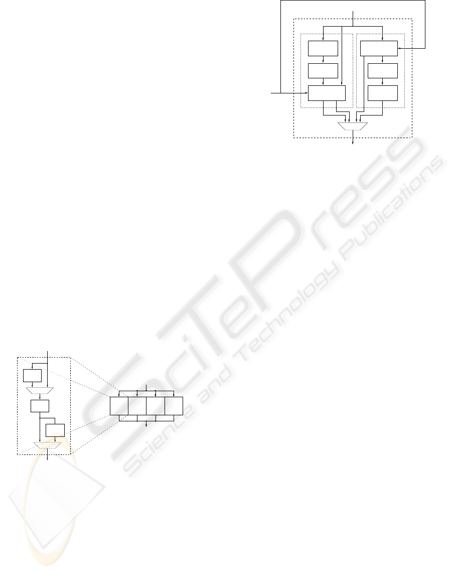
4.5 The Pipeline Stages and the
Forwarding
The first stage of the pipeline performs the ShifRows
and the S-Box transformations, using the modules de-
scribed before. The byte selection mechanisms allow
to retrieve the word to work on. The output word
is then processed by the SubWord module, which
performs the non-linear transformation of the whole
word. Two of the byte selection mechanisms must be
used in order to obtain both the direct and the inverse
ShiftRows transformations: two register files are nec-
essary, which involves a total of four byte selection
blocks. A multiplexer array will be used to propagate
the right word, depending on the operation to execute.
At the end of the S-Box module, a buffer is placed
to break the data path. At this point, the MixColumns
transformation must be executed. This transforma-
tion, however, is skipped during the last round. Con-
sequently, a multiplexer to choose to propagate the
word coming from the previous buffer instead of the
output word of the MixCol module, is inserted. Such
a function block is driven by a control unit, which
generates all the necessary control signals for the
multiplexers. This pipeline stage incorporates both
the MixColumns transformation and the key addition
step, which is performed word by word inside the
MixColumns module, too. In this way, the correct
word is directly written to the second register, com-
pleting the round.
4.5.1 The Forwarding
The top illustration in Figure 6 highlights the word
that must be read from the state array in order to
perform the ShiftRows transformation; other buffers
are initially empty. The round thus starts reading
the word [b
0
, b
5
, b
10
, b
15
], thanks to the byte selection
mechanism. This word feeds the SubWord module,
and the result is stored into the buffer at the output in
order to cut the data path. The second illustration in
Figure 6 depicts the current situation, the second word
to be read from the state array is highlighted.
In the next clock cycle, the second column,
[b
4
, b
9
, b
14
, b
3
], is read from the register file and, after
passing the SubWord module, it is stored into the in-
termediate buffer; the previous one passes through the
MixCol module, and is written into the second register
file. This produces the first column of the new state
array: the key addition step is performed inside the
MixColumns module as described in 4.3.
A further clock cycle causes the third word,
[b
8
, b
13
, b
2
, b
7
], to be read from the byte selection
blocks; this is processed by the SubWord module and
the result is stored into the buffer. The previous word
passes through the MixCol module and is stored into
the register file: the second column of the new state
array comes ready. The current situation is depicted
in Figure 6; the fourth word to be read is highlighted,
too.
Again, in the next clock cycle, the third column
passes on the MixCol module and is stored into the
register file, producing the third column of the new
state array; the fourth and last word, [b
12
, b
1
, b
6
, b
11
],
is read from the registers and passes the SubWord
A 640 MBIT/S 32-BIT PIPELINED IMPLEMENTATION OF THE AES ALGORITHM
457
module waiting for the MixColumn transformation in
the next step, as shown in Figure 6.
Buffer
Buffer
Buffer
Buffer
Figure 6: Current situation of the buffers.
In the next step the computation of the next round
must avoid inserting bubbles in the pipeline: while the
fourth word is passing through MixCol module, the
SubWord module needs to process the first column of
the newly created state array. The situation is shown
in table 1, where the “X” symbols indicate the bytes
not yet produced, and the “?” symbol underlines the
byte needed to complete the word that will become
the first one for the next round computation, consis-
tently with the adopted byte selection mechanism.
Table 1: Status matrix situation when the third word is writ-
ten.
b
′
0
b
′
4
b
′
8
X
b
′
1
b
′
5
b
′
9
X
b
′
2
b
′
6
b
′
10
X
b
′
3
b
′
7
b
′
11
?
In order to respect data dependencies, one pos-
sible solution could be the insertion of a so called
bubble into the pipeline, since when the first word
for the next round computation should be read, the
fourth word is not yet written in the register file. In
this case however,the insertion of the bubble degrades
performances, although increases the critical path. In
fact, the additional combinatorial logic needed to for-
ward the missing byte still allows to reach a higher
throughput w.r.t. the insertion of a stall in the pipeline.
Thus, if the resulting missing byte coming from the
MixCol module is forwarded directly to the SubWord
module rather than awaiting the corresponding word
to be written into the register file, the first word be-
comes ready for the next round computation during
the needed step. Note that only the last byte of such
word must be forwarded, because it is the only one
needed to complete the word to start the next round
computation, as indicated in Table 1. No problems
come from the key addition step, since key addition is
directly performed inside of the MixCol module: the
forwarded byte has been already xored with the cor-
rect key contribute.
The decryption process is similar to the encryp-
tion one, except that it requires a setup phase to com-
pletely unroll the key: this allows to retrieve the last
key contributenecessary for the reverse on-the-fly key
unrolling. During the decryption, the transformations
are applied in reverse order; no problem is raised by
the key addition step since the MixColumns module
ensures that the two datapaths correctly perform the
sequence of operations, as shown in Figure 4.
5 RESULTS
To evaluate the proposed AES coprocessor, we have
implemented it in VHDL and then synthesized with
Synopsys Design Compiler (Synopsys Design Com-
piler:, ) using a CMOS 0.18 µm standard cell library.
Our AES coprocessor works properly with a system
clock frequency up to 200 MHz, that corresponds to
a throughput of 640 Mbit/s. The required area is
250056.703125 µm
2
, which is roughly equivalent to
20 K gates (20, 329).
Table 2 shows the comparison of our implemen-
tation with the state of the art for 32 bits AES copro-
cessors. The functionalists of the above AES com-
pact coprocessors are all are identical and all of them
implement the key schedule on-the-fly. It is possi-
ble to notice that, among the compact VLSI design,
our reaches the highest throughput, which is approx-
imately twice that presented in (Satoh et al., 2000).
Silicon area is, as it could be expected, larger than
that required by the smallest solutions found in the
literature. Note however that, at best that our knowl-
edge, the reached throughput is the highest available
for AES implementation below 20 K gates, therefore,
the proposed solution is very recommendable for ap-
plications requiring Megabit throughput with reason-
able silicon area.
SECRYPT 2008 - International Conference on Security and Cryptography
458
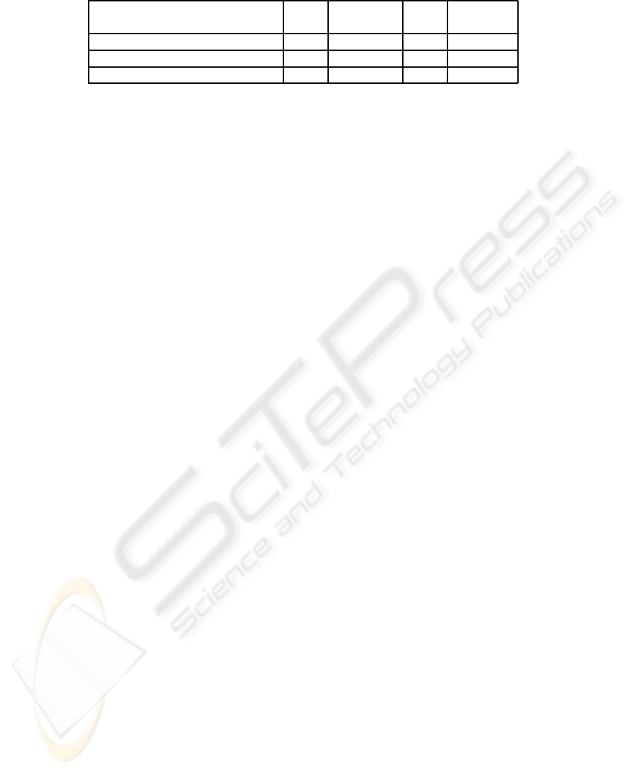
Table 2: Comparison with the state of the art: time and area.
Version Clock Throughput Area Technology
AES MHz Mbps GEs µm
Proposed 200 640 20 K 0.18
Satoh (Satoh et al., 2000) 130 311 5.4 K 0.11
Mangard (Mangard et al., 2003) 64 241 15 K 0.6
6 CONCLUSIONS
In this paper, a coprocessor for implementing the en-
cryption and decryption algorithms of the AES has
been presented. The architecture supports a key size
of 128 bits, operates at 32 bits and is based on a
pipeline of two stages with data forwarding. The
proposed coprocessor has a throughput of 640 Mbit/s
and requires approximately 20 K equivalent gates to
be implemented. The proposed AES coprocessor ex-
hibits the best time performance with respect to the
comparable ones published in the literature, at the
cost of a slightly larger area. We believe that this
implementation is particularly suitable for those ap-
plications that can not stand the cost of a 128 bits im-
plementation, but that still require a relatively high
throughput, such as in the wireless communications.
REFERENCES
Bertoni, G., Breveglieri, L., Fragneto, P., Macchetti, M.,
and Marchesin, S. Efficient Software Implementation
of AES on 32-Bit Platforms. Proceeedings of CHES
2002, 2523:159–171.
Chodowiec, P. and Gaj, K. (2003). Very Compact FPGA
Implementation of the AES Algorithm. Proceedings
of CHES 2003, pages 319–333.
Feldhofer, M., Lemke, K., Oswald, E., Standaert, F.,
Wollinger, T., and Wolkerstorfer, J. State of the art
in hardware architectures. European Network of Ex-
cellence in Cryptology, (2006).
Feldhofer, M., Wolkerstorfer, J., and Rijmen, V. (2005).
AES implementation on a grain of sand. Information
Security, IEE Proceedings, 152(1):13–20.
Fiskiran, A. M. and Lee, R. B. (2005). On-chip lookup ta-
bles for fast symmetric-key encryption. In ASAP ’05:
Proceedings of the 2005 IEEE ASAP, pages 356–363,
Washington, DC, USA. IEEE Computer Society.
Gladman, B. http://fp.gladman.plus.com/.
Hodjat, A. and Verbauwhede, I. (2006). Area-throughput
trade-offs for fully pipelined 30 to 70 Gbits/s AES
processors. IEEE Transactions on Computers,
55(4):366 – 372.
Hsiao, S., Chen, M., and Tu, C. (2006). Memory-free low-
cost designs of advanced encryption standard using
common subexpression elimination for sub-functions
in transformations. IEEETransactions on Circuits and
Systems I, 53(3):615–626.
Institute of Standards, N. and Technology (NIST) (2001).
Announcing the Advanced Encryption Standard
(AES). Federal Information Processing Standards
Publication 197.
Kuo, H. and Verbauwhede, I. (2001). Architectural Opti-
mization for a 1.82 Gbits/sec VLSI Implementation of
the AES Rijndael Algorithm. Proceedings of CHES,
pages 51–64.
Mangard, S., Aigner, M., and Dominikus, S. (2003). A
Highly Regular and Scalable AES Hardware Archi-
tecture. IEEE Transactions on Computers, 52(4):483–
491.
Oliva, D., Buchty, R., and Heintze, N. (2003). AES and the
cryptonite crypto processor. In CASES ’03: Proceed-
ings of the 2003 international conference on Compil-
ers, architecture and synthesis for embedded systems,
pages 198–209, New York, NY, USA. ACM Press.
Satoh, A., Morioka, S., Takano, K., and Munetoh, S. (2000).
A Compact Rijndael Hardware Architecture with S-
Box Optimization. In Proceedings of ASIACRYPT
2001, number 2248 in LNCS, pages 239–254.
Synopsys Design Compiler:.
http://www.synopsys.com/products/logic
.
Tillich, S. and Grossschaedl, J. (2004). Accelerating AES
Using Instruction Set Extensions for Elliptic curve
Cryptography. In LNCS 3481: Proceedings of the
Computational Science and Its Applications, pages
665–675, Berlin, Germany. Springer Verlag.
Tillich, S., Grossschdl, J., and Szekely, A. (2005). An In-
struction Set Extension for Fast and Memory-efficient
AES Implementation. In CMS 2005:Proceedings of
the Communications and Multimedia Security, pages
11–21, Berlin, Germany. Springer Verlag.
A 640 MBIT/S 32-BIT PIPELINED IMPLEMENTATION OF THE AES ALGORITHM
459
