
DEVICE FOR SYNCHRONIZED ROTATION
Shuh Jing Ying, Rufael Berhane and Rajiv Dubey
Department of Mechanical Engineering
University of South Florida
Tampa, Florida, U.S.A.
Keywords: Synchronization, Synchronized rotation.
Abstract: This device makes two shafts rotating in synchronized angular displacement. The sensors are potentiometers.
The device is designed for use in a driving simulator. The first shaft is connected to a steering wheel and
controlled by a driver so this shaft is the master, the second shaft is connected to the computer software that
displays the surrounding sceneries, therefore this shaft is the follower. The two shafts must be rotated in
synchronized mode and accurately. Major components in this device are operational amplifiers, NAND
gates, power MOFET and relays. Details in design and manufacturing are reported in this paper. This device
may be used for any place that requires two shafts rotating synchronically.
1 INTRODUCTION
Electronic Mobility Control Co.(EMC) developed an
Advanced Electronic Vehicle Interface Technology
(AVEIT) that converted the steering wheel, gas
pedal and brake pedal in a car into one joystick.
Based on the EMC system, we are building a driving
simulator for training disabled person to drive by
using a joystick for gas, brake and steering. The
forward movement of joystick is for gas pedal,
backward for brake, and right and left for steering.
However it is really difficulty for a person to drive a
real car without going through a simulator. A
simulator to be built is similar to an airplane
simulator for training pilot to drive an airplane. But
it is not so simple to build a driving simulator, many
man powers are required to work on the project from
design, computer software, and manufacturing.
Because of the limited man power and financial
resources, we bought a regular car simulator from
Simulator Systems International (SSI). It has three
screens to show the surrounding sceneries for the
driver to see. We hope to build a device that can
make EMC and SSI systems working
simultaneously. That is the whole purpose of this
project.
There are two possibilities for reaching the
synchronized rotation, mechanical and electrical
devices. After a length consideration the final
decision was on electrical approach.
Once electrical device is chosen we looked into
existing literature but to our surprise we could not
find any in our library or any nearby libraries.
Although we were pretty certain that synchronized
motors have been used in large airplanes but no
information is found. Anyway the existing device
may not fit what we need.
So we start to design a circuit for our purpose
and we build the device exactly as we want. The
details are given in this paper. After the device is
completed certainly we had quite extensive test to
check out every part. However we have not reached
to the point to train a disabled person actually to
drive.
2 DESIGN OF THE CIRCUIT
The circuit required is to operate a motor which has
enough power to rotate the steering mechanism of
the SSI system. The directions of rotation can be
clockwise and counterclockwise. The size of motor
is chosen to be similar to the servomotor used in the
EMC system. The input power of the motor is 93
watts with torque of 8.7 n-m. The motor is a geared
DC motor. Because there is no precise position
required in the operation analogue circuit is chosen
in the design. Potentiometers are used for the
position indicators and relays are used for the
control of the motor.
339
Ying S., Berhane R. and Dubey R. (2009).
DEVICE FOR SYNCHRONIZED ROTATION.
In Proceedings of the International Conference on Biomedical Electronics and Devices, pages 339-342
DOI: 10.5220/0001431903390342
Copyright
c
SciTePress

2.1 Differential Amplifier
The difference of the voltage signals from the
potentiometers are to be amplified. Positive signal
will make the motor to rotate in one direction and
negative signal then will rotate in the other direction.
A bipolar op amp, AD706, is chosen to build a
differential amplifier. The schematic circuit diagram
is shown below.
It will be idea if the amplifier is very sensitive to
the input voltage and the dissipation power is not
very large as compared to the motor power. The
output voltage is given by
()
4
#1 #2
3
14 23
1
out in in
R
VVV
R
for R R and R R
⎡⎤
=− +
⎢⎥
⎣⎦
==
Figure 1: Differential Amplifier.
See Ref. 3 for details. The specification of AD706 is
given in Appendix.
2.2 NAND Gate
Because the output voltage of AD706 is not high
enough to turn on the power MOSFET to operate the
relay, a NAND gate is used to further amplify the
positive signal. NTC4011B is chosen for achieving
this purpose. NTC 4011B is a 2 input positive logic
NAND gate. There are four NAND gates in one IC.
The specification of NTE4011B is given in
Appendix. One input of the first NAND gate is
connected to a fixed positive voltage, hence only
positive signal will go through the first NAND gate.
Two of the 4 NAND gates are used for amplifying
the positive signals when the output of AD706 is
positive. However when the output of AD706 is
negative we must lead the signal to go to other
branch and to make the motor to turn in another
direction. A negative latch is used for that purpose.
2.3 Negative Latch
A negative latch is a resetable memory block. The
output goes to high as soon as the input signal goes
to negative. This is exactly we need for the output of
AD706 goes to negative.
Two NAND gates are needed. The circuit
diagram is given as follows
Figure 2: Negative Latch.
2.4 Power MOSFET
A power MOSFET is a specific type of Metal Oxide
Semiconductor Field-Effect Transistor. It is
designed to handle large power. IRFP250N is
chosen for this circuit. When the voltage applied to
G reaches 12 v, the switch is turned on from S to D.
The specification of IRFP250N is given in appendix.
2.5 The Circuit Diagram
With some details given above, the whole circuit can
be presented as shown in Fig 3. The input signals are
from the potentiometers, one is connected to the
EMC system and one is with SSI system. These
signals go through the differential amplifier AD706.
When the difference is positive, the signal goes
through the upper branch in the circuit diagram
because one of the inputs in the NAND gate TC4011
is set to +5Vdc. This positive signal then turn on the
power MOSFET and make the motor to rotate. As
the output of AD706 is negative, the signal triggers
the negative latch and the power MOSFET in the
lower branch in the diagram is turned on
consequently the motor is turning in the another
direction.
However, when the circuit was tested, the motor
will rotate back and forth as the input difference of
AD706 is nearly zero. This will severely shorten the
life of the motor. The power supplies in the circuit
are using voltage dividers. This is only for the
saving of space in the device.
Also we experienced the lives of IC’s are very
sensitive to the voltages applied. Follow the
specifications carefully, is very important. That is
why all the specification are attached in appendix.
BIODEVICES 2009 - International Conference on Biomedical Electronics and Devices
340
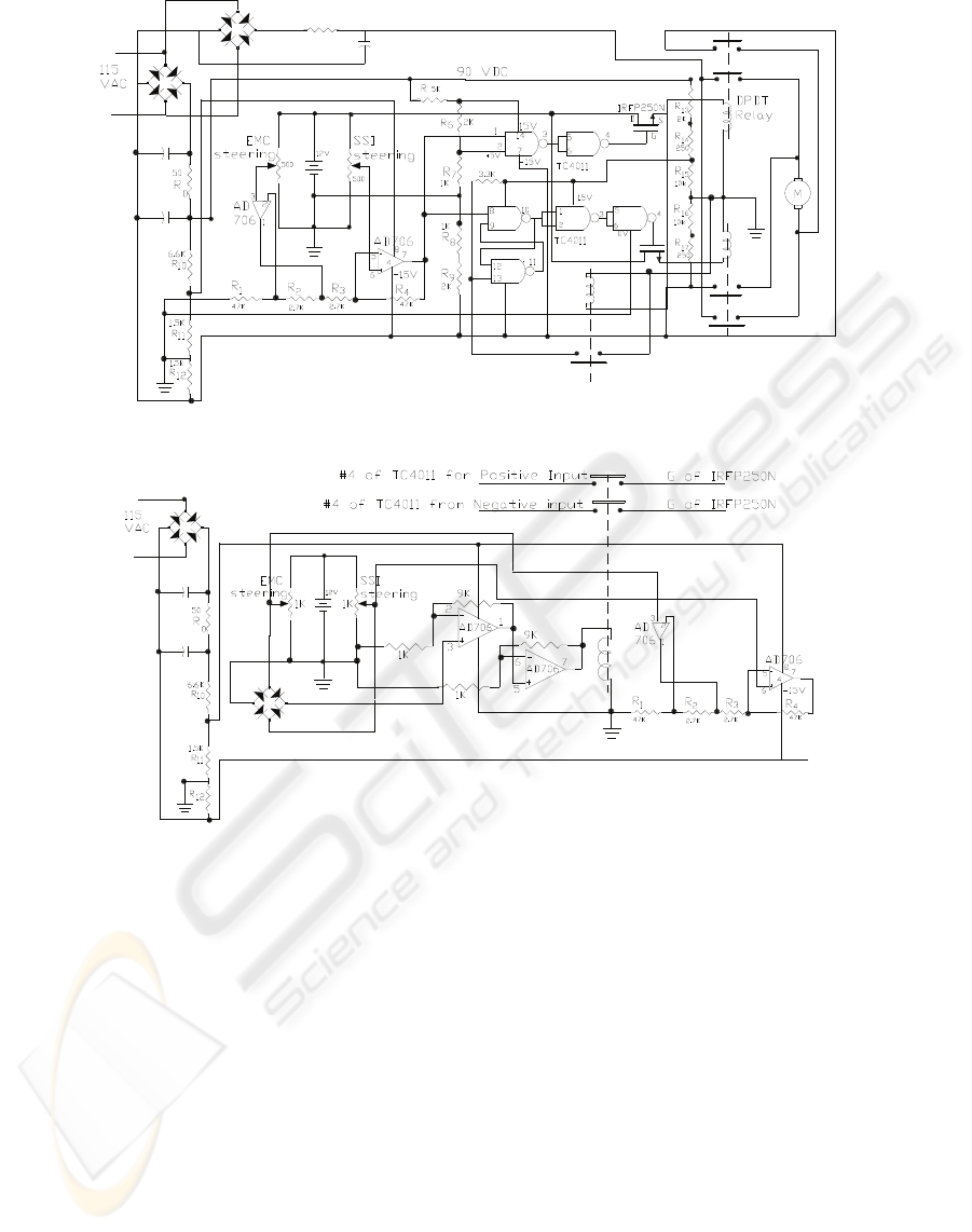
Figure 3: Circuit Diagram for Synchronized Rotation.
Figure 4: Modified Input Circuit.
2.6 Modified Input Circuit
To stop the rotation of the motor as the input of
AD706 is nearly zero. The outputs of NAND gates
and the inputs of the power MOSFETs are
disconnected The connection of these wires are
controlled by this modified input circuit that is
shown in Fig 4. Note that in this circuit the input to
IC AD706 is through a full wave rectifier. When the
signal is nearly zero, the voltage is not strong
enough to trigger the relay in this circuit so that the
relay in the previous diagram will not be turned on.
Consequently the motor will not be turned on. Now
as the EMC steering wheel rotates approximately
45
o
, the motor will start to rotate in the same
direction. And the motor will stop as the difference
between the potentiometers is within 45
o
. This
operation is considered as perfect.
3 CONCLUSIONS
Although this device is aimed originally for the use
of the synchronized rotation in a driving simulator,
actually it can be used in many other places
requiring a synchronized rotation. Because of this,
the information presented here could be invaluable
to many research workers in this community. On the
other hand this circuit is rather simple and easy to
follow, mechanical engineers can use it. The device
has been tested extensively in the simulator and it is
working perfectly well. However, the simulator has
not been used for training disabled person to drive.
This is considered as the next phase of our work.
Just to make the information completely presented.
The specifications of IC’s are given in appendix.
DEVICE FOR SYNCHRONIZED ROTATION
341

REFERENCES
Narsingh Deo, 1983, System Simulation with Digital
Computer, Prentice-Hall Englewood Cliffs, N. J.
Geert Van der Plas, Georges Gielen and Willy Sansen,
2002, A computer-aided design and synthesis for
Analog Integrated Circuits, Kluwer Academic
Publishers, Boston, MA.
Amplifier Reference Manual, 1992, Analog Devices
Norwood, MA.
The ARRL Handbook for radio 2006, 2005 83
rd
Edition A.
R. R. L.
Ying, Shuh Jing, Patti Barrett, and Stephen Sundarrao,
2008, A Device Turning on Strobe Light from Horn
Signal, BMES Annual Fall Meeting, St.Louis, MO
Ying, Shuh Jing and Stephen Sundarrao, 2007 Design and
Manufacturing of A Wheel Chair Treadmill, RESNA
2007
APPENDIX
AD706 – SPECIFICATIONS
Features:
High DC precision.
100µV max offset voltage
1.5 µV/
o
C max offset drift
200 pA max input bias current
0.5 µV p-p voltage noise, 0.1 Hz to 10 Hz
750 µA supply current
Maximum Ratings:
Supply Voltage………………………….…....…18V
Internal Power Dissipation
(Total: Both Amplifiers)……...….650mW
Input Voltage…….………………..……...….…....V
s
Differential Input Voltage…….….……….....…0.7V
Output Short Circuit Duration……….........Indefinite
Storage Temperature Range……...….-65
o
to +125
o
C
Operating Temperature Range
AD706J……….………….…........…0 to +70
o
C
AD706A…………….……….…...-40 to +85
o
C
Lead Temperature(Soldering 10sec).…….......300
o
C
Notes:
Stresses above the maximum ratings may cause
permanent damage to the device. This is a stress
rating only. Exposure to max rating conditions for
extended periods may affect device reliability. The
input pins of this amplifier are protected by back–
to–back diodes. If the differential voltage
exceeds 0.7
V, external series protection resistors should be added to
limit the input current to less than 25 mA.
TC4011-SPECIFICATIONS
The TC4011B is a quad 2 input NAND gate.
Maximum Ratings:
DC Supply voltage………….……..........…….18 V
Input voltage…….……………………….…18.5 V
Output Voltage….…………………………..18.5 V
DC input current……….……………..……..10 mA
Power dissipation…………………..……... 300 mW
Operation Temperature range………...... -40 to 85
o
C
Storage Temperature range…………… -65 to 150
o
C
IRFP250N-SPECIFICATIONS
Maximum
Ratings:
I
D,
continuous drain current…..…..……...…..… 30A
I
DM,
pulsed drain current……..….…………..…120A
Power dissipation……….…………….....………….214W
Gate to source voltage…….…………..……..……….20V
Single pulse avalanche energy………………..……315mJ
Avalanche current……..…………………..…..……..30A
Repetitive avalanche energy…….………....……….21mJ
Peak diode recovery…….………..…...…………..8.6V/ns
Operating temperature range……….....…….-55 to 175
o
C
Soldering Temperature (10 sec)……………………300
o
C
Mounting Torque…… ..….…. 1.1 N-m (10 lbf-in)
BIODEVICES 2009 - International Conference on Biomedical Electronics and Devices
342
