
AVALANCHE PHOTODIODES FOR HIGH-RESOLUTION PET
IMAGING SYSTEMS
R. Bugalho, B. Carriço, C. S. Ferreira, M. Ferreira, R. Moura, C. Ortigão
J. Pinheiro, P. Rodrigues, J. C. Silva, A. Trindade and J. Varela
1
LIP – Lab. de Instrumentação e Física Experimental de Partículas, Avenida Elias Garcia 14, 1000-149 Lisboa, Portugal
1
also at IST- Instituto Superior Técnico, Av Rovisco Pais, 1049-001 Lisboa, Portugal
Keywords: Avalanche photodiode, Dark current, Gain, Positron emission mammography, Quality control.
Abstract: A high-resolution Positron Emission Tomography (PET) scanner prototype, named Clear-PEM, was
developed by the Portuguese PET Consortium in the framework of the Crystal Clear Collaboration (CCC).
This scanner is a PET prototype dedicated for breast cancer imaging mammography, based on a novel
readout scheme constituted by fine-pitch scintillator crystals, avalanche photodiodes (APD), low-noise high-
gain frontend amplifiers and a reconfigurable FPGA-based electronics readout system. The Clear-PEM
scanner is designed to exam both the breast and the auxiliary lymph node areas, aiming at the detection of
tumours down to 2 mm in diameter. The prototype has two planar detector heads, each composed of 96
detector modules. Each detector module is composed of a matrix of 32 identical 2x2x20 mm
3
LYSO:Ce
scintillator crystals, read at both ends by Hamamatsu S8550 APD arrays (4x8) for Depth-of-Interaction
(DOI) capability. The APD arrays were characterized through the measurement of gain and dark current as a
function of bias voltage, under controlled conditions. A set of 984 APD arrays followed a well defined
quality control (QC) protocol, aiming at the rejection of arrays not complying with the defined
specifications. From the total of 984, only 1 (0.1%) was rejected, reassuring the trust in these detectors for
prototype assembly and future applications.
1 INTRODUCTION
New methods for breast cancer diagnosis are object
of heavy research efforts. One such research line
relies on the use of Positron Emission based
technology applied to breast cancer detection. In
spite of initial very encouraging results in limited
clinical trials, whole body PET systems have
considerable operational costs, with a low patient
turnover incompatible with systematic screening and
a low spatial resolution which limits the minimum
lesion size that can be detected. This has led to the
development of dedicated PET scanners, targeting
breast cancer imaging applications (Thompson et al,
1995, Moses, 2004). The PEM units are designed to
explore localized regions of the body, usually the
breast, and adopt several design principles, like fine
pixelized crystals, to achieve a better spatial
resolution, as well as a large count–rate capability.
This set of requirements has lead to the development
of a series of proof–of–principle and a few full–
assembled Positron Emission Mammography (PEM)
scanner prototypes, several of which have been used
in preliminary clinical trials, based on high density
and high–Z inorganic scintillator crystals. Of this
list, almost all lack the ability to measure the depth–
of–interaction and thus reconstructed images may
show significant aberrations due to the parallax
effect. An emerging technique to reduce this
aberration effect consists on the readout of the
scintillation light, produced in the crystal elements,
by two opposing photosensors and extracts the
coordinate of interaction along the longitudinal axis
from the asymmetry of light collection (Shao et al.,
2000). This is particular important since in a planar
detector with the active media located close to the
object under examination, the parallax effect can be
an important source of blurring in the spatial
resolution.
Several technical challenges need to be
addressed namely on how to readout the light from
the crystals without putting unacceptable amounts of
31
Bugalho R., Carriço B., S. Ferreira C., Ferreira M., Moura R., Ortigão C., Pinheiro J., Rodrigues P., C. Silva J., Trindade A. and Varela J. (2009).
AVALANCHE PHOTODIODES FOR HIGH-RESOLUTION PET IMAGING SYSTEMS.
In Proceedings of the International Conference on Biomedical Electronics and Devices, pages 31-38
DOI: 10.5220/0001432900310038
Copyright
c
SciTePress
non-active media (like conventional
photomuiltplers) between the patient port and the
crystals, which would lead to a degradation on the
final image quality and lesion detection sensitivity.
To address these issues, the Clear–PEM scanner
(Lecoq and Varela, 2002, Abreu et al, 2006), was
developed by the Portuguese PET Consortium,
composed by: Laboratório de Instrumentação e
Física Experimental de Partículas (LIP), Instituto de
Biofísica e Engenharia Biomédica da Faculdade de
Ciências de Universidade de Lisboa (IBEB),
Instituto de Biomédico de Investigação de Luz e
Imagem (IBILI), Instituto de Novas Tecnologias
(INOV), Instituto de Engenharia de Sistemas e
Computadores Investigação e Desenvolvimento
(INESC-ID), Instituto de Engenharia Mecânica e
Gestão Industrial (INEGI), Hospital Garcia da Orta
(HGO), Instituto Português de Oncologia (IPO) in
Porto and with the participation of CERN
(Organisation Européene pour la Recherche
Nucléaire) through the international collaboration
Crystal Clear Collaboration.
The detector is based on pixelized LYSO:Ce
crystals optically coupled on both extremities to
avalanche photodiodes (APD) and readout by a fast,
low-noise electronic system. The choice of
avalanche photodiodes was dictated by its
compatibility with the implementation of a double
readout technique. The APDs also demonstrate good
energy resolution for a direct detection of X-rays
and for LYSO:Ce scintillator light readout, with low
multiplication noise and acceptable gain uniformity.
The Hamamatsu S8550 APD was selected for the
Clear-PEM detector, which offers a stable working
regime up to gain 200 (Abreu et al., 2007), and has a
dark current noise below 27 electrons ENC at room
temperature (Kapusta et al., 2003).
The total number of APD arrays needed for a
single scanner is 384, and the S8550 arrays were
manufactured by Hamamatsu Photonics Inc. Japan.
A total of 984 photodetectors were acquired for
assessment.
A quality control protocol and methodology were
developed in order to assess and characterize the
acquired APDs. In this paper the adopted quality
check procedures for the APD arrays is described
and the controlled parameters are presented (gain
dependence on bias voltage, gain variation at various
voltages, dark current dependence on the bias
voltage).
2 CLEAR-PEM IMAGING
SYSTEM
2.1 Detector Heads
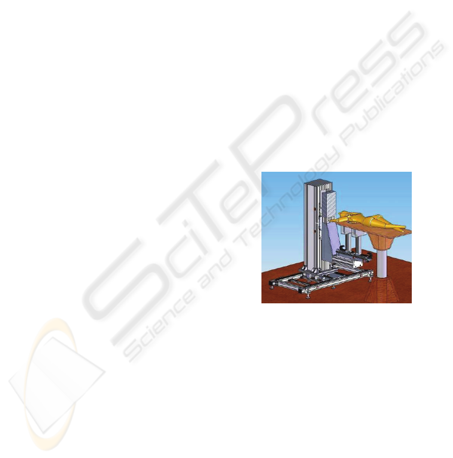
The Clear-PEM imaging system (Figure 1) is based
on a two parallel detector heads design. The detector
consists in two compact and planar detector heads
with adequate dimensions for breast and axilla
imaging. A dedicated gantry was built in order to
allow the rotation of the detector heads in breast
exams as well as to permit exams of the axilla
region. Each detector head holds the scintillator
material matrices and the frontend readout circuitry
composed of multi–pixel APD photosensors,
frontend ASIC chips, free–sampling ADCs and
Channel Link LVDS serializers. Auxiliary sub–
systems are also assembled in the detector heads,
providing environmental monitoring, cooling, power
supply and system clock distribution. A dedicated
digital trigger and data acquisition system is used for
online selection of coincidence events with high
efficiency, large bandwidth and negligible dead-time
(Albuquerque et al 2006, Albuquerque et al 2008a).
Figure 1: The Clear-PEM imaging system (CAD image).
The structure of a detector head starts in the
detector module. The detector module is composed
by the LYSO:Ce crystal matrix, optically coupled
(through an optical glue) to a S8550 APD array, on
each end, for DOI measurements. The APD array is
mounted in a small PCB with a low footprint SMT
connector on the back side. The components of the
detector module are housed and sealed in a
dedicated plastic assembly. The assembly has two
empty slots in which two detector modules can be
plug–in, defining a ”double module”. 12 detector
modules are mechanically fixed and electrically
connected to a front and back Frontend Boards
(FEBs) forming a Supermodule (Figure 2)
(Albuquerque et al, 2008b).
BIODEVICES 2009 - International Conference on Biomedical Electronics and Devices
32
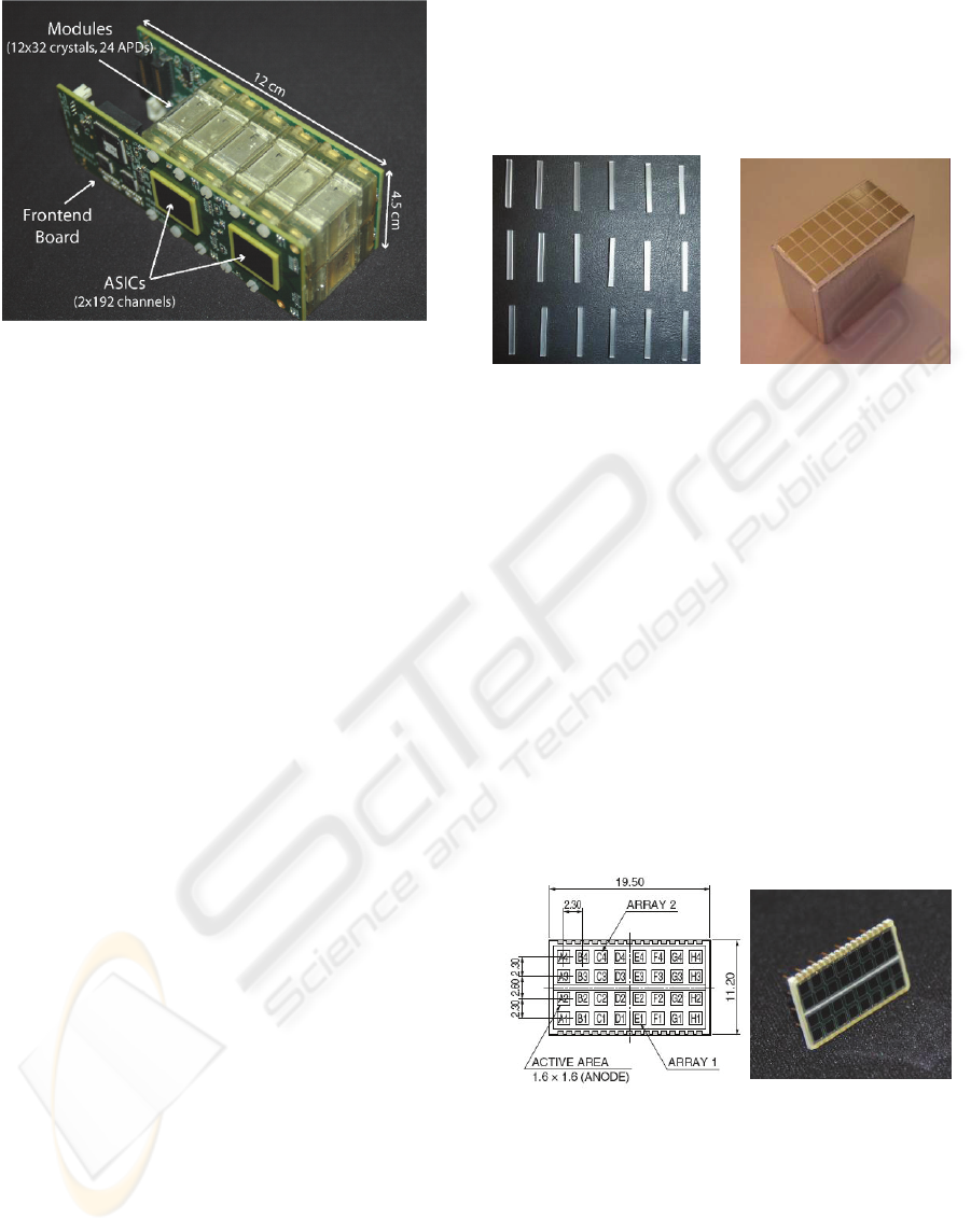
Figure 2: Supermodule structure assembling 12x32
LYSO:Ce crystals and 24 APDs in double readout. Each
Frontend board has two 192 input channels ASICs.
The assembled modules underwent a quality
control measurements carried out at LIP (Amaral et
al., 2006). The electronics chips were mounted on
the external faces of the two FEBs. Connectors for
cables linking to the data acquisition system were
also mounted in the PCBs. In a detector head, eight
Supermodules, each with 12 modules, are mounted
together.
The final prototype has two planar parallel
detector heads with 192 detector modules, 6144
crystals and 384 APD arrays (12 288 APD pixels),
covering a 17×15 cm
2
Field-of-View.
2.1.1 Crystals
The chosen scintillator for the Clear-PEM was a
inorganic crystal, LYSO:Ce. The LYSO:Ce is
cerium activated lutetium–yttrium–ortho–sylicate
(Lu
2(1−x)
Y
2x
SiO
5
:Ce) and has similar properties to
LSO:Ce (Lu
2
SiO
5
) (Melcher and Schweitzer, 1992).
The choice of this scintillator was dictated by its
high light output (27-30 photons/keV) compatible
with good energy measurements (9% at 662 keV
with a PMT readout), as well as a fast rise time and
decay (42 ns time constant) compatible with high–
quality timing measurements and low dead time. Its
peak emission is short–blue/long ultraviolet (UV)
wavelength (420 nm).
For the Clear-PEM scanner, crystals with
dimensions of 2×2×20 mm
3
were chosen. The 20
mm longitudinal size guarantees a large detection
efficiency for 511 keV photons and the
determination of the DOI coordinate with a
resolution of 2 mm (FWHM) (Abreu et al., 2006,
Amaral et al., 2006).
In total the scanner uses 6144 pixel LYSO:Ce
crystals (Figure 3a) divided in 192 matrices,
composed by a 4×8 LYSO:Ce crystal array (Figure
3b). In this configuration, the crystals are optically
isolated by 300 µm BaSO
4
reflector walls. The
BaSO
4
provide the crystal support and provides the
diffuse reflecting surfaces needed to optimize the
light collection and the DOI measurements.
Figure 3: Photograph of (a) a sample of 2×2×20 mm
3
LYSO:Ce crystals produced for the Clear-PEM scanner
and (b) an assembled BaSO
4
–type matrix.
2.1.2 Photosensors
The S8550 APD array from Hamamatsu Photonics
with a 32 pixels in an 8×4 configuration was the
selected photodetector for the Clear-PEM scanner
(Figure 4a and b). The S8550 array is assembled
from two distinct monolithic silicon wafer parts, of
2×8 ”reverse” type structure pixel elements, and
each 2x8 group is called an sub-array. The sub-array
that contains the APD pixels from A1 to H1, and
from A2 to H2, is called sub-array 1. The remaining
pixels are contained in the sub-array 2. Each sub-
array is biased independently. The pixels are
mounted on a 1 mm thick ceramic package with a
0.5 mm thick epoxy window (Kapusta et al., 2003).
Figure 4: (a) Schematic representation of the 32 pixel
Hamamatsu S8550 APD array (dimensions in millimetres)
and (b) photograph of a S8550 APD array.
Each Si pixel element has a 1.6×1.6 mm
2
,
compatible with an individual 1:1 readout of 2×2
mm
2
cross–section LYSO:Ce crystals. The element
pitch is 2.3 mm and all the pixels placed in the same
sub–matrix share the same common bias.
(a)
(b)
(a)
(b)
AVALANCHE PHOTODIODES FOR HIGH-RESOLUTION PET IMAGING SYSTEMS
33

A compilation of the Hamamatsu S8550 main
electrical and optical characteristics are present in
Table 1. The effective APD gain (ratio of the total
number of secondary avalanche electrons produced
by the initial number of electron–hole pairs due to
the scintillation light) is between 70 and 350 with a
specified inter–pixel gain variation less than 5%
r.m.s. and a dark current of 2–4 nA per pixel. The
terminal capacitance is 10 pF per pixel (Abreu et al.,
2007).
Table 1: Hamamatsu S8550 APD 32 channel electrical and
optical parameters (Abreu et al, 2007, Mosset, 2006).
Parameter Hamamatsu S8550
Pixel Size 1.6 x 1.6 mm
2
Pixel Pitch 2.3 mm
Window Type 0.5 mm epoxy resin
Peak Wavelength 600 nm
QE @ 420 nm 72-76%
Gain (M)
Gain Gradient @ M=70
Dark Current
Capacitance
50 – 350
3.6%/V
2.4 nA (pixel @ M=70)
10 pF (pixel @ M=70)
The S8550 APD operates at a bias voltage of
360-500 V, depending on the required gain. The
gain shows a temperature gradient of –2.4%/◦C at
gain 70. This is due to lattice vibrations in the silicon
structure of the APD which are enhanced as
temperature increases making more probable to
interact with avalanche secondary electrons.
Temperature drifts, if not controlled, may thus
originate gain drifts contributing to a detioration of
the energy resolution (Crespo et al., 2004,
Spanoudaki et al., 2005). The temperature gradient
is also function of the bias voltage, which means that
at higher gains the APDs show an increased
susceptibility to temperature drifts. All this imply
that the system has to operate under stable thermal
conditions. The gain gradient as function of the
polarizing bias is observed to vary as function of the
gain. For the highest gain the bias polarization
supplies must be very stable with controlled amounts
of tension ripple (Abreu et al., 2007).
2.2 Electronic Systems
The frontend and data acquisition electronics
systems are key components in the developed PET
system, enabling a high detection sensitivity and low
random background noise, without compromising
the spatial resolution, allowed by fine segmented
crystals. The data acquisition and trigger electronics
of the Clear–PEM scanner is composed by three
main blocks (Albuquerque et al., 2006):
The Frontend Electronics System, performs
signal amplification, channel selection and
analog multiplexing, analog to digital
conversion and parallel–to–serial translation;
The Trigger and Data Acquisition System,
which implements the temporary data storage,
first–level trigger (L1) computation and data
transfer to the acquisition computer (DAE
server);
The Software Trigger (L2), implemented in the
DAE server, in which the received data from
the DAE crate is un–packed, extraction
algorithms (time, energy, DOI) applied and
the trigger re–validated;
The on–detector electronics includes the
amplifier and analog multiplexing integrated circuits
(frontend ASIC). The front-end system is based in a
data-driven synchronous design that identifies and
multiplexes the analog signals of channels above
threshold, reducing the number of channels by a
factor of 96. To transmit the signals from the
detector heads, digital serializers are used to
minimize the number of lines connecting to the
trigger and data acquisition system (Rodrigues,
2007).
The off–detector system receives the serialized
digitized data streams, applies a coincidence trigger
based on the computation of the pulses amplitude
and timing, and pushes the data into the data
acquisition computer. The trigger and data
acquisition logic is implemented in large FPGAs
with 4 and 3 million gates respectively, with the
trigger algorithm decomposed in a sequence of
elementary operations executed in pipeline mode.
The system was designed to operate at a maximum
input clock frequency of 100 MHz and be able to
sustain a data acquisition rate of 1 MHz with
efficiency above 90–95%, under a maximum total
single photon background rate in the detector of 10
MHz. The communication between the readout
system and the data acquisition computer is
established through a serial high–speed link
allowing the off–detector crate to be located several
meters away from the DAE server data acquisition
computer.
2.3 Mechanical Systems
The Clear-PEM mechanical system was designed to
allow the exam of both the breast and the auxiliary
lymph nodes. The system is used in conjunction with
a shielded examination table that enables exams to
be performed with the patient kept in prone position.
Configurable openings in the examination table
BIODEVICES 2009 - International Conference on Biomedical Electronics and Devices
34
allow the exam of both breasts with the detector
heads positioned in each side of the breast (Abreu et
al., 2006). During the exam the detector heads can
rotate around the detector main axis in order to
collect data at several angular orientations as
required for tomographic reconstruction.
The examinations of the breast region close to
the chest and of the axilla region are performed in a
front-back configuration. In these exams one
detector head is facing the breast (complementary
exam), or the shoulder (axilla exam), under the
scanner table and the other is positioned against the
patient back.
3 QUALITY CONTROL OF
AVALANCHE PHOTODIODES
The scanner construction starts with the quality
control (QC) and gain characterization of all APD
arrays acquired by the PET consortium, in order to
assess which ones are useable in the final prototype.
The project commercially acquired 984 APD arrays
which needed a fast evaluation. An automatic
measuring setup was developed, based on the direct
measurement of the APD-array common cathode
current when illuminated by a blue LED light (to
simulate the LYSO:Ce scintillation). This automatic
measuring setup was named “APD Tester”. The blue
light (420 nm) from the LED is homogeneously
distributed by a light guide through all APD pixels.
The characterization consists in the measurement
of the bias voltage needed to operate the APD arrays
at gains 70, 150 and 350, the variation of gain per
volt (dM/dV) at each of these gain regions, and also
the Dark Current (Id), for the same gain regions.
Each individual APD sub-array is characterized
independently (1968 sub-arrays, 9 characterization
parameters each, gives a total of 17712 measurement
values).
For the QC part, the chosen acceptance values at
gain 70 were:
Bias Voltage ≤ 500V;
Gain Variation ≤ 4.0%/V;
Dark Current ≤ 160 nA (10 nA per pixel);
The parameters were selected accordingly to the
Hamamatsu specifications (and tolerances) and are
applied to each sub-array. If one of the parameters is
not approved, the APD array is marked as “bad” and
sent back to the manufacturer.
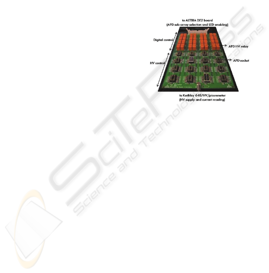
3.1 APD Tester
The APD Tester is a dedicated electronic setup for
the Hamamatsu APD array S8550 gain and dark
Current quality control and characterization (Figure
5). One of the main features of this dedicated
electronic system is the automatization of the
measurement procedure, in order to save time and
manpower. It measures 16 APD arrays (32 sub-
arrays) in a single run (or several), in about 4 hours.
It also controls the blue LED, used to simulate the
scintillation light.
Figure 5: APD Tester, an electronic setup designed to the
automatic characterization of the S8550 APD Array.
The electronic was completely designed and
developed at LIP. The Tester was assembled inside a
metal box (Faraday cage) due to the need of a
protection from any outside signal interference, and
to keep the APD arrays away from the outside light.
The LED is located inside the box and is coupled to
a light guide to provide an equal light distribution to
all APD sub-arrays (and pixels). The tester setup is
composed by two major parts: HV Control and
Digital Control.
The digital control is composed by HV relays to
select the APD sub-array to be measured, from the
possible 32. The relays are controlled through a
FPGA Cyclone II (ALTERA DE2 Board) via serial
port. The LED is also controlled by the digital part.
The HV Control receives the HV from a Keithley
6487 Picommeter/Voltage Source, controlled via
serial port, and delivers it to the enabled APD sub-
array. The automatic setup, and the Keithley, are
controlled via serial ports by a LabView program,
which selects the measurement type and collects the
data into an excel file.
AVALANCHE PHOTODIODES FOR HIGH-RESOLUTION PET IMAGING SYSTEMS
35
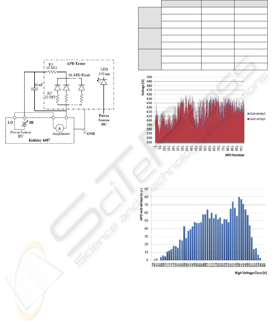
3.2 Experimental Setup
The experimental setup is composed by the APD
Tester (in the Faraday cage), a Keithley 6487
Picoammeter / Voltage Source and a PC. The gain
calculation assumes that when the APD sub-array is
biased at 30V (with the LED on), the gain is 1. From
that value the M=70, 150 and 350 are calculated. For
the dark current measurements the LED is turned off
and the residual current is measured. The schematic
of the experimental setup can be found in Figure 6.
Figure 6: Schematic representation of the experimental
setup for gain and dark current measurements.
3.3 Measurement Procedure
Each measurement run is accompanied by a stability
check procedure (performance on a reference APD
array) in order to evaluate the setup in terms of
significant variations on the studied parameters. The
setup operates at a stable temperature (through AC
control) of approximately 24ºC, in order to minimize
temperature dependence deviations. The complete
measurement took about 30 working days (2 run sets
per day approximately). The stability check consists
in the measurement of a predefined APD array, the
control APD. Each measurement run characterized
15 new APD plus the control APD.
3.3.1 Bias Voltage Quality Control and
Characterization
The 984 APD matrices (1968 sub-arrays) were
characterized in bias voltage terms and Table 2
summarizes the results.
All APD passed the HV QC at M=70 (the bias
voltage values were all below 500V) -
Figure
7. The HV values oscillated between 360
and 459 V - Figure 8.
Table 2: Bias Voltage average values for gains M=70, 150
and 350 from the 984 APD arrays (also the maximum and
minimum HV).
Bias Voltage (V) Sub-array 1 Sub-array 2
M=70
Average (r.m.s) 419 ± 22 418 ± 21
Minimum 360 364
Maximum 458 459
M=150
Average (r.m.s) 434 ± 22 434 ± 21
Minimum 375 379
Maximum 473 474
M=350
Average (r.m.s) 443 ± 22 442 ± 21
Minimum 384 389
Maximum 482 481
Figure 7: High Voltage per APD sub-array distribution at
M=70.
Figure 8: High Voltage histogram for M=70 values.
3.3.2 Gain Variation Quality Control and
Characterization
The gain variation of the 984 APD matrices was
characterized and Table 3 summarizes the results.
All but one APD sub-array had a gain variation
of less than 4%/V, passing the Gain variation quality
control at M=70 – Figure 9.
BIODEVICES 2009 - International Conference on Biomedical Electronics and Devices
36
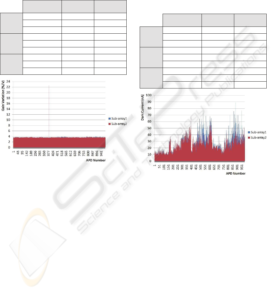
The APD that didn’t pass the QC procedure had
a dM/dV of about 22.7 % on the second sub-array
(the other had a normal value, 3.2 %/V).
Table 3: Gain Variation average values for gains M=70,
150 and 350 from the 984 APD arrays (also the maximum
and minimum dM/dV).
Gain Variation
(%/V)
Sub-array 1 Sub-array 2
M=70
Average (r.m.s) 3.6 ± 0.1 3.6 ± 0.6
Minimum 3.2 3.3
Maximum 4.0 22.7
M=150
Average (r.m.s) 6.3 ± 1.8 6.0 ± 0.8
Minimum 5.4 5.4
Maximum 26.5 19.4
M=350
Average (r.m.s) 14.0 ± 4.7 13.5 ± 4.6
Minimum 9.2 6.0
Maximum 30.7 31.6
Figure 9: Gain Variation per APD sub-array distribution at
M=70.
3.3.3 Dark Current Quality Control and
Characterization
The Dark Current characterization of the 984 APD
matrices was completed and
Table 4 summarizes the
results.
All APD sub-array passed the Dark Current QC
at M=70 (all the values were below the stipulated
maximum limit of 160nA, less than 10 nA per APD
pixel according to Hamamatsu Photonics) – Figure
10.
4 CONCLUSIONS
The quality control and characterization procedure
for the acquired APD arrays for the Clear-PEM
prototype was defined and implemented. A
dedicated automatic APD characterization
electronics was developed and built. The 984
Hamamatsu S8550 APD arrays were submitted to
the QC and characterization procedure at gains 70,
150 and 350, in terms of bias voltage, dark current
and gain variation per volt.
Table 4: Dark Current average values for gains M=70, 150
and 350 from the 984 APD arrays (also the maximum and
minimum Id).
Dark Current
(nA)
Sub-array 1 Sub-array 2
M=70
Average (r.m.s) 27.1 ± 13.3 24.2 ± 10.1
Minimum 7.8 8.2
Maximum 88.9 67.6
M=150
Average (r.m.s) 43.1 ± 21.1 40.0 ± 19.2
Minimum 10.1 12.1
Maximum 138.4 300.0
M=350
Average (r.m.s) 107.1 ± 67.0 103.7 ± 65.9
Minimum 15.9 17.6
Maximum 334.2 700.0
Figure 10: Dark Current per APD sub-array distribution at
M=70.
The QC (M=70) had very good results: average
bias voltage of 419 and 418V for sub-array1 and 2
respectively, average dark current of 27.1 and
24.2nA, for sub-array1 and 2, and average gain
variation of 3.6%/V for both sub-arrays.
From a total of 984 tested APD arrays only 1
(0.1%) didn’t pass the QC procedure (due to a
22.7%/V gain variation in the second sub-array).
The small variance on the different electrical
characterization parameters points out that current
available APDs are suitable for high-integration PET
prototypes which could not be implemented using a
classical photomultiplier readout.
AVALANCHE PHOTODIODES FOR HIGH-RESOLUTION PET IMAGING SYSTEMS
37

ACKNOWLEDGEMENTS
The authors would like to thank colleagues from the
Portuguese PET Consortium and the Crystal Clear
Collaboration for their suggestions and contribution.
This project is financed by AdI (Agência de
Inovação) and POSI (Operational Program for
Information Society), Portugal. The work of P.
Rodrigues and A. Trindade was supported by FCT
under grants SFRH/BPD/37233/2007 and
SFRH/BPD/37226/2007. The work of R. Bugalho,
B. Carriço, C. S. Ferreira, R. Moura, C. Ortigão and
J. F. Pinheiro was supported by AdI.
REFERENCES
Abreu, M. C., Aguiar, J. D., Almeida, F. G., Almeida, P.,
Bento, P., Carriço, B., Ferreira, M., Ferreira, N. C.,
Gonçalves, F., Leong, C., Lopes, F., Lousã, P.,
Martins, M. V., Matela, N., Mendes, P. R., Moura, R.,
Nobre, J., Oliveira, N., Ortigão, C., Peralta, L.,
Pereira, R., Rego, J., Ribeiro, R., Rodrigues, P.,
Sampaio, J., Santos, A. I., Silva, L., Silva, J. C., Sousa,
P., Teixeira, I. C., Teixeira, J. P., Trindade, A.,and
Varela, J. (2006). Design and evaluation of the Clear-
PEM scanner for positron emission mammography.
IEEE Trans. Nuc. Sci., 53:71–77.
Abreu, M. C., Amaral, P., Carriço, B., Ferreira, M.,
Moura, R., Ortigãoo, C., Rato, P., and Varela, J.
(2007). Characterization and quality control of
avalanche PhotoDiode arrays for the Clear–PEM
detector modules. Nucl. Instr. and Method.,
576(1):19–22.
Albuquerque, A., V. Bexiga, Bugalho, R., Carriço, B.,
Ferreira, C. S., Ferreira, M., Godinho, J. Gonçalves,
F., Leong, C., Lousã, P., Machado, P., Moura, R.,
Neves, P., Ortigão, C., Piedade, F., Pinheiro, J. F,
Rivetti, A., Rodrigues, P., Silva, J. C., Silva, M. M.,
Teixeira, I. C., Teixeira, J. P., Trindade, A., Varela, J.
(2008) Experimental characterization of the 192
channel Clear–PEM frontend ASIC for multi–pixel
APD readout. Sub. Nucl. Instr. And Method.
Albuquerque, E., Almeida, F. G., Almeida, P., Augusto,
S., Bexiga, V., Bugalho, R. Carmona, S. , Carriço, B.,
Ferreira, C. S., Ferreira, N. C., Ferreira, M., Godinho,
J., Gonçalves, F., Guerreiro, C., Leong, C., Lousã, P.,
Machado, P., Martins, M. V., Matela, N., Moura, R.,
Neves, P., Oliveira, N., Ortigão, C., Piedade, F.,
Pinheiro, J. F., Rego, J., Relvas, P., Rivetti, A.,
Rodrigues, P., Sá, D. N., Sampaio, J., Santos, A. I.,
Silva, M. M., Teixeira, I. C., Teixeira, J. P., Silva, J.
C., Trindade, A., Varela, J. Performance evaluation of
a highly integrated APD/ASIC double-readout
supermodule with 768 channels for Clear-PEM, In
2008 IEEE Nuclear Science Symposium Conference
Record.
Amaral, P., Carriço, B., Ferreira, M., Moura, R., Ortigão,
C., Rodrigues, P., Silva, J. C., Trindade, A., and
Varela, J. (2006). Performance and quality control of
Clear–PEM detector modules. Nucl. Instr. and
Method. in press.
Albuquerque, E., Bento, P., Leong, C., Gonçalves, F.,
Nobre, J., Rego, J., Relvas, P., Lousã, P., Rodrigues,
P., Teixeira, I. C., Teixeira, J. P., Silva, L., Silva, M.
M., Trindade, A., and Varela, J. (2006). The Clear-
PEM electronics system. IEEE Trans. Nuc. Sci.,
53(5):2704–2711.
Crespo, P., Kapusta, M., Pawelke, J., Moszyński, M., and
Enghardt, W. (2004). First in–beam PET imaging with
LSO/APD array detectors. IEEE Trans. Nuc. Sci.,
51(5):2654–2661.
Kapusta, M., Crespo, P., Wolski, D., Moszyński, M., and
Enghardt, W. (2003). Hamamatsu S8550 arrays for
high–resolution scintillator matrices readout. Nucl.
Instr. and Method., A504:139–142.
P. Lecoq and J. Varela, Clear-PEM, a dedicated PET
camera for mammography. Nucl. Instrum. Meth. vol
A 486, pp.1-6, 2002.
Melcher, C. L. and Schweitzer, J. S. (1992). Cerium–
doped lutetium oxyorthosilicate: a fast, efficient new
scintillator. IEEE Trans. Nuc. Sci., 39(4):502–505.
Moses, W. W. (2004). Positron emission mammography
imaging. Nucl. Instr. and Method., A525(1–2).
Mosset, J. B. (2006). Developpement d’un module de
d´etection phoswich LSO%LuYAP pour le prototype
de camera `a positrons ClearPET. PhD thesis, Faculte
des Sciences de base de l´Ecole Polytechnique
Federale de Lausanne.
Rodrigues, P.,. (2007). Study and Development of the
Clear-PEM Trigger and Data Acquisition System
ClearPET. PhD thesis, Instituto Superior Técnico,
Universidade Técnica de Lisboa.
Spanoudaki, V., McElroy, D. P., Zell, K., and Ziegler, S. I.
(2005). Effect of temperature on the stability and
performance of an LSO–APD PET scanner. In 2005
IEEE Nuclear Science Symposium Conference
Record, pages 2785–2789.
Shao, Y., Silverman, R. W., Farrell, R., Cirignamo, L.,
Grazioso, R., Shah, K. S., Visser, G., Clajus, M.,
T¨umer, T. O., and Cherry, S. R. (2000). Design
studies of a high resolution PET detector using APD
arrays. IEEE Trans. Nuc. Sci., 47(3):1051–1057.
Thompson, C. J. , Murthy, K., Picard, Y. , Weinberg, I. N.
, Mako F. M. (1995) Positron Emission
Mammography (PEM): a promising technique to
detect breast cancer. IEEE Trans. Nucl. Sci. 42 1012–
1017.
BIODEVICES 2009 - International Conference on Biomedical Electronics and Devices
38
