ON-DETECTOR ELECTRONICS
OF THE CLEAR PEM SCANNER
E. Albuquerque
1
, V. Bexiga
1
, R. Bugalho
2
, B. Carriço
2
, C. S. Ferreira
2
, M. Ferreira
2
, J. Godinho
3
F. Gonçalves
1
, C. Leong
1
, P. Lousã
3
, P. Machado
1
, R. Moura
2
, P. Neves
3
, C. Ortigão
2
, F. Piedade
3
J. F. Pinheiro
2
, P. Relvas
3
, A. Rivetti
4
, P. Rodrigues
2
, J. C. Silva
2,6
, M. M. Silva
1
, I. C. Teixeira
1,5
J. P. Teixeira
1,5
, A. Trindade
2
and J. Varela
2,5,6
1
INESC-ID - Inst. de Engª de Sistemas e Computação, Investigação e Desenvolvimento, Lisboa, Portugal
2
LIP - Lab. de Instrumentação e Física Experimental de Partículas, Lisboa, Portugal
3
INOV – Inst. de Novas Tecnologias, Lisboa, Portugal
4
INFN - Istituto Nazionale di Fisica Nucleare, Torino, Italia
5
also with Inst. Superior Técnico, Univ. Técnica de Lisboa, Portugal
6
also with CERN, Geneva, Switzerland
Keywords: PET, Scanner, Breast, Cancer, SPECT.
Abstract: A Portuguese consortium has developed a PET scanner dedicated to breast cancer detection (Clear-PEM
scanner) within the framework of the international Crystal Clear Collaboration at CERN. In the construction
of this scanner several challenges have been addressed, from the design of the photon’s detector, front-end
electronics and data acquisition systems up to the image reconstruction algorithms. In this paper we describe
the development of the electronics in the detector heads needed to read-out and filter the data from 12288
detector channels, as well as to provide regulated high-voltages, low voltage power and control signals, and
also to monitor the environment in the detector heads. The scanner is currently in its final phase of
integration and will soon be installed in the department of Nuclear Medicine of Hospital Garcia de Orta and
Instituto Português de Oncologia (Porto) were clinical trials will be conducted.
1 INTRODUCTION
The Clear-PEM detector is a Positron Emission
Mammography scanner that was developed by
several Portuguese institutions within the framework
of the international Crystal Clear Collaboration at
CERN (
Abreu, 2006).
The detector assembly is based on two detecting
planar heads. The detection heads are mounted on a
robotized mechanical system, enabling the exam of
both breasts, one at a time, as well as the axillary
lymph nodes.
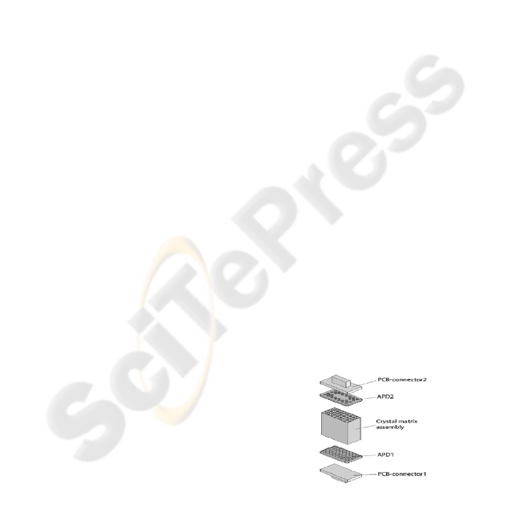
The basic element of the scanner is the detector
module (Fig. 1). Each module has 32 LYSO:Ce
crystals with 2x2x20 mm
3
assembled in a matrix
coupled on both ends to avalanche photo-diodes
(APD) (Amaral, 2007). Twelve of these detector
modules are assembled in a mechanical structure
placed between two Frontend boards forming a
Supermodule (Fig. 2).
355
Albuquerque E., Bexiga V., Bugalho R., Carric¸o B., Ferreira C., Ferreira M., Godinho J., Gonc¸alves F., Leong C., Lous
˜
a P., Machado P., Moura R., Neves
P., Ortig
˜
ao C., Piedade F., Pinheiro J., Relvas P., Rivetti A., Rodrigues P., Silva J., Silva M., Teixeira I., Teixeira J., Trindade A. and Varela J. (2009).
ON-DETECTOR ELECTRONICS OF THE CLEAR PEM SCANNER .
In Proceedings of the International Conference on Biomedical Electronics and Devices, pages 355-358
Copyright
c
SciTePress
The traditional readout based on photomultipliers
is replaced by multi-pixel APDs. Due to its
compactness, it is possible to read each single crystal
with one APD pixel on each end, and to use the
relative amplitude of the two signals to estimate the
longitudinal coordinate of the photon interaction.
The individual 1:1 crystal-APD pixel coupling
leads to 12 288 detector channels, with a density at
about 13 channels per centimeter square. The limited
available space in the detector heads demand that all
the processing electronics must have a strict limited
power consumption budget. This and the low gain
(100) of the APDs, has lead to the development, for
the Clear-PEM scanner, of specifically tailored low-
noise Application-Specific Integrated Circuit (ASIC).
Frontend electronics boards based on the Clear-
PEM ASICs provide the first level of signal
processing, including readout, amplification,
sampling and storage in analogue memories of the
APD array signals.
The ASIC’s output pulses are digitized by free-
sampling ADCs in the Frontend boards. LVDS data
links are used to transmit the detector data to the off-
detector electronics system, which implements the
first-level trigger, and data concentration and
transmission to the data acquisition server
(Albuquerque, 2008).
Auxiliary service boards located in the detector
heads are needed to provide regulated high-voltages
for each of the APD arrays and to distribute low
voltage power as well as control and clock signals.
The electronics is also responsible to monitor the
detector heads environment (temperature and
pressure).
Each Clear-PEM detector head has a total 3072
crystals grouped in 96 detector modules and 8
Supermodules. The detector head includes also one
Service Board, one high-voltage connection Matrix
Board and one clock fan-out unit. These electronics
boards are described in the following sections.
2 THE FRONT END
ELECTRONICS SYSTEM
The Frontend electronics system is one of the most
challenging and innovative sub-systems of the
Clear-PEM detector. It is composed by the Frontend
boards which interface directly with the APD arrays
assembled in the detector modules and are connected
to the Auxiliary Boards in the detector head.
The system, physically located on the detector
heads, performs signal amplification, channel
selection and analog multiplexing, analog to digital
conversion and parallel-to-serial translation.
A frontend ASIC has been developed for readout
of the multi-pixel S8550 Hamamatsu APDs.
Themixed-signal ASIC incorporates 192 low-noise
charge pre-amplifiers, shapers, analogue memory
cells and digital control blocks. Pulses are
continuously stored in memory cells at clock
frequency. Channels above a common threshold
voltage are readout for digitization by off-chip free
sampling ADCs. The number of output channels of
the frontend ASIC is two, still allowing for the
readout of two-hit Compton interactions in the
detector. The ASIC has a size of 7.3 mm x 9.8 mm
and was designed in 0.35 µm CMOS technology.
The Frontend Board (FEB) integrates two 192
channels ASICs and two dual free-sampling 10-bit
ADC chips working at frequencies up to 100 MHz.
The digitized data is transmitted to the off-detector
data acquisition system by LVDS serial links at 600
MHz.
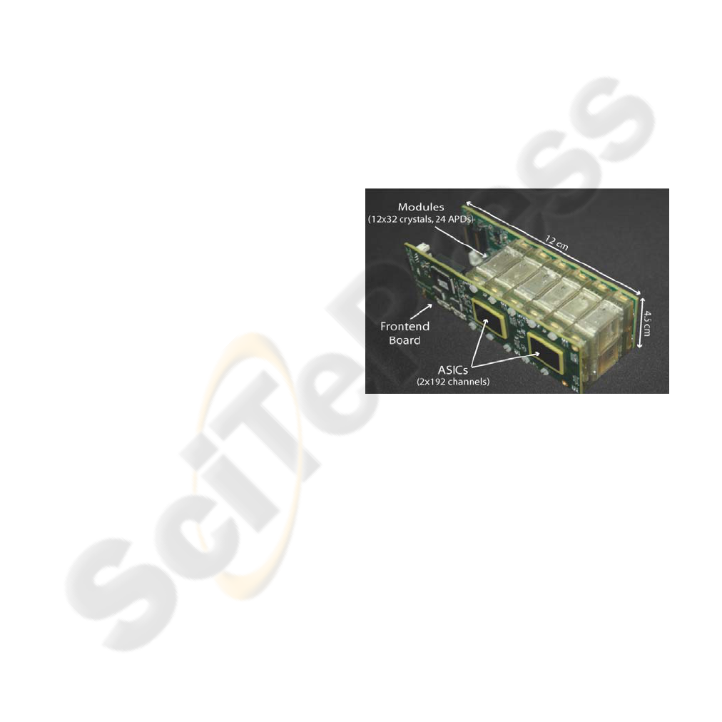
Figure 2: Supermodule structure assembling 12 modules,
each with 32 LYSO:Ce crystals and two 32-pixel APD
arrays in double readout. Each Frontend board has two
ASICs with 192 input channels.
Two FEBs are used to mount one supermodule
structure with a total of 768 electronic channels and
dimensions of 12x4.5 cm
2
as illustrated in Fig. 2.
The frontend electronics must have low-noise
due to the initial reduced charge at the amplifier
input, which for a 511 keV photon energy deposit is
around 30fC (maximum value). The frontend ASIC
amplifies this charge by about three orders of
magnitude, while complying with the low-power
dissipation requirements (5 mW/channel),
compatible with a compact water based cooling
system that allows to operate the detector at 18
o
C. A
temperature stability of the order of 0.1
o
C
is
required since the LYSO:Ce light yield and APD
BIODEVICES 2009 - International Conference on Biomedical Electronics and Devices
356
gain are inversely dependent on the temperature (2-
3%/
o
C).
The Frontend Boards have a mixed analog-digital
environment and therefore special care is needed
regarding the correct conditioning of the digital,
large amplitude, high-frequency clock and other
periodic signals. Noise pickup in the PCB traces that
connect the APD outputs to the frontend chips must
also be minimized.
The performance of the Supermodules was
evaluated in a setup that integrates all the electronics
and data acquisition sub-systems as it will operate in
the final detector. A cooling system based on
controlled flux of cold water was build to cope with
the power dissipation from the Frontend Boards
during the qualification tests.
Acquisition runs with
22
Na and
137
Cs radioactive
sources, as well as background acquisitions from the
176
Lu natural radioactivity of the LYSO:Ce crystals
have been performed
(R. Bugalho, 2008).
The energy and time resolutions, energy linearity
of detector readout chain and output channels
occupancy are the parameters under evaluation for
each supermodule.
The noise of the detector channels, defined as the
equivalent noise charge (ENC) at the amplifier
inputs, is around 1300 e
-
RMS. This noise
contributes less than 2% to the energy resolution,
which at 511 keV is dominated by the fluctuations of
the scintillating light signal in the crystals. This
noise level implies a RMS time resolution of
individual 511 keV photons of the order of 1 ns.
3 THE AUXILIARY BOARDS
Several auxiliary boards have been designed to
provide regulated high-voltages, low voltage power,
as well as clock and control signals to the
Supermodules, and also to monitor the temperature
and pressure inside the detector heads.
These boards are placed in the back side of the
detector head, leaving the front side free of obstacles
for the detection of the PET photons.
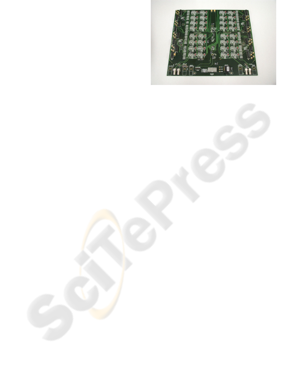
The main auxiliary board is the Service Board
(SB) shown in figure 3.
Dedicated circuits in the SB including remotely
controlled Digital to Analog Converters (DAC) are
used to regulate the high-voltage (HV) lines (350-
500V) needed for the polarization of the APDs.
Plugging directly on the SB, the HV Matrix is
another auxiliary board that provides the
connections of the HV lines to the APD arrays
(figure 4).
Figure 3: View of the Service Board.
The connection matrix distributes 32 different
high-voltage references to the 384 APDs sub-arrays
(16 pixels) in the detector head. The APD gain
variation is of the order of 6%/V which requires a
stability of the biasing voltages better that 0.1 V.
The ripple of the high-voltage lines is less than 0.02
V. Before assembly each HV channel is calibrated in
order to guarantee that the gain of the APDs is
100.External power supplies provide independent
low-voltages for the analog and digital sections of
the detector electronics. The SB organizes the
distribution of these voltages to the Frontend Boards.
The control of the ASICs reset sequence uses an
Altera FPGA in the Service Board, and the setting of
the voltage thresholds of signal detection in the
ASICs is done by DACs controlled remotely via I2C.
The measurement of the temperature in the
detector modules uses PT100 sensors placed in
contact with the APD arrays, coupled to dedicated
signal conditioning circuits followed by ADCs
accessed remotely by the I2C control lines. The
pressure inside the detector head is also measured to
assure that slightly over-pressured nitrogen fills the
detector heads avoiding water condensation.
The system clock and a synchronization signal
are distributed to the frontend electronics. To avoid
interferences of the clock with the high-voltage lines,
a dedicated board is used to fan-out the clock and
sync signals.
Finally the detector head are closed using a
specifically designed patch panel board equipped
with vacuum tight connectors to insure the detector
box hermeticity (fig 4).
ON-DETECTOR ELECTRONICS OF THE CLEAR PEM SCANNER
357
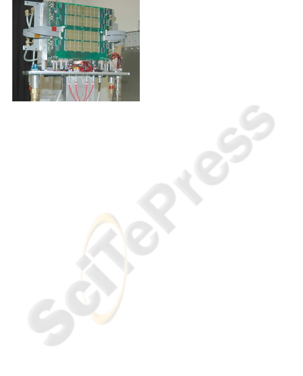
Figure 4: View of a detector head, with the hermetic patch
panel on bottom, during the cabling phase.
4 CONCLUSIONS
In this paper, the detector electronics of the Clear-
PEM scanner, composed of the Frontend Boards
connecting directly with the detector modules and of
the Auxiliary Boards in the detector heads, was
presented. The detector electronics system is one of
the most challenging and innovative sub-systems of
the Clear-PEM scanner.
This electronics was validated in an experimental
setup that includes detector supermodules and all the
external sub-systems developed for the Clear-PEM
scanner, including the data acquisition electronics
and computing systems. The measured electronic
noise levels in the detector are below the
requirements set by the Clear-PEM specifications.
REFERENCES
Abreu et al. “Design and Evaluation of the ClearPEM
Scanner for Positron Emission Mammography”,
IEEE Trans. Nucl. Sci. (2006), Vol.53(1), pp 71-7.
Amaral et al. “Performance and quality control of Clear–
PEM detector modules”, Nucl. Instrum. And Meth. In
Phys. Res. (2007) A580, 1123-1126.
R. Bugalho et al. “Validation of Clear-PEM Data
Acquisition Electronics and Operation Software” sub.
IEEE NSS-MIC 2008.
Albuquerque et al. “Performance Evaluation of a Highly
Integrated APD/ASIC Double-Readout Supermodule
with 768 Channels for Clear-PEM” sub. IEEE NSS-
MIC 2008.
BIODEVICES 2009 - International Conference on Biomedical Electronics and Devices
358
