HARDWARE IMPLEMENTATION FOR EDGE
DETECTION IN CDNA MICROARRAY IMAGES
Bogdan Belean, Monica Borda
Technical University of Cluj-Napoca, Faculty of Electronics Teleomunications and Information Technology
Comunications Department, 26 28 George Baritiu, Cluj-Napoca, Romania
Albert Fazakas
Technical University of Cluj-Napoca, Faculty of Electronics Teleomunications and Information Technology
Electronics Basics Department, 26 28 George Baritiu, Cluj-Napoca, Romania
Keywords: cDNA Microarray, Image Processing, Parallel Processing, FPGA Technology.
Abstract: The present paper proposes hardware implementation strategies for cDNA microarray image processing in
order to overcome the main disadvantage introduced by the existing computational tools, the increased
processing time. A hardware implementation of the Canny edge detection algorithm for microarray spots is
described. The implementation takes advantage of spatial and temporal parallelism offered by FPGA
technology. Results of the hardware implementation which prove time and cost efficiency are presented.
1 INTRODUCTION
Microarray experiments are providing genome wide-
data on gene expression patterns. Different
techniques including SAGE, differential display,
oligonucleotide array and cDNA microarrays have
been developed. The techniques offer the possibility
of mRNA expression to be assessed on a global
scale, allowing the parallel assessment of gene
expression for thousands of genes in a single
experiment. Gene expression represents the
transformation of gene’s information into proteins.
The most common use of these techniques is for the
determination of patterns of differential gene
expression, comparing differences in mRNA
expression levels between identical cells subjected
to different stimuli or between different cellular
phenotypes or developement stages (Bajcsy, 2004).
The hardware processing techniques described in
this paper will focus on processing images obtained
as a result of cDNA microarray experiment. cDNA
microarrays represent gene specific probes arrayed
on a matrix such as a glass slide or microchip.
Usually, samples from two sources are labelled with
two different fluorescent markers and hybridized on
the same array (glass slide). After the hybridization,
the array is scanned using two light sources with
different lengths (red and green) to determine the
amount of labelled sample bound to each spot
through hybridization process. The light sources
induce fluorescence in the spots, which is captured
by a scanner and a composite image is produced.
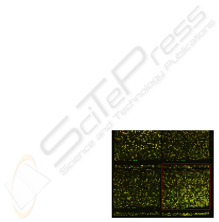
Figure 1: Microarray image with underlined independent
sub-image. Stanford University Medical Centre,
Department of Genetics.
359
Belean B., Borda M. and Fazakas A. (2009).
HARDWARE IMPLEMENTATION FOR EDGE DETECTION IN CDNA MICROARRAY IMAGES .
In Proceedings of the International Conference on Biomedical Electronics and Devices, pages 359-363
DOI: 10.5220/0001536403590363
Copyright
c
SciTePress

Further on, image processing techniques are used
to quantify gene expression levels present in the
captured microarray image, in order to identify a
gene in a biological sequence and to predict the
function of the identified gene. The flow of
processing a microarray image (Yang, 2001) is
generally separated in the following tasks:
addressing, segmentation, intensity extraction and
pre-processing to improve image quality and
enhance weakly expressed spots. The first step
associates an address to each spot of the image. In
the second one, pixels are classified either as
foreground, representing the cDNA spots, or as
background. The last step calculates spot intensities
and estimates background intensity values.
The major tasks of microarray image processing,
which contributes in fulfilling the last mentioned
steps, are to identify the array format including the
array layout, spot size and shape, spot intensities and
distances between spots. The main parameters taken
into consideration in microarray image processing
are accuracy and time. The accuracy is given by the
quality of image processing techniques. The second
parameter, time, is critical due to the large amount of
data contained in a microarray image. A regular
microarray image has up to hundreds of MB, and it
can be divided in independent sub-images, which
consists in a compact group of spots as it can be seen
in figure 1. Sophisticated computational tools are
available for microarray image processing but, their
main disadvantages are the increased computational
time and the user intervention needed in processing.
To overcome the previous disadvantages,
microarray images are analyzed and processed using
FPGA technology. The hardware implementations
of microarray image processing techniques make use
of the features of FPGA, which allow accessing at
the same time hundreds of memory addresses. In this
way, calculations specific to microarray image
processing are made in parallel, increasing the
processing speed. For this kind of processing, image
acquisition is mandatory and its description is
presented in the following papers (Belean, 2008).
This paper proposes hardware strategies for
microarray image processing (paragraph 2), and also
an implementation of spot border detection
algorithm using the Canny filter.
2 FPGA & MICROARRAYS
FPGA technology uses pre-built logic blocks and
programmable routing resources to configure these
chips and to implement custom hardware
functionality. Their main benefits are the low cost,
the short time to market and also the increased
performance due to their structure which is able to
exploit spatial and temporal parallelism. These
advantages will be used to develop a system on a
chip in order to process the microarray images in a
manner that does not need user intervention. Also,
time being critical in microarray image processing,
using FPGA technology will decrease the
computational time due to its parallel computation
capabilities. The main goal of this approach for
microarray image processing is to obtain a device
which will be able to extract and quantify gene
expression a lot more faster than existing
computational tools, so that microarray analyses to
be easily performed on a large number of subjects
(thousands of patients and different diseases). This
task can hardly be achieved with the existing tools
which are time consuming and which also need user
intervention.
2.1 Hardware Implementation for
Microarray Image Processing
The hardware implementation strategies for
microarray image processing techniques presented in
this paper takes advantage of the structure size and
shape of a microarray image. As in figure 1, a piece
of the microarray image is delimited, and represents
an independent microarray sub-image. Taking into
account that the microarray image composed by
independent sub-images is written in a RAM
memory after the acquisition, a first step in
processing is to crop the image by determining the
address and dimension of each sub-image. Once
these parameters are known, the independent sub-
images are copied one by one in the Block RAM
memory inside the FPGA for further processing
which consists in addressing each spot of the image.
This type of memory offers multi-port and high
speed access needed for the next step of processing
which aims to determine the spot contour and extract
the spot intensity for quantifying gene expression.
The image being cropped and copied into the
Block RAM memory, hardware design techniques
such as parallelism and pipelining can be developed
using FPGA technology. These techniques will be
presented in the next subchapters.
2.1.1 Hardware Algorithms
Image processing operations like median filters and
gradient calculation are based on the convolution,
which is included in a class of algorithms called
BIODEVICES 2009 - International Conference on Biomedical Electronics and Devices
360
spatial filters. Convolution is used for implementing
image operators which have as output pixel value a
linear combination between pixels of the original
image. Conceptually, each pixel in the output image
is produced by sliding an NxM window over the
input image and computing an operation according
to the input pixels under the window and the chosen
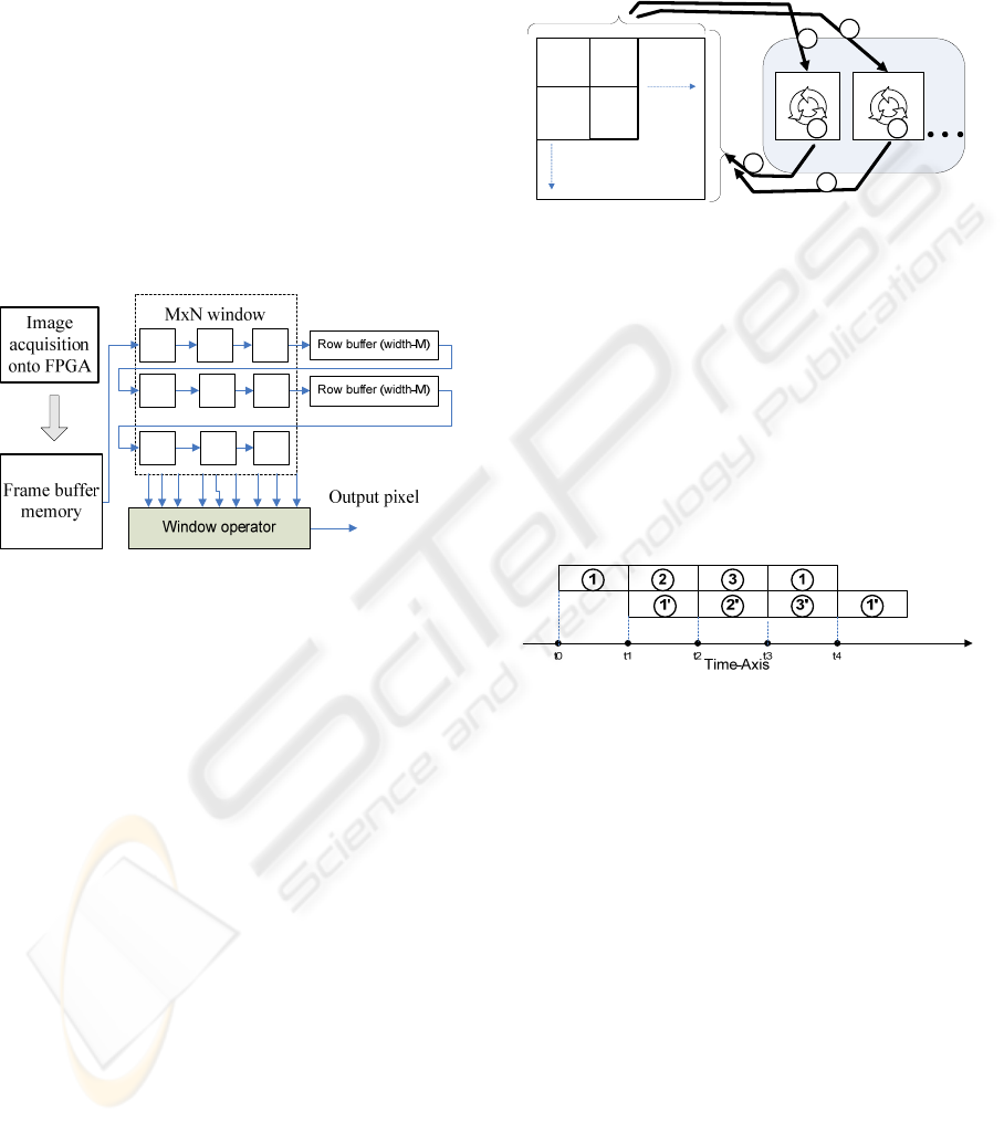
window operator. The hardware approach for
convolution is presented as follows: the entire input
image is stored into a frame buffer; each time the
window is moved, MxN pixels values are required to
calculate the resulted pixel value. Memory bandwith
constraints make obtaining all these pixels each
clock cycle impossible, so local caching is
performed. In this way, N-1 rows are cached using a
shift register which leads to the next block diagram:
Figure 2: Block diagram for hardware implementation of
convolution operator (Johnston, 2004).
In this case, instead of sliding a window across
the image, the implementation feeds the image
through the window.
2.1.2 Temporal Parallelism
Based on the possibility of cropping a microarray
image into independent sub-images, a strategy for
microarray image processing emerges. The idea is to
design an architecture which processes in parallel
two or more independent sub-images. Once the
address and dimension of each independent sub-
image is determined, two ore more microarray sub-
images can be copied into the FPGA block RAM
depending on the capacity of block RAM. In figure
3 a cropped microarray image which consists in a
matrix of independent sub-images called A(i,j) is
presented. The numbers from 1 to 3 and from 1’ to
3’ represent the operations applied on two
independent microarray sub-images. This way,
operation 1 stands for copying the sub-image from
RAM to the FPGA block RAM. Operation 2
represents the processing of the sub-image using
FPGA technology and spatial parallelism. Operation
3 copies the microarray processed sub-image back
into the RAM, on the exact place from which it was
transferred into FPGA. The operations 1, 2 and 3 are
done for each microarray sub-image. In the end we
will have in the RAM memory a processed
microarray image.
Figure 3: Block diagram for pipeline architecture of
microarray image processing.
Time beeing critical in microarray image
processing, the previous approach reduces the
processing time to half of its regular value. As an
exemple we can mention that, while a sub-image is
copied into the block RAM, image processing
techniques are applied on another independent sub-
image, in case that there is place for more than one
microarray independent sub-image in RAM. A view
in time of the current architecture can be seen in the
next figure:
Figure 4: Time representation of the operation 1,2 and 3 in
pipelining.
2.1.3 Spatial Parallelism
To start with, it is to be mentioned that processors
divide computation across time, while dedicated
logic divides it across space, which highly decreases
computational time. Taking into consideration the
large amount of data contained in a microarray
image and also the repetitive nature of this type of
data, FPGA dedicated logic was chosen for the
implementation of microarray image processing
techniques in order to reduce computational time.
The use of hardware description language (HDL)
allows a description of a design with parallel data
paths and simultaneous computation.
Some of the major tasks in microarray image
processing are to extract spot intensities and to
determine spot contour and dimension. The
dimension of a regular spot is around 20-40 pixels
height and length. The reduced dimension of a
A(0,0) A(0,1)
A(1,0) A(1,1)
FPGA
Block RAM
A(i,j)
A(i,j)+1
Cropped microarray image
representation
in RAM memory
1
2
3
1'
2'
3'
HARDWARE IMPLEMENTATION FOR EDGE DETECTION IN CDNA MICROARRAY IMAGES
361
microarray spot offers the possibility to exploit
spatial parallelism capabilities of FPGAs. Each spot
is copied into the distributed RAM of the FPGA, so
spatial computation can be applied, thanks to the
simultaneous access to each pixel.
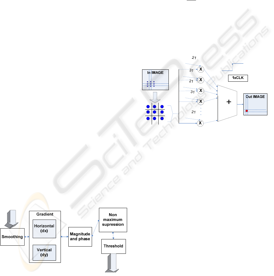
3 HARDWARE
IMPLEMENTATION
This paper presents a hardware implementation of an
adaptive edge detection filter using FPGA, which
provides the necessary performance for fast
microarray image processing. In microarray image
processing, edge detection is a fundamental tool
used as a precursor step to intensity extraction and
spot segmentation. Edges occur at images location
with strong intensity contrast. For edge detection a
high-pass filter in Fourier domain can be applied, or
convolution with an appropriate kernel (Sobel,
Prewitt etc.) in the spatial domain is useful.
Convolution in the spatial domain has been chosen
for implementation because it is computationally
less expansive and offers better results.
The algorithm used for the hardware
implementation is Canny algorithm, which is
considered to be optimal, based on the following: it
finds the most edges, marks the edge as close as
possible to the actual edges, provides sharp and thin
edges. The filter that meets all the criteria mentioned
above can be efficiently approximated using the first
derivative of a Gaussian function. So the first two
steps in applying the Canny algorithm would be
smoothing the image and differentiating the image in
two orthogonal directions. The next step, non-
maximum suppression, computes the gradient
direction and magnitude in order to eliminate the
pixels that represent false edges.
Input
Output
Figure 5: Block diagram for Canny algorithm.
The previously described algorithm is applied on
a microarray spot. Due to its small dimension
(approximately 40x40 pixels), the whole spot is
copied into the FPGA, so hardware processing
strategies (spatial parallelism) described in the
previous paragraph can be applied. Further on, the
hardware implementations for each of the previous
steps are presented.
Smoothing operation is done using the following
convolution mask, because it contains a division by
2
8
that is easily done with an 8 bits shift operation:
213121
314831
213121
256
1
The effect of the previous Gaussian convolution is to
blur the image, eliminating noise. As it can be seen
in the next diagram, for processing 1 pixel only one
clock cycle is needed, because all the neighborhood
pixels used in computation are accessed at the same
time.
Figure 6: Gaussian filter implementation.
After smoothing the image, the next step is
gradient calculation in order to find the edge
strength of the spot. To determine the orthogonal
gradient at each pixel location, the following
convolution masks are used:
000
101
000
−
and
010
000
010 −
In this case, only arithmetic operations of addition
are used, so for the whole microarray spot written in
FPGA distributed RAM, a single clock cycle and
2x40x40 adders are enough to determine the resulted
image after applying the convolution masks.
The sign and value of the orthogonal components
of the gradient determined before are used in
estimating the magnitude and the direction of the
gradient. Once the direction of the gradient is
known, pixels values around the pixel being
analyzed are interpolated. The pixel that does not
represent a local maximum is eliminated, by
comparing it with its neighbors along the direction
of the gradient (non maximum suppression).
Combinational logic and basic operations of addition
BIODEVICES 2009 - International Conference on Biomedical Electronics and Devices
362
and shifting are used in implementation, so each
clock cycle one pixel it’s processed.
3.1 Experimental Results
The hardware platform used for implementation
includes the XC3S5000 and a quartz oscillator with
a frequency of 50 MHz used to generate the clock
signal. Summing up the time needed for each step of
the edge detection algorithm applied on a 20x20
pixels spot, a processing time of 3.2 μs is obtained.
This results leads to a processing rate of
approximately 250 Mbytes/second.
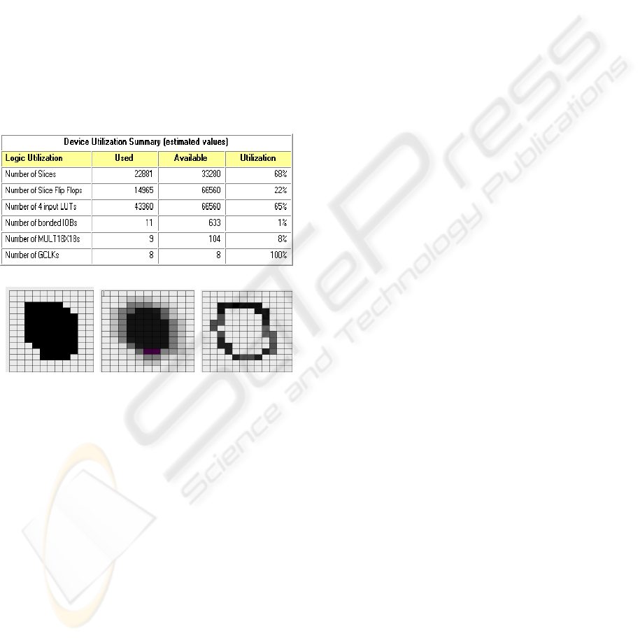
The next table presents the FPGA resource usage
for such an implementation.
Table 1: Statistics of FPGA (XC3S5000) resource usage
for edge detection of microarray spot.
(a) (b) (c)
Figure 7: Preliminary results obtained on a 20x20
microarray spot; a) original image, b) smoothed image,
c) edge detection.
The results of the implementation applied on a
microarray spot are presented in the previous figure.
4 CONCLUSIONS
The hardware implementation strategies for image
processing presented in this paper represent an
essential step for microarray image processing on a
hardware platform. The results of the hardware
implementation for edge detection in cDNA
microarray image emphasize the importance of
using hardware methods in cDNA microarray image
processing. The technology chosen to implement a
digital system for microarray image processing was
FPGA, due to its parallel computation capabilities
and to the possibility of reconfiguration.
To sum up, the experimental results made this
hardware technology a solution for realizing a fast,
cost efficient and accurate automated system for
cDNA microarray image processing.
ACKNOWLEDGEMENTS
This work was supported by PNII IDEI Nr.
332/2007 grant, code 909 and also by CNCSIS BD
scholarship.
REFERENCES
Bajcsy, P., 2004. An Overview of DNA Microarray Image
Requirements for Automated Processing, IEEE
Transactions on Image Processing, Vol. 13, No. 1, pp.
15-25
Yang, Y., Buckley, M., Dudoit, S., and Speed, T., 2001.
Comparison of methods for image analysis on cdna
microarray data, Department of statistics - University
of California – Berkeley, Technical Report 584
Li, Q., Fraley, C., Baumgarner,R., Yeung, K., and Raftery,
E., 2005. Donuts, scratches and blanks: Robust model-
based segmentation of microarray images,
Department of statistics - University of Washington.
Technical Report 473.
Belean, B., Borda, M., Fazakas, A., 2008, Adaptive
Microarray Image Acquisition System and Microarray
Image Processing Using FPGA Technolog. KES2008,
Springer (in print).
Johnston, C.T., 2004. Implementing image processing
algorithms on FPGA, Institute of Information Sciences
and Technology, Palmerston, New Zeeland
Blekas, K., Likas, A., Legaris, I., 2005. Mixture model
analysis of dna microarray images, IEEE Transactions
on medical imaging, pp. 901-909.
HARDWARE IMPLEMENTATION FOR EDGE DETECTION IN CDNA MICROARRAY IMAGES
363
