
AN ASYNCHRONOUS PROGRAMMABLE PARALLEL
2-D IMAGE FILTER CMOS IC BASED ON THE
GILBERT VECTOR MULTIPLIER
Rafał Długosz
Swiss Federal Institute of Technology in Lausanne, Institute of Microtechnology
Rue A.-L. Breguet 2, CH-2000, Neuchâtel, Switzerland
Vincent Gaudet
University of Alberta, Department of Electrical and Computer Engineering
ECERF Building, Edmonton Alberta, T6G 2V4, Canada
Keywords: Parallel and asynchronous 2-D analog filter, Gilbert vector multiplier, Ultra-low power dissipation.
Abstract: A novel analogue power-efficient 2-D programmable finite impulse response image filter is proposed. This
solution is based on the current-mode Gilbert-vector-multiplier operating in the weak inversion region,
which allows for ultra low power operation. The main advantage is in the asynchronous and parallel
calculation of all pixel values without using any clock generator. The filter is a programmable structure that
allows programmability of different filter masks both low-pass and high-pass. An experimental filter
integrated circuit with a resolution of 6x1 pixels dissipates in measurements a power of 30 μW at a data rate
of 30 kframes/s in a 180 nm CMOS technology. One of the intended applications of our proposed image
filter is in data compression in wireless endoscopic capsules.
1 INTRODUCTION
The advent of inexpensive CMOS image sensors has
recently led to the design of wireless capsules for
endoscopic diagnosis (Meng et al., 2004) (Xie et al.,
2006). Such capsules usually contain the CMOS
image sensor, signal processing circuitry, and a
communication block between the capsule and a
transceiver located outside the patient’s body that
records collected data. Such a system, together with
light-emitting diodes and a battery, is placed in a
small pill that is hermetically packaged to be robust
against enzymes and acid in the human digestive
tract. Such capsules must last 8 to 24 hours as they
travel throughout the digestive tract while capturing
about 50,000 photos that are then used for diagnostic
purposes. Thus the capsule must collect and transmit
an extremely large amount of information (Miaou,
2005). This problem is usually addressed by
different compression techniques e.g. a discrete
wavelet transform (DWT) (Miaou, 2005) and
recently reported near-lossless compression
algorithm for the images with a Bayer color filter
array (CFA) (Xie et al. 2006).
In these systems, analog data is typically
captured by a CMOS image sensor and then
processed in a specialized digital circuit (Xie et al.
2006). In this paper we propose a programmable
analog, asynchronous, parallel 2-D finite impulse
response (FIR) filter that can be used as a pre-
processing filter prior to the analog-to-digital
conversion (ADC) as well as in the filter banks in
the DWT-based compression algorithms. Our
proposed filter uses the current-mode Gilbert vector
multiplier circuit operating in the weak inversion
regime, leading to ultra-low power dissipation and
energy savings (Winstead, 2004), which is one of
main criterions in endoscopic capsule applications.
One of the advantages of this approach is the
speedup that results from the parallel and
asynchronous calculation of all pixel values without
using a clock generator.
Research has been conducted into analog image
filters for many years. An example image filter with
an array of 16x16 pixels that dissipates 165mW at
46
Długosz R. and Gaudet V. (2009).
AN ASYNCHRONOUS PROGRAMMABLE PARALLEL 2-D IMAGE FILTER CMOS IC BASED ON THE GILBERT VECTOR MULTIPLIER.
In Proceedings of the International Conference on Biomedical Electronics and Devices, pages 46-51
DOI: 10.5220/0001536800460051
Copyright
c
SciTePress
the I/O data rate of 5x10
7
events per second has been
described by (Serrano-Gotarredona et al., 2008).
This solution allows for connecting of many chips
into bigger systems with higher resolutions.
Image filters are also implemented using cellular
neural networks (CNN). An example filter of this
type, designed in a 0.5 μm CMOS technology, with
a resolution of 64x64 pixels at an I/O analog data
rate of 1 MSps, dissipates 1.5 W (Linan et al., 1999).
The experimental prototype filter described in
this paper has been designed for a resolution of 6x1
pixels, but as the circuit features a modular structure,
therefore it can be redesigned for higher resolutions.
Based on the simulation and the measurement
results, we project a power dissipation of 22 mW for
a 64x64 pixel filter operating at a throughput of 10
Mpixels/s (measurements) or even 4 Gpixels/s
(simulations) that means a significant improvement
in comparison to the solutions described above.
The paper is organized as follows. In next
section we present the circuits that we use for FIR
filtering. An experimental filter realized in TSMC
180nm CMOS process
is described in the subsequent
section together with selected measurement results.
Finally the last section concludes this paper.
2 GENERAL IDEA OF THE
PROPOSED IMAGE FILTER
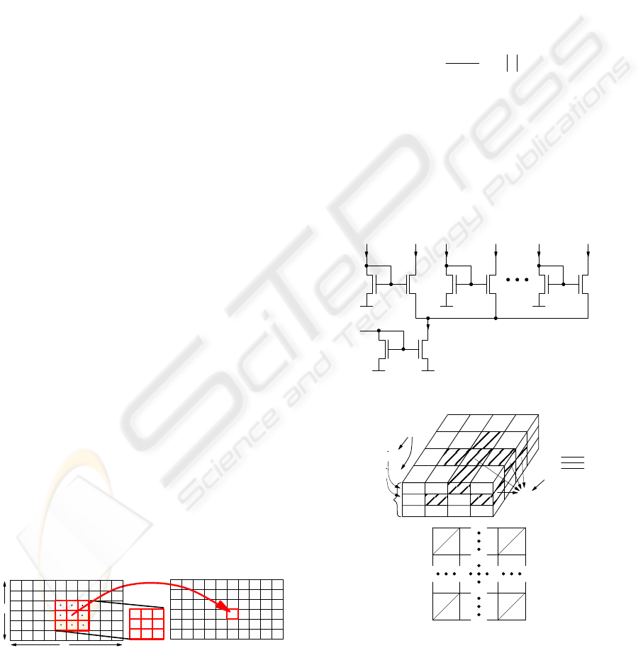
A basic 2-D FIR filtering scheme is shown in Fig. 1.
Pixels from a 2-D input signal A are first multiplied
by filter coefficients from a mask H. The products of
these operations are summed, thus producing pixels
for an output image B, according to the following
equation (for e.g. 3x3 mask H):
∑∑
==
−+−+=
3
1
3
1
),()2,2(),(
nm
mnhmynxAyxB
(1)
When the image filtering is implemented in DSP
systems the mask is moved over the input image A
and the output pixels are calculated sequentially,
which is a time and power consuming process.
Σ
A
- an input 2-D signal
- an output 2-D signa
l
B
1
2
2
2
3
1
4
7
9
4
2
2
2
5
1
3
8
3
6
3
4
6
8
4
1
1
2
2
1
8
4
3
1
6
1
1
7
5
3
9
6
3
1
2
1
2
2
2
1
1
1
mask
H
y
y
x
x
3
9
1
7
8
7
2
2
1
31
7
7
2
2
4
2
1
7
1
1
1
2
2
2
2
2
Figure 1: Two-dimensional FIR image filtration.
On the other hand, the solution proposed in this
paper allows for a parallel calculation of all pixels
B
xy
. As a result time that is required to calculate a
single image B is not dependent on the number of
pixels in this signal. The proposed filter additionally
is a programmable structure that can be quickly
reprogrammed to perform both the low-pass and the
high-pass filtering, which is an important feature e.g.
in realizing 2-D DWT filter banks.
The basic circuit used in the proposed filter is the
current-mode Gilbert vector-by-scalar multiplier
(GVSM) shown in Fig. 2 (Winstead, 2004). A vector
of the output currents P
xy
={I
p1
, I
p2
, …, I
pN
} is
calculated according to the following formula:
T
0
T
hI
h
hI
P
xy
N
i
i
xy
xy
==
∑
=
(2)
in which h={h
1
, h
2
, …, h
N
} is a vector of
currents, which in the proposed application are
proportional to the filter coefficients, while I
xy
is the
current proportional to an input pixel A
xy
. The
currents h
i
are adjusted off-line and then kept
constant during filtering, although they can be
reprogrammed very quickly if necessary.
xy
I
p
1
I
h
0
I
p
0
I
hN
I
pN
I
h
1
I
p
i
I
S
=
Σ
I
Figure 2: Gilbert scalar-by-vector multiplier (GSVM).
p
412
p
413
p
141
p
142
p
143
p
441
p
443
p
111
P
xy
h
2
h
1
xy
I
p
442
output
pixel
xy
I
p
121
p
131
p
141
p
211
p
221
Σ
p
pixel
p
input
411
412
p
411
p
441
p
442
p
111
p
141
p
142
p
112
p
Figure 3: Calculation scheme in our proposed filter: two
possible views.
The calculation scheme in the proposed filter is
illustrated in Fig. 3. Each column in this 3-D block
contains a single GSVM circuit that provides the
AN ASYNCHRONOUS PROGRAMMABLE PARALLEL 2-D IMAGE FILTER CMOS IC BASED ON THE GILBERT
VECTOR MULTIPLIER
47
vector P
xy
. Notice that lengths of this vector as well
as of vector h are equal to the number of the filter
coefficients that have unique values. For example,
the low-pass filter mask, shown in Fig. 1, contains
only 2 different values, namely: {1, 2}, so the length
of the vector h is in this case equal to 2.
S
xy
p
3
xy
p
3
xy
p
3
xy
p
3
xy
p
3
xy
p
3
xy
p
3
p
xy
2
p
xy
2
p
xy
2
p
xy
2
p
xy
2
p
xy
2
p
xy
2
p
xy
1
p
xy
1
p
xy
1
p
xy
1
p
xy
1
p
xy
1
p
xy
1
p
xy
2
p
xy
2
xy
p
3
xy
p
3ccbbaa i i
ccbbaa i i
ccbbaa i i
p
xy
1
p
xy
1
d
1131
d
1132
d
1231
d
1232
d
1331
d
1332
d
3331
d
3332
d
3322
d
3321
d
1321
d
1322
d
1221
d
1222
d
1122
d
1121
d
1111
d
1112
d
1211
d
1212
d
1311
d
1312
d
3312
d
3311
I
xy
I
h
2
I
h
3
I
h
1
p
xy
p
xy
p
xy
p
xy
p
xy
p
xy
ccbbaa i i
p
xy
p
xy
)((+))((+) )((+) )((+)
I
Figure 4: Realization of a pixel block with a program-
mable connection map.
(a)
⎥
⎥
⎦
⎤
⎢
⎢
⎣
⎡
121
222
121
kI
kI
h
h
⋅=
⋅
=
1
2
2
1
00
n
m
10 10
1010
10
10 10
10
10
00
00
00
0000
00 00
00
(b)
⎥
⎥
⎥
⎦
⎤
⎢
⎢
⎢
⎣
⎡
−
−
010
101
010
kI
kI
h
h
⋅=
⋅
=
1
1
2
1
+
00
00
00
00
00 10
00
sign
00 00
000000
00
00
00
00
00
m
n
01
(c)
⎥
⎥
⎦
⎤
⎢
⎢
⎣
⎡
121
242
121
kI
kI
h
h
⋅=
⋅
=
1
3
2
1
+1
n
m
10
1010
10
10 10
10
10
01
10
01
0101
00 00
0000
10
+3
+1
+3
-1
Figure 5: Example connection maps for: (a) simple low-
pass filter from Fig. 1, (b) simple high pass filter, (c) low-
pass filter with combined coefficients. In the last case
value 2 is realized as 3-1, while value 4 as 3+1.
The GSVM circuit calculates currents I
p
that are
products of the input pixels A
xy
and particular
coefficients h
i
. As a result, the structure shown in
Fig. 3 provides all necessary partial products I
p
(p
for short) in parallel, and these can be then used to
calculate any output pixel B
xy
. To realize it, a proper
connection map is required between the signals p
xyz
and the output signals B
xy
. Notice that particular
products p
xyz
can be used in several output samples,
and therefore an equivalent number of copies of
each of these signals must be available. A single
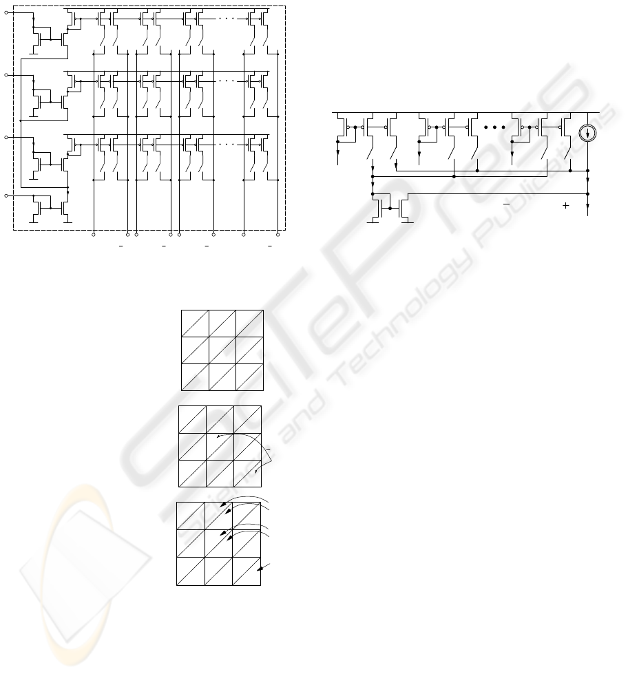
pixel block, which provides all necessary copies of
p
xyz
, is shown in Fig. 4. Particular branches
(connections) in this circuit are controlled using
configuration bits d
n,m,z,l
that are programmed off-
line. These bits establish only the connection map,
but values of the filter coefficients finally depend on
values of the currents I
h
.
)
I
DC
p
1
p
2
p
(+)
1
p
(-)
1
d
12
d
11
d
22
d
21
d
N
2
d
N
1
p
(+)
d
...1
p
(-)
d
...2
I
DC
p
N
ii
=
Σ
B
xy
()
Σ
ii
(
Figure 6: Calculation scheme of the output signal B
xy
.
It is convenient to collect the configuration bits d
into a single 4-dimensional matrix D, in which the
first two dimensions (n, m) are determined by
dimensions of the filter mask H. The 3
rd
dimension
(z) is determined by the length of the vector P
xy
, i.e.
by number of unique filter coefficients, while the 4
th
dimension is always equal to 2. Theoretically
products from a given vector P
xy
can be used in
calculation of n·m output samples. In this situation
bits that are under position n, m in the matrix D
determine how the products from this vector will be
used to calculate a given signal B
xy
. The 3
rd
dimension determines which product(s) from a given
vector P
xy
will be added to a given signal B
xy
, while
the last dimension determines if this product(s) will
be added with a positive or the negative value.
Taking this principle into account, an example
matrix D in case of the mask shown in Fig. 1 would
have dimensions 3, 3, 2, 2, so the total number of the
configuration bits d is in this case equal to only 36.
Several example connection maps for different
filter masks both the high-pass and the low-pass,
together with required currents representing
particular filter coefficients h
i
, are shown in Fig. 5.
In presented examples 2 unique filter coefficients are
assumed for simplicity.
It is worth noting that when two different filters
have an equal connection map and differ only by
value of selected coefficients then switching
between such filters requires only adjusting the
currents I
h
. It is also worth noting that although the
BIODEVICES 2009 - International Conference on Biomedical Electronics and Devices
48
number of coefficients in the vector h is usually low,
these coefficients can be combined together to
provide an effectively larger number of coefficients,
as in the example map shown in Fig. 5 (c).
Products p that are added as negative values are
summed in a separate junction, then inverted in a
single NMOS-type current mirror, and finally added
to the output signal, as shown in Fig 6. The potential
problem in this approach occurs when sum of the
negative values is larger than sum of the positive
values, which may turn off the output current mirror.
This problem has been solved by introducing an
additional constant current I
DC
, which can be
optionally added to the output signal in such a case.
3 CMOS IMPLEMENTATION OF
THE PARALLEL FILTER AND
EXPERIMENTAL RESULTS
An experimental image processing block has been
realized by authors in a 180 nm CMOS process. In
this prototype the image resolution is equal to 6 x 1
pixels, while the mask has dimensions 3 x 1. Such
parameters are sufficient to verify the concept, but as
the filter has a modular structure, higher resolutions
can be easily realized. For example, the filter with
8x8 pixels with 3x3 masks has been successfully
verified in the HSPICE simulations.
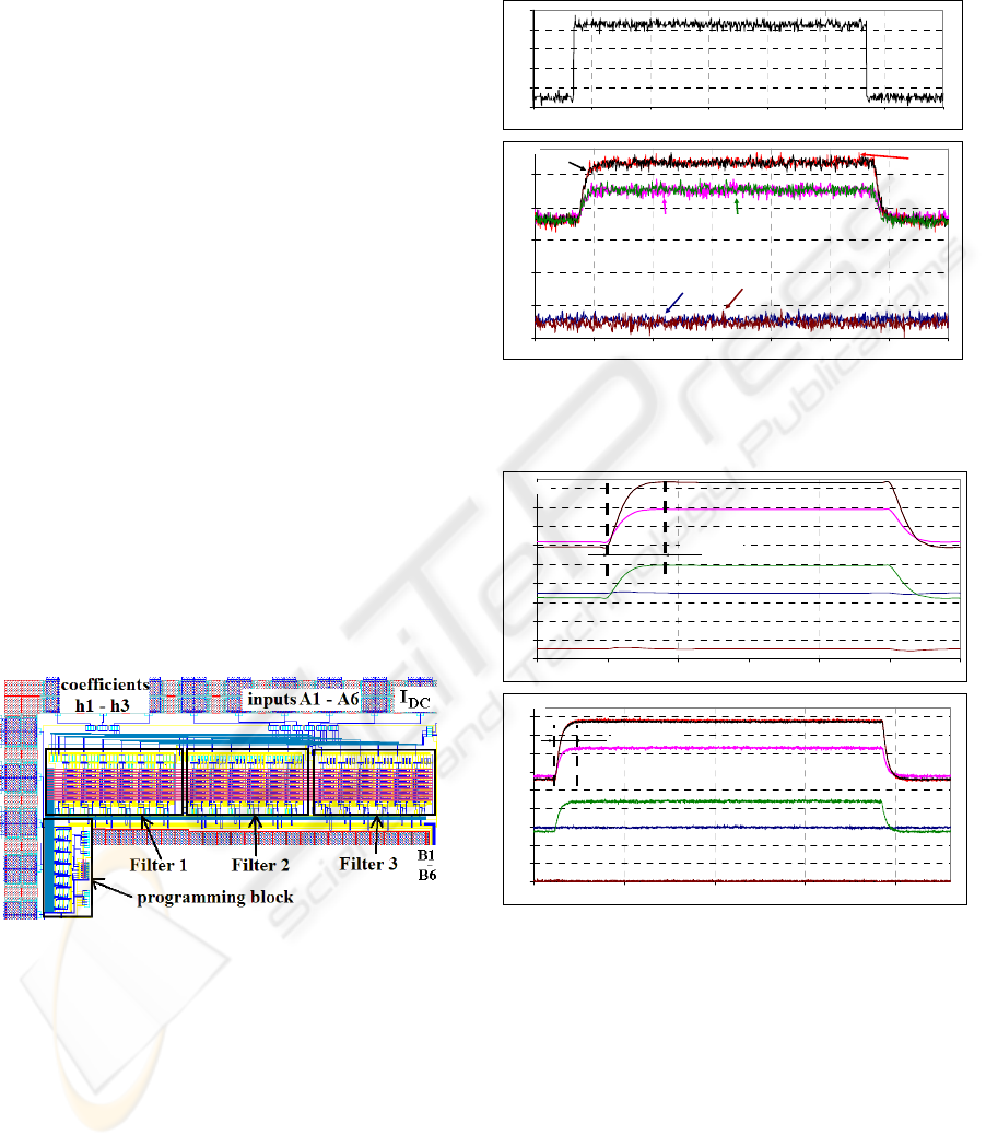
Figure 7: Experimental programmable image filter
realized in three versions with different transistor
dimensions.
The internal structure of the chip is shown in Fig.
7. The common problem in the Gilbert multipliers
used in the proposed filter, in which transistors
operate in weak inversion is influence of the
transistor mismatch on the filter accuracy. To verify
influence of this effect the experimental filter has
been designed in three versions that differ only in
the transistor dimensions (filter 1, filter 2, filter 3).
The measurement results show that mismatch has a
limited influence only on a DC value at particular
filter outputs, which can be easily corrected at the
digital side, after analog-to-digital conversion.
0.3
0.35
0.4
0.45
0.5
0.55
0.0008 0.0009 0.001 0.0011 0.0012 0.0013 0.0014 0.0015
0.105
0.11
0.115
0.12
0.125
0.13
0.0008 0.0009 0.001 0.0011 0.0012 0.0013 0.0014 0.0015
Time [s]
Vout [V]
B1 B6
B2 B5
B3
B4
Figure 8: Measurements for small signals for the low pass
filter (top) input signals A3 and A4 (bottom) the filter’s
outputs B1-B6. Results for are for the ‘filter 2’.
2.9
3.1
3.3
3.5
3.7
3.9
4.1
4.3
4.5
4.7
78910111213
Time [us]
I
out [uA]
B 3, B 4
B 2
B 5
B 1
B 6
T_ f < 1 us
0.3
0.32
0.34
0.36
0.38
0.4
0.42
0.44
0.46
0.48
0.0001 0.0006 0.0011 0.0016 0.0021
Time [s]
V
out [V]
T_ f = 0.1ms
B 5
B 6
B 1
B 2
B 3, B 4
Figure 9: Low pass filter (top) HSPICE postlayout
simulations and (bottom) the measurement results.
Selected measurement results and post-layout
simulations have been presented to demonstrate the
filter performance. The first and the second
experiments, shown in Figs. 8 and 9, are for lowpass
filter mask, H = [1, 1, 1] for small and for large input
signals respectively. Fig. 8 illustrates additionally
the input waveform applied to the A3 and A4 inputs.
The other inputs are constant and equal to the
bottom value of this pulse signal.
AN ASYNCHRONOUS PROGRAMMABLE PARALLEL 2-D IMAGE FILTER CMOS IC BASED ON THE GILBERT
VECTOR MULTIPLIER
49
2.9
3.1
3.3
3.5
3.7
3.9
4.1
4.3
4.5
4.7
7 8 9 10111213
Time [us]
I
out [uA]
B 3, B 4
B 2
B 5
B 1
B 6
T_ f < 1 us
0.3
0.32
0.34
0.36
0.38
0.4
0.42
0.44
0.46
0.48
0.0001 0.0006 0.0011 0.0016 0.0021
Time [s]
V
out [V]
T_ f = 0.1ms
B 5
B 6
B 1
B 2
B 3, B 4
Figure 10: High pass filter (top) HSPICE postlayout
simulations and (bottom) the measurement results.
Table 1: Example results for the low-pass filter [1,1,1]
(see Fig. 8).
Input [μA] A
1
A
2
A
3
A
4
A
5
A
6
2.5 2.5 5.098 5.098 2.5 2.5
Out [μA] B
1
B
2
B
3
B
4
B
5
B
6
calculated 3.880 4.461 4.757 4.757 4.176 3.595
simulated 3.595 4.475 4.761 4.761 3.885 3.002
measured 3.562 4.456 4.768 4.754 3.851 2.940
er_S/C % 15.68 0.77 0.22 0.22 16.03 32.60
er_M/C %
17.50 0.27 -0.60 0.20 17.88 36.03
er_M/S % -1.81 -1.04 0.39 -0.41 -1.86 3.43
Table 2: Example results for the high-pass filter [1,-1,1]
(see Fig. 9).
Input [μA] A
1
A
2
A
3
A
4
A
5
A
6
2.5 2.5 5.098 5.098 2.5 2.5
Out [μA] B
1
B
2
B
3
B
4
B
5
B
6
calculated
2.195 2.420 2.186 2.420 2.654 2.645
simulated
1.885 2.407 2.186 2.405 2.686 3.001
measured
1.969 2.416 2.184 2.402 2.643 2.913
er_S/C %
32.83 1.38 -0.01 1.63 -3.40 -37.7
er_M/C %
23.94 0.40 0.23 1.86 1.12 -28.4
er_M/S %
8.89 0.97 -0.24 -0.23 -4.52 -9.26
A detailed comparison for the experiment with
large input signals is provided in Table 1. To
investigate the dynamic parameters of the filter, the
input image, A, was varied during the test. The A
1
,
A
2
, A
5
and A
6
input samples were constant during the
test and equal to 2.5 μA, while the others (A
3
, A
4
)
were oscillating in the range between c.a. 2.19 and
5.1 μA. Theoretical (calculated), simulated and
measured values of the output pixels are given in the
4
th
, 5
th
and 6
th
rows respectively.
The results have been compared in terms of the
errors given in last three rows, in which S/C means
simulated vs. calculated results etc. All presented
results are for supply voltage 0.8 V.
The results for an example highpass filter with a
mask H = [-1 1 0] are shown in Fig. 10 and
compared in details in Table 2.
Notice that error values in signals B
2
-B
4
are
below 1-2 %. This is regularly observed for different
input images and filter masks. On the other hand,
errors concerning the B
1
, B
6
and for the low-pass
filter additionally B
5
outputs (due to A
6
being zeroed)
are larger, which is due to the border effect where
samples are calculated using only two inputs A
i
.
The noise at the output is at a level of 1 mV – the
currents are measured as voltages on 100 kΩ
resistors. The measured dynamic range depends on
the average value of the input pixels as well as on
type of the filter mask. The example measured
values are as follows:
a) for large signals (about 3 μA),
low pass filter SNR = 36dB (6 bits); see Fig. 9
b) for large signals (about 3 μA),
high pass filter SNR = 30dB (5 bits); see Fig. 10
c) for small signals (about 0.6 μA),
low pass filter SNR = 24dB (4 bits); see Fig. 8
d) for small signals (about 0.6 μA),
high pass filter SNR = 21dB (3 bits)
The maximum data rate depends on values of the
input signals and the transistors dimensions used in
GSVM circuits. The example data rates are as
follows:
a) filter 1 (W/L=15/5 μm)
is equal to 15.15 [kframes/s],
b) filter 2 (W/L=8/2 μm)
is equal to 21.74 [kframes/s],
c) filter 3 (W/L=6/1 μm)
is equal to 33.33 [kframes/s]
In our experimental filter each frame consists of
6 pixels. Power dissipation depends on values of the
input currents I
xy
. For small input values c. 0.6 μA
power dissipation is equal to 5 μW, while for larger
values c. 3 μA it equals to 30 μW.
It is worth noting that filter accuracy, which has
an influence on the gray scale depth, does not differ
significantly between the simulations and the
measurements, although the environmental noise
BIODEVICES 2009 - International Conference on Biomedical Electronics and Devices
50
limits the possible SNR. The noise is kept at a level
of 1 mV, which limits the filter accuracy by c. 6 dB
(1 bit). The accuracy is lower in case of high-pass
filters, which is due to additional signal inverting.
On the other hand the data rate significantly
differs between simulations and measurements. The
lower data rate attained in measurements is due to
large capacitances of pads as well as the setup
environment. The conclusion is that when the filter
is part of a bigger system, in which the output analog
signals are further processed in the chip, the data
rate can be higher and closer to the simulation
results. In this case energy dissipated per calculation
of a single pixel will be much smaller.
4 CONCLUSIONS
A 2-D analog, current-mode FIR filter has been
proposed in this paper. The main building block in
our filter is the Gilbert scalar-by-vector multiplier
that allows for an ultra-low power dissipation due to
transistors operating in weak inversion.
The proposed filter is a programmable solution,
with a very simple logic block and small number of
programming bits that allow for realization of
different filter masks both the high-pass and the low-
pass. One of the main advantages is a parallel and
asynchronous calculation of all output pixels without
using clock generators that typically are source of
feedthrough noise.
To verify the proposed idea, three experimental
image filters with different transistor dimensions
have been designed in a 180 nm CMOS technology.
Attenuation observed in post-layout HSPICE
simulations reaches a level of about 55 dB.
Theoretical analysis and measurement results
concerning the influence of the transistor-threshold-
voltage mismatch on the filter properties shows that
even in the worst case scenario, attenuation higher
than 36-dB (6 bits) can be achieved, for the
mismatch that is at the level of 2-3 %, which is
sufficient for many practical applications e.g. in
endoscopic capsules. The attained lower attenuation
is caused by an environmental noise that is present
in the input signal, as shown in Fig. 8 (top).
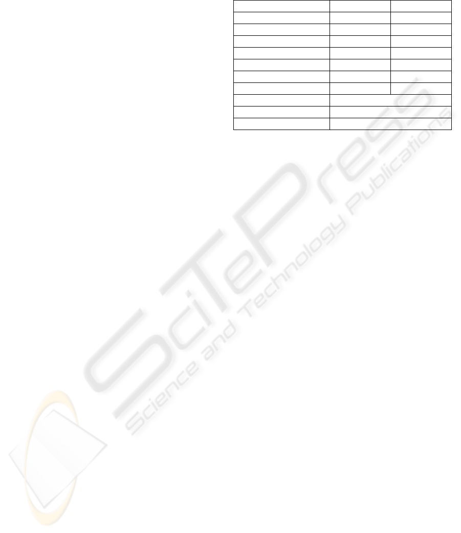
The filter performance is summarized in Table 3.
The data rate is given in image frames/s as in our
proposed filter this parameter does not depend on
number of pixels in a single frame. The data rate
attained in measurement significantly exceeds those
usually required is endoscopic capsules i.e. several
frames/s (Xie et al., 2006). This creates the
possibility to switch off the circuit for most of the
time and to save energy, which is one of the key
criteria in wireless endoscopic capsules.
Table 3: Summary of the image filters performance.
Parameter Small signals Large signals
Voltage supply 0.8 V 0.8 V
effective data rate(measur.) 15 kframes/s 15 kframes/s
effective data rate(simulate.) 350 kframes/s 1 Mframes/s
SNR (dB) 21-24 (3-4 bits) 30-36 (5-6 bits)
Power dissipation (6 pixels) 5 μW 30 μW
Energy/pixel (measured) 55 pJ 250 pJ
Energy/pixel (simulated) 2.3 pJ 5 pJ
Process TSMC CMOS 0.18 μm
Die area - one filter: 6 pixels 350 x 150 μm (0.052 mm
2
)
Image/mask resolution 6 x 1 / 3 x 1
ACKNOWLEDGEMENTS
The work is supported by EU Marie Curie Outgoing
International Fellowship No.
021926
REFERENCES
Meng, M.Q.-H. Tao Mei, Jiexin Pu, Chao Hu, Xiaona
Wang, Yawen Chan, “Wireless robotic capsule
endoscopy: state-of-the-art and challenges”, 5th World
Congress on Intelligent Control and Automation
(WCICA), 2004, Vol. 6, June 2004, pp.5561 - 5555
X. Xie, G. Li, X. Chen, X. Li, Z. Wang, “A Low-Power
Digital IC Design Inside the Wireless Endoscopic
Capsule”, IEEE Journal of Solid-State Circuits, Vol.
41, Issue 11, Nov. 2006, pp. 2390 - 2400
Shaou-Gang Miaou, Shih-Tse Chen, Fu-Sheng Ke,
“Capsule endoscopy image coding using wavelet-
based adaptive vector quantization without codebook
training”, 3rd International Conference on Information
Technology and Applications (ICITA), Vol. 1, July
2005, pp. 634 - 637
C. Winstead, Analog Iterative Error Control Decoders,
Ph.D disserta-tion, University of Alberta, ECE
Department, Edmonton, ABa, 2004.
G. Linan, P. Foldesy, S. Espejo, R. Dominguez-Castro, A.
Rodriguez-Vazquez, “A 0.5µm CMOS 106 transistors
analog programmable array processor for real–time
image processing”, 25th European Solid-State Circuits
Conference (ESSCIRC), 1999, pp. 358-361.
R. Serrano-Gotarredona, T. Serrano-Gotarredona, A.
Acosta-Jimenez, C. Serrano-Gotarredona, J. A. Perez-
Carrasco, A. Linares-Barranco, G. Jimenez-Moreno,
A. Civit-Ballcels, and B. Linares-Barranco, "On Real-
Time AER 2D Convolutions Hardware for
Neuromorphic Spike Based Cortical Processing,"
IEEE Trans. on Neural Networks, vol.19, No.7, pp.
1196-1219, July 2008
AN ASYNCHRONOUS PROGRAMMABLE PARALLEL 2-D IMAGE FILTER CMOS IC BASED ON THE GILBERT
VECTOR MULTIPLIER
51
