
3-((2′:2″,5″:2′′′-TERTHIOPHENE)-3″-YL) ACRYLIC ACID AS
ORGANIC FIELD EFFECT TRANSISTOR FOR DNA SENSING
K. C. Aw
1
, N. Tjitra Salim
2
, H. Peng
3
, J. Travas-Sedjic
3
and W. Gao
2
1
Mechanical Engineering
2
Chemical and Materials Engineering
3
Chemistry
The University of Auckland, New Zealand
Keywords: 3-((2′:2″,5″:2′′′-terthiophene)-3″-yl) acrylic acid, DNA sensor, Organic field effect transistor.
Abstract: The aim of this paper is to demonstrate the use of organic field effect transistor (OFET) as a DNA sensor.
We have synthesized a functionalised terthiophene monomer 3-((2′:2″,5″:2′′′-terthiophene)-3″-yl) acrylic
acid (TAA) and has been successfully electrodeposited as an active layer of an OFET. The polymer was
oxidised in order to increase its conductivity. A mobility of 0.25 cm
2
/V.s was achieved with an oxidising
potential of 0.9 V. A preliminary DNA sensing test was performed on the OFET with poly TAA as active
layer and a shift in threshold voltage was observed after DNA immobilization and hybridization, showing
its potential as DNA sensor.
1 INTRODUCTION
Previous studies (Peng, Zhang, Spires et al l, 2007;
Zhang, Peng, Kilmartin et al, 2007) have shown the
ability of the acid-functionalised conducting
polymers to detect DNA hybridization, where
carboxylic acidic functionality enabled covalent
attachment of biomolecules such as DNA
(oligonucleotides).
However, in this research the DNA detection
will be based on an organic field effect transistor
(OFET) device instead of the change in impedance
of an organic thin film as in Refs 1 and 2. The
OFET device as a sensor can be more sensitive due
to the ability to control OFET conduction via a third
terminal called “gate”.
2 EXPERIMENT PROCEDURES
The synthesis of 3-((2′:2″,5″:2′′′-terthiophene)-3″-
yl) acrylic acid (TAA) monomer is based on work
by (Peng et al, 2007). The monomers were
electropolymerized on a prefabricated substrate
consisting of a source (S), a drain (D) and a gate (G)
terminals. The bottom gate was a highly doped Si
and a 100 nm SiO
2
acted as the gate dielectric.
Finally, the two gold contacts as S and D with an
effective channel width of 5560 μm were patterned
on top of the SiO
2
. Channel length spacing of 25,
was used. The schematic structure of the OFET is
illustrated in Figure 1.
n
+
- Si
SiO
2
SD
PTAA
Figure 1: The schematic structure of bottom contact,
bottom gate PTAA-based OFET.
The electropolymerisation was performed using
the cyclic voltammetry from 0 to 1.3 V at scan rate
of 50 mV/s by a CH Instrument electrochemical
workstation (Model 440, CH Instruments, USA).
The gold S and D contacts on the substrate were
used as the working electrodes during
electropolymerisation. A Pt wire and Ag/AgCl (3 M
KCl) were used as the counter electrode and the
reference electrode, respectively. The
polymerisation solution comprised of 0.05 M
tetrabutylammonium trifluoromethanesulfonate and
0.005 M TAA in acetonitrile. The obtained polymer
159
Aw K., Tjitra Salim N., Peng H., Travas-Sedjic J. and Gao W. (2010).
3-((2’:2",5":2”’-TERTHIOPHENE)-3"-YL) ACRYLIC ACID AS ORGANIC FIELD EFFECT TRANSISTOR FOR DNA SENSING.
In Proceedings of the Third International Conference on Biomedical Electronics and Devices, pages 159-162
DOI: 10.5220/0002692601590162
Copyright
c
SciTePress

TAA (PTAA) film was then oxidised in a monomer
free solution by a constant potential method for 5
minutes to achieve different doping levels, therefore
different conductivities. Five oxidising potential
(V
OX
) of 0.1, 0.2, 0.6, 0.9 and 1.1 V were chosen to
investigate their effect on the performance of the
fabricated OFET. The arrangement for
electropolymerization is shown in Figure 2.
CH Instruments
Model 440
V
Working electrode
(S & D contacts)
Counter electrode
(Pt wire)
Reference electrode
(Ag/AgCl/3M KCl)
Figure 2: The electrodes arrangement for electro
polymerization.
The OFET electrical characteristic was measured
using Keithley 2602 source measure unit after the
doping process. The microstructure of PTAA film
on the Si substrate was examined using the scanning
electron microscope (SEM).
Following the optimisation of PTAA-OFET
fabrication process, DNA sensing ability of this
OFET was tested. The study starts with DNA
immobilization, a process where single stranded
DNA (ssDNA) molecules with known sequence
(NH
2
-GAT GAG TAT TGA TGC CGA-3)
synthesized by Invitrogen Life Technologies are
covalently attached to the PTAA film. To attach the
ssDNA, a 40 μL of phosphate buffer (pH 5.2)
containing 20 nmol ssDNA probe and 400 nmol 1-
ethyl-3-(3-dimethylaminopropyl)carbodiimide
(EDC) was applied on the surface of PTAA-OFET
and was kept at 28 °C for 1 h. Finally, the OFET
was thoroughly washed using phosphate buffered
saline (PBS) solution (pH 7.4) to remove any
unattached ssDNA. After immobilization, the I-V
characteristics of PTAA-OFET were measured using
Keithley 2602 source measure unit.
The next step to test the sensing ability of
PTAA-OFET is DNA hybridization, where the
complementary ssDNA is applied to the surface of
OFET and hybridizes with the immobilized ssDNA
via complementary base pairing to form a double
helix DNA. The hybridization was carried out by
incubating the PTAA-OFET with immobilized DNA
in PBS solution containing complementary ssDNA
samples for 1 h at 42 °C. After hybridization, the
OFET was washed three times using PBS solution to
remove any non-hybridised ssDNA. Then I-V
characterisations were carried out to determine the
effect of hybridization on the OFET performance.
3 RESULTS AND DISCUSSIONS
The PTAA-OFET was electrically characterized for
diferenct V
OX
and highest calculated carrier mobility
of 0.25 cm
2
/V.s at V
D,sat
= -20 V is achieved with
V
OX
= 0.9 V and threshold voltage (V
T
) of
approximately 7 V (Tjitra Salim, Aw, Peng, et. al.,
2008). Figure 3 show the OFET characteristics of
PTAA oxidised at 0.9 V where the highest carrier
mobility was achieved. The I-V characteristic is not
of good quality due to the fact that
electropolymerization process could produce film
with high structural and conjugation defects
(Roncali, 1992)
The above-mentioned results are in good
accordance with the cyclic voltammogram (CV) of
PTAA obtained in a monomer free solution as
shown in Figure 4. From this CV, two anodic peaks
at +0.6 V (A) and +1.05 V (B) are observed. The
first anodic peak marks the beginning of polymer
oxidation, indicating the formation of polaron and
subsequent bipolaron formation, i.e. the charge
carrier (holes) (Chen and Inganas, 1996). Therefore,
one can see that the PTAA film is in a neutral state
with low charge carriers (holes) density when V
OX
<
0.6 V. With increasing V
OX
, the PTAA starts to be
oxidised, increasing the charge carrier density,
which in turn would increase its conductivity. A
higher conductivity PTAA film as an active layer is
considered to be responsible for the increase in
μ
of
an OFET. When V
OX
≥ +1.05 V (at the second
anodic peak), a strong increase in the anodic current
is observed, indicating the beginning of polymer
oxidative degradation. This explains the low
transistor performance when PTAA as an active
layer was oxidised at voltage greater than 1 V.
BIODEVICES 2010 - International Conference on Biomedical Electronics and Devices
160
-9.00E-06
-8.00E-06
-7.00E-06
-6.00E-06
-5.00E-06
-4.00E-06
-3.00E-06
-2.00E-06
-1.00E-06
0.00E+00
-20-15-10-5
V
D
(V)
I
D
(A)
V
G
= 0 V
V
G
= -10 V
V
G
= -11 V
V
G
= -12 V
V
G
= -13 V
V
G
=-14V
V
G
= -15 V
(a)
1.00E-08
1.00E-07
1.00E-06
1.00E-05
-15 -10 -5 0
V
G
(V)
-I
D
(A)
0
0.0005
0.001
0.0015
0.002
0.0025
0.003
0.0035
0.004
(-I
D
)
1/2
(A
1/2
)
(b)
V
D,sat
= -20 V
Figure 3: The I-V characteristics of bottom contact,
bottom gate PTAA-based OFET with VOX = 0.9 V; (a).
Output curves (ID-VD) at different gate voltages; and (b).
Transfer curves (ID-VG) in saturated regime at constant
source-drain voltage of -20 V (left scale) and square root
of the absolute value of ID as a function of VG (right
scale).
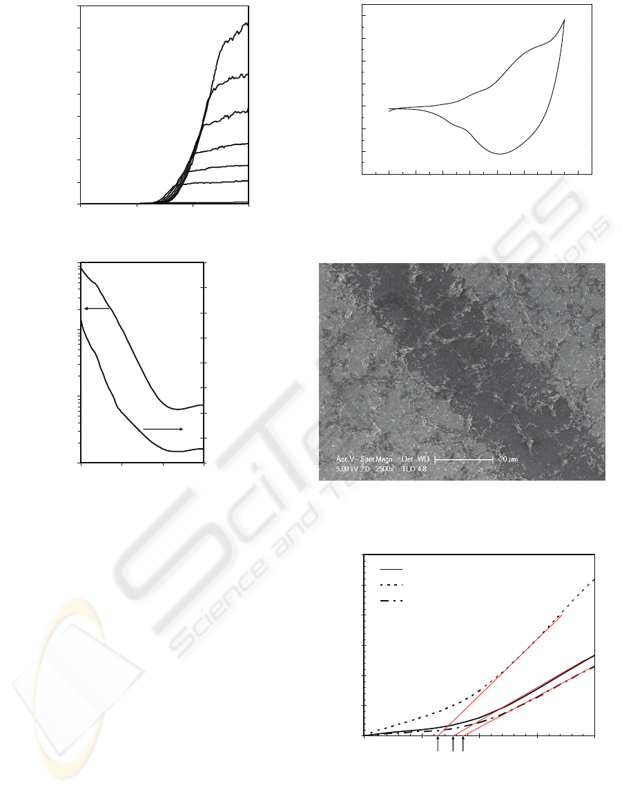
The morphology of PTAA film on top of gold (S
and D) contacts and across the channel is shown in
Figure 5, demonstrating that the electrodeposition of
PAA enables the creation of active region between
the S and D contacts creating an OFET.
A preliminary DNA sensing ability of PTAA-OFET
was tested and the results are shown in Figure 6. A
shift in threshold voltage (VT) was observed after
DNA immobilization and hybridization of
complementary DNA, confirming the sensing ability
of PTAA-OFET. Initially, the PTAA-OFET
obtained a threshold voltage (VT,i) of -8 V and after
DNA immobilization, the threshold voltage has
shifted to about -6 V (VT,im). This positive VT shift
is expected as the phosphate groups on the DNA
-0.2 0.0 0.2 0.4 0.6 0.8 1.0 1.2 1.4
-15
-10
-5
0
5
10
15
20
Current (μA)
Potential (V)
A
A'
B
B'
Figure 4: The cyclic voltammogram (CV) of PTAA film
in a monomer free solution with a scan rate of 50 mV/s.
Figure 5: SEM images showing the morphology of PTAA
film on top of the gold (S and D) contacts and across the
channel.
0
0.001
0.002
0.003
0.004
0.005
0.006
-20-15-10-50
V
G
(
V
)
(-I
D
)
1/2
(A)
1/2
Initial - before immobilisation
Immobilised
Hybridised - complementary
V
T, i
V
T,im
V
T,h
V
D,sat
= -20 V
Figure 6: The √ID vs VG at VD,sat = -20 V showing the
threshold voltages (VT) of bare PTAA-OFET,
immobilized PTAA-OFET and hybridized PTAA-OFET
with complementary DNA.
S
Channel
Region
D
3-((2':2",5":2'''-TERTHIOPHENE)-3"-YL) ACRYLIC ACID AS ORGANIC FIELD EFFECT TRANSISTOR FOR DNA
SENSING
161

backbone are able to attract electrons from the
organic semiconductor, increasing the hole
concentration of PTAA than before DNA
immobilization (Zhang and Subramanian, 2007).
The increased in holes concentration would result in
the shift of V
T
to a lower negative voltage (positive
shift), causing an effective p-doping of PTAA.
After the hybridization with complementary
DNA, the threshold voltage (V
T
) shifted more
negatively (negative shift) to approximately -9 V.
Hybridization with complementary DNA would
result in double stranded DNA (dsDNA), where the
bases of two complementary single stranded DNA
(ssDNA) would pair up and form the double helix.
According to (Zhang and Subramanian, 2007),
dsDNA molecules could not be immobilized
(attached) to the organic semiconductor (PTAA) as
effectively as ssDNA molecules. This would result
in less interaction between DNA backbone and
PTAA that are known to be able to attract electrons,
lowering the holes concentration in PTAA and
hence, increasing the OFET’s V
T
to be more
negative. The low interaction ability between
dsDNA and PTAA is because the bases of DNA are
not exposed in dsDNA. The bases of DNA are
responsible to the hybrophobic interaction, resulting
in physical adsorption between ssDNA and PTAA,
i.e. immobilization of ssDNA.
4 CONCLUSIONS
The PTAA based p-channel OFETs were fabricated
successfully with a μmax of 0.25 cm
2
/Vs. The
amount of doping through the V
OX
in PTAA is
crucial in controlling the μ of the OFET. An
optimum V
OX
of 0.9 V was obtained, producing
OFET with the highest μ. A V
OX
> 1.0 V causes
degradation to the PTAA film, leading to poor
charge mobility, while V
OX
≤ 0.2 V does not
produce sufficient doping. These results
demonstrated that the μ of FET fabricated with
PTAA can be controlled by V
OX
and correlates with
the potential value of the cyclic voltammogram for
0.2 V ≤ V
OX
< 1.1 V. A preliminary DNA sensing
test was performed on the PTAA-OFET and a shift
in threshold voltage was observed after DNA
immobilisation and hybridisation, showing its
potential as DNA sensor. However, more detailed
study is required to realise this PTAA-OFET as
DNA sensor before it can be deployed.
REFERENCES
Chen, X., Inganas, O., 1996. Three-Step Redox in
Polythiophenes: Evidence from
Electrochemistry at an Ultramicroelectrode, The
Journal of Physical Chemistry 100 (37), 15202-15206.
Peng,H., Zhang, L., Spires, J. et al., 2007. Synthesis of a
functionalized polythiophene as an active substrate for
a label-free electrochemical genosensor, Polymer 48
(12), 3413-3419.
Roncali, J., 1992. Conjugated poly(thiophenes): Synthesis,
functionalization and applications, Chemical Reviews
92 (12), 711.
Tjitra Salim, N., Aw K.C., Peng, H. et. al., 2008. New 3-
((2':2'',5'':2'''-terthiophene)-3''-yl) acrylic acid as active
layer for organic field-effect transistor, Materials
Chemistry and Physics, 111 (1), 1-4.
Zhang, L., Peng, H., Kilmartin, P.A. et al., 2007.
Polymeric Acid Doped Polyaniline Nanotubes for
Oligonucleotide Sensors, Electroanalysis 19 (7-8),
870-875.
Zhang Q., Subramanian, V., 2007. DNA hybridization
detection with organic thin film transistors: Toward
fast and disposable DNA microarray chips, Biosensors
and Bioelectronics 22 (12), 3182-3187.
BIODEVICES 2010 - International Conference on Biomedical Electronics and Devices
162
