
ELECTRICAL CHARACTERIZATION OF
SEQUENCE-SPECIFIC LABEL-FREE DNA BY USING
POLYSILICON WIRE
You-Lin Wu, Po-Yen Hsu
Department of Electrical Engineering, National Chi Nan University, Puli, Nantou, Taiwan
Chung-Ping Hsu
Division of Chest Surgery, Department of Surgery, Taichung Veterans General Hospital, Taichung, Taiwan
Wen- Cheng Liu
Graduate Institute of Biomedicine and Biomedical, National Chi Nan University, Puli, Nantou, Taiwan
Keywords: DNA bases detection, Polysilicon wire sensor, Label-free.
Abstract: In this paper we report the electrical measurement of sequence-specific and label-free deoxyribonucleic acid
(DNA) by using poly-silicon (poly-Si) wire. Four single-strained (ss) DNA bases, adenine (A), thymine (T),
cytosine (C) and guanines (G), as well as double-stranded (ds) DNA sequences, ds(A-T) and ds(C-G), with
different lengths and concentrations were dropped onto the poly-Si wire surface, and currents flowing
through the poly-Si wire channel were determined. It is found that the amount change of the channel current
ΔI for ssDNAs with fixed length and fixed concentration is that T > C > G > A. For dsDNA sequence, we
observe that ds(A-T) has higher ΔI than does ds(C-G). We also prove that single base change in ssDNA is
feasible by using the poly-Si wire sensor.
1 INTRODUCTION
Determination of DNA bases has long been an
intensive research topic in biotechnology and
medical diagnostics since the genetic information
carried by an organism is inscribed in DNA. On the
other hand, measurements of DNA conductivity,
hybridization and melting using electronic means
have also drawn much attention in recent years due
to the possible applications in molecular electronics.
Typically, the detection of DNA uses techniques
such as radiochemical, enzymatic and fluorescent
(Lander, 1999) (Wang, 2000) based on detecting
different labels or reagents added in the molecules
under test. These techniques, however, are proven to
be time-consuming, expensive and complicated to
implement. Therefore, label-free DNA detection
methods such as cyclovoltametry and
chronopotentiometry have also been developed
(Mastrangelo, 1999) (de-los-Snatos-Alvarez et al,
2004). However, all these methods are wet type in
which the sensor has to be immersed in the solution
under test, and the selectivity as well as the detection
limit would not be accurate enough owing to the
influences of thermal drift of the electrolyte solution.
Thanks to the rapid progress in semiconductor
processing and nanofabrication techniques, many
semiconductor/nano electronic devices and nano-
scale measurement tools have been developed either
to measure the electrical properties of DNA or for
DNA detection. For example, Storm and his co-
workers used nanogap junctions to measure the
electrical resistance of hybridized and denatured
DNA molecules (Storm et al, 2001). Xu et al. (2007)
measured the conductance of DNA by using
scanning probe microscopy. On the other hand, field
effect devices such as electrolyte-insulator-silicon
(Fritz et al, 2002) and silicon nanowire (SiNW)
(Hahm and Lieber, 2001) have also been proposed
for the detection of hybridyzation and mutation of
170
Wu Y., Hsu P., Hsu C. and Liu W. (2010).
ELECTRICAL CHARACTERIZATION OF SEQUENCE-SPECIFIC LABEL-FREE DNA BY USING POLYSILICON WIRE.
In Proceedings of the Third International Conference on Biomedical Electronics and Devices, pages 170-173
DOI: 10.5220/0002712601700173
Copyright
c
SciTePress
DNAs. Instead of using SiNW, in this work we used
poly-Si wire for sequence-specific ssDNAs as well
as ds DNAs, A, T, C, G, A-T and C-G, detection
from the consideration of simplicity, economy and
easy-fabrication. In the present work, current
flowing through the poly-Si wire channel rather than
time-dependent conductance was determined. We
found that the amount of current change before and
after dropping the DNA solution under test on the
poly-Si wire surface is different for each ssDNA and
dsDNA. This result indicates that each of ssDNAs
and dsDNAs has its own characteristic amount of
current changes, and the poly-Si wire sensor can be
used as a promising DNA detection device.
2 EXPERIMENTS
In this work, p-type (100) Si wafer was used as the
substrate. After standard RCA cleaning, a 12 nm-
thick thermal oxide was grown at 900℃. Following
that, a phosphorous-doped polysilicon layer with a
thickness of 80 nm was deposited at 620℃ by
vertical furnace and having a sheet resistance of 40-
50 Ω/□. An e-beam writer was then used to define
the pattern of the poly-Si wire. After development,
the poly-Si wire was obtained by reactive-ion-
etching. The line width and length of the poly-Si
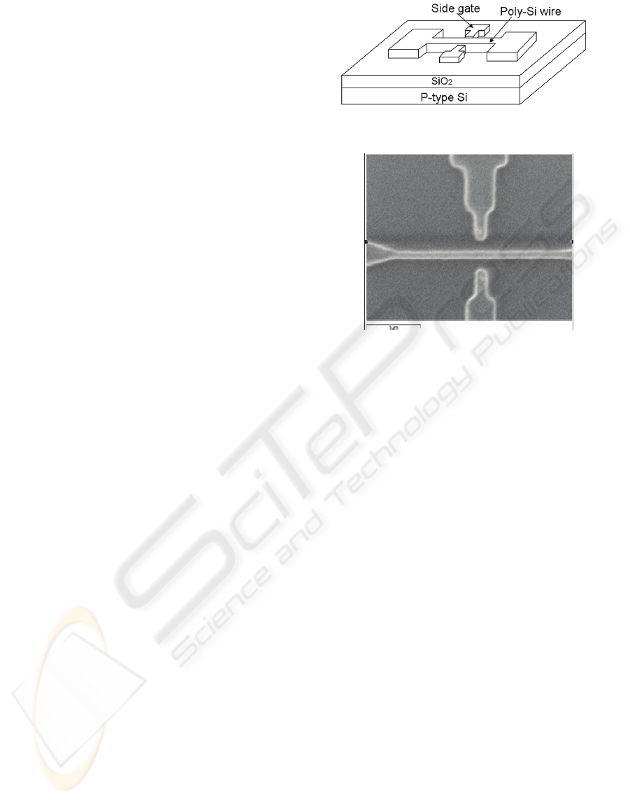
wire is about 200nm and 2um, respectively. Figure 1
and Figure 2 depicts respectively the schematic
diagram and the SEM image of the poly-Si wire
sensor used in this work. To increase the detection
sensitivity, an enzyme layer (γ-APTES) is deposited
onto the poly-Si wire surface and then cured at
120℃ for 5 min on a hot plate, which can enhance
the adhesion of DNA molecular with the poly-Si
wire surface as well as increase the sensitivity of the
sensor. The same sensor has been reported being
successfully used for cancer cells detection (Wu et al,
2008). In this work, the sensor was used for DNA
detection.
Sequence-specific DNA reagents (Invitrogen,
U.S.A.), ssA, ssT, ssC, ssG, ds(A-T) and ds(C-G),
with different concentrations (50, 100 nM) and
lengths (10, 20 mer) were prepared and dissolved in
a 0.165 M phosphate buffer solution. The DNA
solution under test was then dropped onto the poly-
Si wire sensor surface by using a micropipette. A
voltage was applied between the source and the
drain of the poly-Si wire without side gate bias, and
the current flowing through the poly-Si wire was
measured by using the semiconductor parameter
analyzer HP 4156B. All the experiments were
carried out at room temperature.
Figure 1: Schematic diagram of the poly-Si wire biosensor.
Figure 2: SEM picture of the Poly-Si wire, the line width
and length are about 200nm and 2um, respectively.
3 RESULTS AND DISCUSSION
Figure 3 and Fig. 4 show respectively the I-V
characteristics of 50 nM and 100 nM ssA, ssT, ssC
and ssG, with different lengths under forward bias.
As observed, the current I
DS
flowing through the
poly-Si wire increases with increasing source-drain
voltage V
DS
. It is interesting to note that the current
flowing through the poly-Si wire channel after the
solution under test was dropped onto the poly-Si
wire surface is higher than that before it was
dropped for all the sequence-specific ssDNAs except
for ssC. This result indicates that the polarity of the
surface charge of ssC is opposite to that of other ss
DNAs. Figure 5 compares the absolute value of the
amount of current changes (which is defined as ΔI
=⎥ I
DS
(after dropping) – I
DS
(before dropping)︳) of
ssA, ssT, ssC and ssG DNA with different
concentrations and lengths measured at V
DS
= 5V.
We find that ΔI increases with increasing DNA
length as well as concentration as expected because
the longer length and the higher concentration of
ssDNA, the more charges within the poly-Si wire
channel will be induced. We also observe that, for
the same length and concentration of ssDNA, the
amount of current changes ΔI is that T > C> G > A.
It is reported that the Fermi level of DNA bases is
that T < C < G < A (Zwolak and Di Ventra, 2008).
Therefore, we believe that the surface charge of the
ELECTRICAL CHARACTERIZATION OF SEQUENCE-SPECIFIC LABEL-FREE DNA BY USING POLYSILICON
WIRE
171
poly-Si wire is modified by the electron transfer
between the wire surface and the DNA bases
attached.
Figure 3: I-V characteristics of the poly-Si wire after
dropping different 50 nM sequence-specific ssDNA
solution with a length of 10 mer and 20 mer.
Figure 4: I-V characteristics of the poly-Si wire after
dropping different 100 nM sequence-specific ssDNA
solution with a length of 10 mer and 20 mer.
Figure 5: Current difference comparison of ssA, ssT, ssC
and ssG with different concentrations and lengths
measured at V
DS
= 5V.
Figures 6 and 7 show respectively the I-V
characteristics of 50 nM and 100 nM sequence-
specific dsDNAs, ds(A-T) and ds(C-G) with
different lengths under forward bias. As observed,
ds(A-T) has higher I
DS
than ds(C-G) does. Since the
charge polarity of C is opposite to that of A, T and G,
it is believed that the net surface charge is reduced
when ds(C-G) is dropped onto the poly-Si wire
surface and would reduce the amount of induced
charge in the poly-Si wire channel, hence less
current would flow. Figure 8 compares the ΔI for the
all the dsDNA s and ssDNAs. It is reported that the
ds(C-G) and ds(A-T) might be treated respectively
as p-type and n-type semiconductor (Kim et al,
2006), which also explains the ΔI difference in Fig.
8. The detection of single base change in ssDNA
was also conducted in this work. The result (not
shown) indicates that the poly-Si wire sensor can be
used for the detection of single base change in
ssDNA.
Figure 6: I-V characteristics of the poly-Si wire after
dropping different 50 nM sequence-specific dsDNA
solution with a length of 10 mer and 20 mer.
Figure 7: I-V characteristics of the poly-Si wire after
dropping different 100 nM sequence-specific dsDNA
solution with a length of 10 mer and 20 mer.
BIODEVICES 2010 - International Conference on Biomedical Electronics and Devices
172
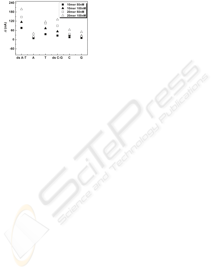
Figure 8: Current difference comparison of ssA, ssT, ssC,
ssG, ds(A-T) and ds(C-G) with different concentrations
and lengths measured at V
DS
= 5V.
4 CONCLUSIONS
In this paper we report the detection of ssDNAs and
dsDNAs with specific sequence by using the poly-Si
wire sensor. For ssDNA, we find that each ss DNA
base has its own characteristic ΔI, and the amount
changes of the current flowing through the poly-Si
wire is that T > C > G > A. For dsDNAs, we also
observed that ds(A-T) has higher ΔI than ds(C-G).
Our experimental result confirms that the surface
charge state is modified after the DNA solution is
dropped, which is believed to be related to the Fermi
levels of the DNA bases. We also prove that the
poly-Si wire sensor can be used for the detection of
single base change in ssDNA. In conclusion, the
poly-Si wire sensor can be used as a promising DNA
detection device.
ACKNOWLEDGEMENTS
This work is supported by the Taichung Veterans
General Hospital-National Chi Nan University Joint
Research Program no.TCVGH-NCNU987910.
REFERENCES
de-los-Snatos-Alvarez, P., Lobo-Castanon M. Juses,
Miranda-Ordieres, A. J., Tunon-Blanco, (2004).
Current strategies for electrochemical detection of
DNA with solid electrodes. Anal. Bioanal.Chem., 378,
104-118.
Fritz, J., Cooper, E. B., Gaudet, S., Sorger, P. K. Manalis,
S. R. (2002). Electronic detection of DNA by its
intrinsic molecular charge. Proc. Natl. Acad. Sci.
U.S.A., 99, 14142-14146.
Hahm, J. I., & Lieber, C. M. (2001). Direct ultrasensitive
electrical detection of DNA and DNA sequence
variations using nanowire nanosensors. Nano lett., 4,
51-54.
Kim, K. S., Ahn, S. K., Lee, Y., Lee, J. M., Roh, Y. (2006).
Effects of gate voltage on the characteristics of source-
drain current formed through DNA molecules. Thin
Solid Films, 515, 822-826.
Lander, E. S. (1999). Array of hope. Nat Genet. 21, 3-4.
Mastrangelo, C. H., (1999). DNA analysis system on a
chip. Solid-State Chemical and Biochemical Sensors,
Techna Faenza., 495-476.
Storm, A. J., van Noort, J., de Vries, S. Dekker, C. (2001).
Insulating behaviour for DNA molecules between
nanoelectrodes at the 100nm length scale. Appl. Phys.
Lett., 79, 3881.
Wang, J. (2000). Towards Genoelectronics:
Electrochemical Biosensing of DNA Hybridization
Chem. Eur. J., 5, 1681-1685.
Wu, Y. L., Hsu, P. Y., Hu, S. H., Hung, W. C., Lin, S. T.,
Hsu, C. P., Cullis, A. G. (2008). Polysilicon Wire
Sensor for Biochemical Detection with The Help of
Capillary Atomic-Force-Microscopy Tip for Solution
Transfer. 9
th
International conference on Solid State
and Integrated Circuit technology. IEEE press.
Xu, M., Endres, R. Arakawa, G., Y. (2007). The
Electronic Properties of DNA bases, Small, 3, 1539-
1543.
Zwolak, M., Di Ventra, M., (2008). Colloquium: Physical
approaches to DNA sequencing and detection. Rev.
Mod. Phys., 80, 141-165.
ELECTRICAL CHARACTERIZATION OF SEQUENCE-SPECIFIC LABEL-FREE DNA BY USING POLYSILICON
WIRE
173
