
AN
ELECTRONIC INTERFACE FOR NEURAL ACTIVITY
RECORDING AND STIMULATION
Gianmarco Angius, Caterina Carboni, Daniela Loi and Massimo Barbaro
Department of Electrical and Electronic Engineering, University of Cagliari, Piazza d’Armi, Cagliari, Italy
Keywords:
Neural extracellular recording, Neural Stimulation, Neural signal processing.
Abstract:
A portable neural activity acquisition and stimulation system by means of tfLIFE implantable electrodes has
been realized. The detecting circuit provides: a selective filtering made up of a 4th order high pass Multiple
Feedback filter ( f
−3dB
= 1.1kHz) and a 4th order low pass Multiple Feedback filter ( f
−3dB
= 2kHz), a variable
gain (24dB - 44dB) and a 16 bit analog to digital conversion. The stimulator allows to generate specific
electrical signals through a digital-to-analog converter while stimulation parameters as frequency, duration
and intensity are controlled by a digital microcontroller. Simulation results and first experimental results of
the interface demonstrate how neural signals of a few of microvolts can be filtered, programmable amplified
and digitalized without distortion.
1 INTRODUCTION
In recent years there has been an explosion of in-
terest in the development of technologies whose end
goal is to analyze the human nervous system and in
particular, the correlation between the neural activ-
ity and specific cognitive, sensory and motor func-
tions (Wessberg et al., 2000; Salzman and Newsome,
1994). Recent developments in microelectronic sys-
tem technology have made easier the design of neural-
controlled interfaces by means of appropriate elec-
trodes which allow a selective link with the peripheral
nervous system (PNS). A major problem in such ap-
plications is the morphology of the signals to record.
As a matter of fact, extracellular neural signals (ENG)
are characterized by a low-amplitude signal (in the
order of microvolts) and low-frequency bandwidth
(main energy spectrum concentrated close to 2kHz).
The acquisition of this kind of signals is therefore
affected by noise, mainly due to electro-myographic
signals (EMG) interference and to biological envi-
ronment (Wang et al., 2005; Watkins et al., 2006).
EMG signals have an amplitude of the order of mil-
livolts (several orders of magnitude greater than use-
ful ones) but are limited in frequency below 300Hz.
Low-noise amplification and selective filtering repre-
sent then the two basic operations of any recording
circuit proposed in the past (Obeid et al., 2004; Gos-
selin and Sawan, 2005; Jochum et al., 2009). This
work presents the design and test of a low power elec-
tronic neural system which allows a bi-directional in-
teraction between the brain and “smart” artificial de-
vices. The main goal was to realize a portable, eas-
ily reproducible and programmable interface with a
highly selective filter and low power consumption.
The implemented interface is able to record sponta-
neous and/or evoked activity of neurons from eight
electric contacts of multi-site “thin-film Longitudinal
Intra-Fascicular Electrode” (tfLIFE) (Yoshida et al.,
2006) and to convert them in digital format and trans-
mit it through the USB connection to the PC to be
processed.
2 SYSTEM IMPLEMENTATION
2.1 Architecture
Fig. 1 gives a functional overview of the neural-
electronic interface developed. It consists of three
main parts: a neural signals recording circuitry, a
stimulus generation circuit and a digital system con-
troller.
Recording Unit: The main task of the recording part is
to capture the neural signal from the implanted tfLIFE
and to bandpass filter it in order to remove unwanted
components from the neural spectrum. Once that the
neural signal has been cleaned, it can be digitally con-
verted before being transmitted to the digital control
211
Angius G., Carboni C., Loi D. and Barbaro M. (2010).
AN ELECTRONIC INTERFACE FOR NEURAL ACTIVITY RECORDING AND STIMULATION.
In Proceedings of the Third International Conference on Biomedical Electronics and Devices, pages 211-214
DOI: 10.5220/0002749702110214
Copyright
c
SciTePress
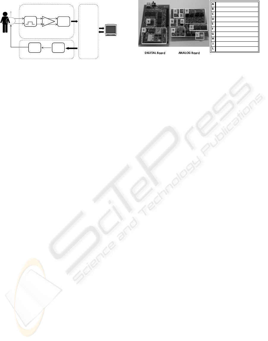
BPF
Amplifier
ADC
Digital System
Controller
for Data and Powering
Stimulation Circuitry
Recording
Circuitry
Electrodes
D
A
C
V/I
converter
Figure 1: Block diagram of the recording and stimulation
system.
unit. A programmable amplification stage is required
in order to exploit the full scale range of the ADC.
The architecture of the recording unit provides a fully
differential path for the signal so as to maximize the
common mode rejection and reduce the effect of in-
terferences.
Stimulation Unit: In the stimulation circuitry nerve
afferent activities towards the electrode are generated
by the digital system controller and converted first
into an analog voltage through the DAC then, into
a stimulation current signal by means of a V/I con-
verter. The function electrical stimulation (FES) sig-
nal can be software programmable in amplitude, fre-
quency and shape.
Digital Unit: The digital system controller has two
main tasks. First, it provides power from a recharge-
able battery to ensure the isolation of the patient from
the electric grid (both for safety reasons and to re-
duce the noise injected by the grid). Main task of the
module, however, is managing the configuration of
the whole system with the generation of timing sig-
nals (for multiplexers, ADC, DAC), programmable
gain and stimulation patterns. For a high-speed real
time data transmission and control, two different units
were integrated in the system: a Universal Serial Bus
(USB) controller and a wireless IEEE 802.11 module.
2.2 Working Modes
The implemented system works on three independent
modes: Recording, Stimulation and Testing mode.
This high degree of reconfigurability is guaranteed
thanks to the presence of a network of switches driven
by three digital signals. In Recording mode, the neu-
ral signal is captured from the tfLIFE electrode and is
sent to the recording circuitry. The signal is filtered,
amplified and digitally converted before being trans-
mitted to the digital system controller through SPI
communication. When the system is in Stimulation
mode, different digital patterns are generated by sys-
tem controller and converted into an analog voltage
by a DAC.
USB and Wi
Digital Signal Controller
DAC
Attenuation Circuitry
Band-
Pass Filter
Programmable Amplifier
ADC
Stimulation Circuitry
Analog Multiplexers
tf-
LIFE electrodes
USB and Wi
-Fi Controllers
Digital Signal Controller
DAC
Attenuation Circuitry
Pass Filter
Programmable Amplifier
ADC
Stimulation Circuitry
Analog Multiplexers
LIFE electrodes
Figure 2: Photograph of the implemented PCB system.
When the system is reconfigured for testing purposes,
the digital controller generates a test pattern that emu-
lates neural inputs and sends it to the DAC. Since the
converter output voltage swings from 0V to 3V , with
a resolution of 45.7µV , in order to manage and gen-
erate neural signals in the range of few microvolts, a
programmable attenuation circuit has been introduced
in the system.
3 CIRCUIT DESCRIPTION
Commercially available devices were adopted to build
up the interface and to validate the function of the cir-
cuits design. The main benefits of this solution are
highly reproducible, simple portable and low cost.
The fabricated prototype is shown in Fig. 2. Spe-
cial attention has been paid on how to isolate the
analog module from the interferences (especially on
supplies) generated by the digital unit. For this rea-
son the system has been divided into analog and dig-
ital parts and implemented in two separate, sandwich
stackable, printed circuit boards (PCB), sizing respec-
tively 7 cm x 6.1 cm and 7.5 cm x 5.8 cm. The cho-
sen solution could be suitable for a future fully im-
plantable version of the interface. The whole system
is supplied by a rechargeable battery (3.7V) to en-
sure the isolation of the patient from the electric grid.
Lower supply voltages (3V and 1.5V) are provided by
two linear voltage regulators (Maxim, MAX1589 and
MAX1792).
3.1 Neural Recording Circuit
Since neural recordings from tfLIFEs appear like
spikes with peak-to-peak amplitudes of about 50µV
and frequency band in range from 900Hz to 2kHz, it
is mandatory to eliminate DC components (50Hz) as
well as EMG and biological unwanted components.
Fortunately, these interferences are band-limited be-
low 300Hz and can be separated from the neural sig-
nal through an appropriate band-pass filtering inside
the frequency band of interest. For this reason, a se-
BIODEVICES 2010 - International Conference on Biomedical Electronics and Devices
212
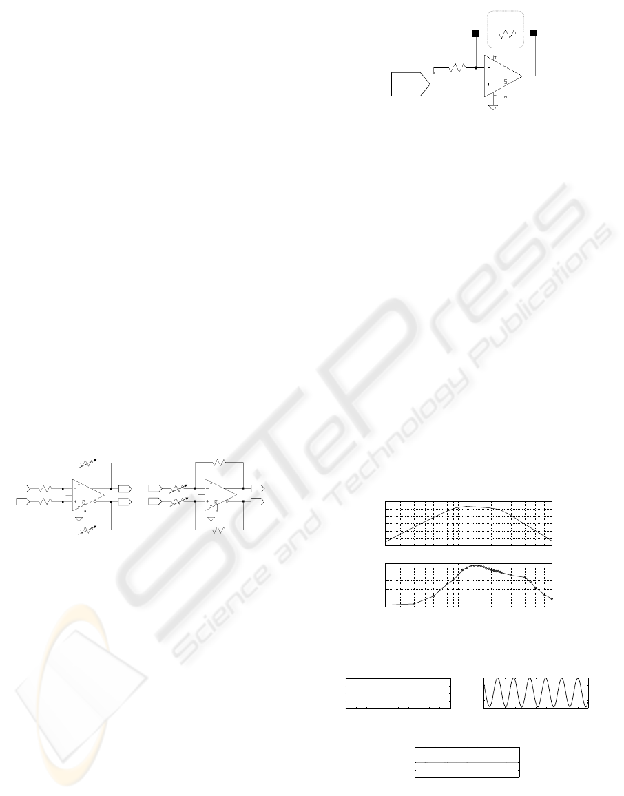
lective filter was integrated in the registration unit. It
is made up of a 4th order high-pass filter, cascaded
with a 4th order low-pass filter. The basic filter cell
has been implemented with Multiple Feedback topol-
ogy, using a very low noise density (3nV /
√
Hz) and
fully differential input/output amplifier (Linear Tech-
nology, LT1994). The filter design specification re-
quired a gain of 32dB and a frequency band between
900Hz and 2.3kHz. The RC filter network was sized
to reduce the input-referred noise (IRN) to 250nV in
the band of interest. Once that the signal has been
filtered, it can be further amplified through a pro-
grammable gain amplifier before being digitized. In
Fig.3(a) the chosen amplification circuitry is shown.
A digitally controlled potentiometer (R7) (Intersil,
ISL90727), in pair with a resistor of 100Ω (R6), al-
lows to obtain a gain factor between 1 and 100, for
a total of 127 different values. Note that, using R6
as potentiometer and R7 with a fixed value of 100Ω,
it has been possible to use the same circuitry to ob-
tain the programmable attenuation circuit of Fig.3(b)
useful during the test operating mode. Finally, the
recording system includes an analog-digital converter
(Analog Devices, AD7687) with a resolution of 16-
bit and a power consumption of 1.3mW , that by SPI
communication provides to the digital control unit the
processed signal.
ISL90727
Vp
Vm
R6
R6
R7
vdd
vcm
LT1994
V
outm
V
outp
ISL90727
R7
ISL90727
(a) Amplification cir-
cuitry
Vp
Vm
R6
R6
R7
R7
vdd
vcm
LT1994
V
outm
V
outp
ISL90727
ISL90727
(b) Attenuation cir-
cuitry
Figure 3: Circuitry used for amplification and attenuation.
3.2 Neural Stimulation Circuit
Key role for the application is played by the neu-
ral stimulation circuit. The stimulation is done with
current patterns that have programmable amplitude,
frequency and shape. Fig. 4 shows the architec-
ture of the stimulation unit. The circuit was imple-
mented using a 16-bit D/A converter (Linear Tech-
nology, LTC2641) followed by a V/I converter (Texas
Instruments, OPA343). The basic idea is to con-
vert a programmable voltage, generated by the DAC,
into a stimulation current that will flow through the
electrodes. Note that resistor Relectr represents the
impedance between the measurement (L1 −L4, R1 −
R4) and reference (L0 −R0) electrode.
DAC
Rstim
tfLIFE
vdd
OPA343
LTC2641
Relectr
L0,R0
Li,Ri
Figure 4: Neural stimulation circuitry.
3.3 Digital System Controller
Two high-performance Microchip Microcontrollers
have been used for the bi-directional communication
PC ⇐⇒ AnalogBoard: the dsPIC33Fj256GP506 and
the PIC18LF4550. The first one allows to manage
the ADC and DAC modules by means of a SPI bus
and to choose the value of the digitally potentiometers
through an I
2
C bus. While the PIC18LF4550 is used
as USB controller in the communication PC −dsPIC,
providing a communication speed of 64KB/s per re-
port, according to the specific class of HID (Human
Interface Devices).
4 EXPERIMENTAL RESULTS
In order to characterize the filter, sinusoidal signals at
different frequencies have been generated by the DAC
and applied to the filtering circuitry for testing.
10
3
−20
−10
0
10
20
30
40
Frequency (Hz)
Magnitude (dB)
Simulated BPF Frequency Response
10
3
0
5
10
15
20
25
Frequency (Hz)
Magnitude (dB)
Measured BPF Frequency Response
Figure 5: Plot of theoretical and measured frequency re-
sponse of the band-pass filter.
0 0.5 1 1.5 2 2.5 3 3.5 4 4.5 5
−0.2
−0.1
0
0.1
0.2
Time (ms)
Amplitude (V)
(a) Signal at 400 Hz
0 0.5 1 1.5 2 2.5 3 3.5 4 4.5 5
−0.2
−0.1
0
0.1
0.2
Time (ms)
Amplitude (V)
(b) Signal at 1.3 kHz
0 0.5 1 1.5 2 2.5 3 3.5 4 4.5 5
−0.2
−0.1
0
0.1
0.2
Time (ms)
Amplitude (V)
(c) Signal at 5kHz
Figure 6: Band pass filter output signal.
The frequency response of bandpass filter is shown
in Fig. 5. The graphic above shows the simulations
AN ELECTRONIC INTERFACE FOR NEURAL ACTIVITY RECORDING AND STIMULATION
213
results, while the lower panel shows the frequency re-
sponse obtained by the filter test. As shown in the
first panel, the designed filter has a gain equal to 32dB
in bandwidth (900Hz −2.3kHz) while at 400Hz and
6kHz the attenuation of the signal is over 20dB. The
results of measurements show a lower gain (24dB)
and a band between 1.1kHz and 2kHz. The deviations
from the ideal behavior are due to manufacturing tol-
erances of the resistances and capacities used in the
feedback network of the filter. The selectivity of the
band-pass filter has been tested using as input for the
recording circuitry a sinusoidal signal at different fre-
quencies: 400Hz, 1.3kHz and 5kHz. The effect of the
band-pass filtering is evident in Fig. 6(b), where the
sine at 1.3kHz is allowed to pass. The signals shown
in Fig. 6(a) and in Fig. 6(c), prove how out-band fre-
quencies are completely filtered.
1520 1522 1524 1526 1528 1530
1.4
1.6
1.8
2
Time (s)
Amplitude (V)
(a) Input Signal
1520 1522 1524 1526 1528 1530
−0.8
−0.4
0
0.4
0.8
Time (s)
Amplitude (V)
(b) Matlab Filtered Signal
1520 1522 1524 1526 1528 1530
−0.8
−0.4
0
0.4
0.8
Time (s)
Amplitude (V)
(c) PCB Filtered Signal
Figure 7: Neural signal processing: filtering, amplification
and digital conversion.
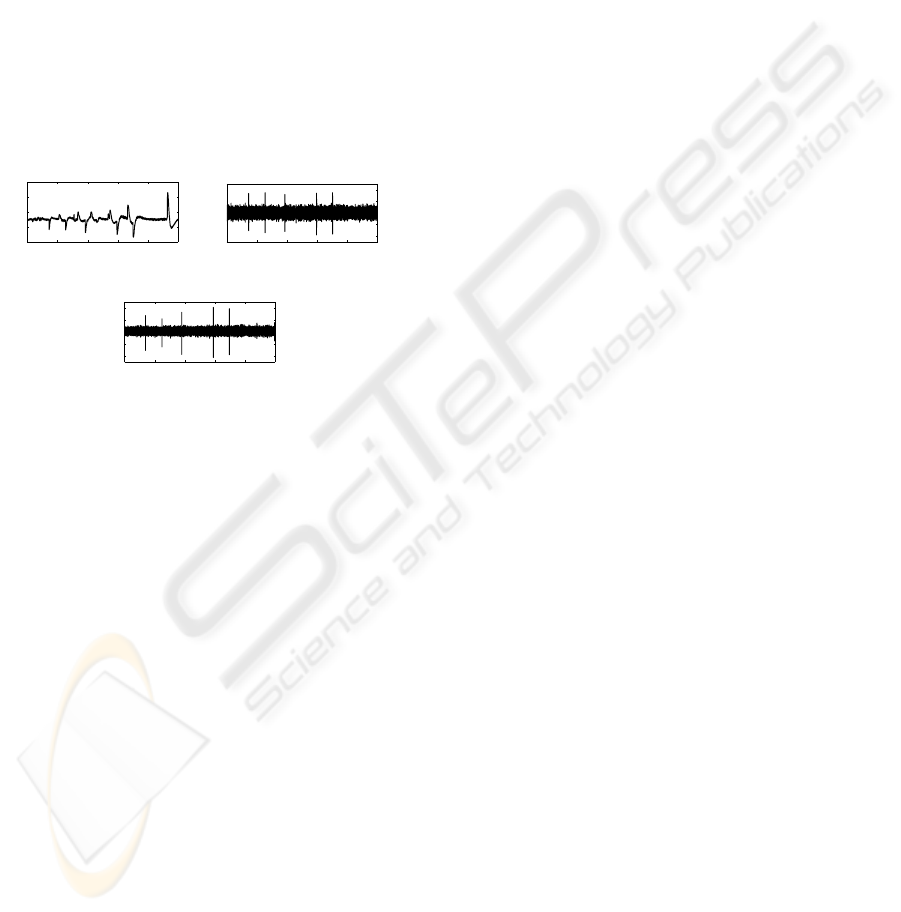
Finally, the whole recording system has been tested in
its functionalities using stimuli supplied by the Scuola
Superiore di on the basis of recordings made in clini-
cal trials with rabbits. The input pattern represented in
Fig. 7(a) is the result of ten recording seconds during
which the rabbit was subjected to vibrations at 50Hz
and 100Hz in cutaneous afferents.
In a first phase of simulation, the available input
pattern of Fig. 7(a) has been processed with Matlab
using an ideal band-pass filter. In Fig. 7(b) the ideal
filtered signal obtained is shown. The heavy influ-
ence of low-frequencies noise has been deleted and
is clear the presence of the useful signal components
that in the input pattern were completely masked. The
filtered signal obtained with the implemented neural
recording circuitry, is represented in Fig. 7(c). The
slow components of the input signal coincide with
output peaks characterized by higher frequencies.
5 CONCLUSIONS
We have developed and tested a PCB system for neu-
ral activity recording and stimulation. Given the na-
ture of the signals to be acquired, special design tech-
niques for low noise and low power consumption have
been adopted. The first experimental results prove
that the system works correctly and stably, with the
possibility to acquire and process neural signal in mi-
crovolts order. The recording circuitry allows to filter
the neural signals in the band of 1kHz −2.2kHz, pro-
viding a programmable gain that covers values from
24dB to 44dB. The resulting signal can be digi-
tally converted and sent to PC for further processing
through USB or Wi-Fi transmission. The acquisition
system has been tested using pre-recorded neural pat-
terns extracted by rabbit with tfLIFE electrodes. The
system has been studied in order to generate also elec-
trical stimuli with controlled current amplitude, du-
ration and shape. This effort is part of an on-going
research program which aims to develop smart im-
plantable devices dedicated to neural activity record-
ing and stimulation.
REFERENCES
Gosselin, B. and Sawan, M. (2005). A low power portable
multichannel neural data acquisition system. Proceed-
ings of 10th Annual Conference of the International
FES Society, pages 391–393.
Jochum, T., Denison, T., and Wolf, P. (2009). Integrated cir-
cuit amplifiers for multi-electrode intracortical record-
ing. J. Neural Eng., 6.
Obeid, I., Nicolelis, M., and Wolf, P. (2004). A low power
multichannel analog front end for portable neural sig-
nal recordings. J. Neurosci. Meth., 133:27–32.
Salzman, C. D. and Newsome, W. T. (1994). Neural mech-
anisms for forming a perceptual decision. Science,
264:231–237.
Wang, Y., Wang, Z., L, X., and Wang, H. (2005). Fully
integrated and low power cmos amplifier for neural
signal recording. IEEE Engineering in Medicine and
Biology Society, pages 5250–5230.
Watkins, P., Kier, R., Lovejoy, R., Black, D., and Harrison,
R. (2006). Signal amplification, detection and trans-
mission in a wireless 100-electrode neural recording
system. pages 2193–2196.
Wessberg, Stambaugh, C., Kralik, J., Beck, P., Laubach,
M., Chapin, J., Kim, J., Biggs, S., Srinivasan, M., and
Nicolelis, M. (2000). Real-time prediction of hand
trajectory by ensembles of cortical neurons in primate.
Nature, 408(68102):361–365.
Yoshida, K., Hennings, K., and Kammer, S. (2006).
Acute performance of the thin-film longitudinal intra-
fascicular electrode. IEEE Conference Biomedical
Robotics and Biomechatronics, BioRob, pages 296–
300.
BIODEVICES 2010 - International Conference on Biomedical Electronics and Devices
214
