
AL
2
O
3
NANOLAYER AS EVANESCENT WAVEGUIDE
FOR BIOMEDICAL SENSOR APPLICATION
A. Purniawan, P. J. French
Electronic Instrumentation Laboratory (EI), TU Delft, Mekelweg 4, room 13.260, 2628 CD Delft, The Netherlands
Y. Huang
,
G. Pandraud, P. M. Sarro
Delft Institute of Microsystems and Nanoelectronics (DIMES), TU Delft
Feldmannweg 17, 2628 CT Delft, PO Box 5053, 2600 GB Delft, The Netherlands
Keywords: Evanescent waveguide, Drain fluid, Anastomosis leakage, ALD, Thin film stress.
Abstract: The aim of our research is to develop a sensitive sensor for biomedical applications. A nanolayer Al
2
O
3
is
used as evanescent waveguide. The material was deposited on a silicon wafer by using atomic layer
deposition (ALD). In the present paper, we will report the preliminary results of our project such as
deposition, characterization of nanolayer, and evanescent waveguide sensor design. Lambert beer’s law and
some waveguide concepts are combined in the design to obtain the optimum parameters of the evanescent
waveguide sensor. Furthermore, characterizations to investigate optical properties and internal stress of the
thin film were done. Based on the results of lattice parameter analysis, we can conclude that thin film
thickness have effect not only on sensitivity of the sensor but also on the mismatch stress between substrate
and thin film. Design results show that a thickness of waveguide of 50 nm and an optical path length of the
sensor of 1 mm can be used as waveguide dimension with a transmission of 75%. 50 nm thin film thickness
shows low mismatch stress and that was shown by high radius curvature 32.34 m.
1 INTRODUCTION
Anastomosis is an operation to make continue the
organ as like colon, bowel, pancreas etc.
Anastomosis leakage is still a problem in medical
especially post-operate. The patient’s mortality rate
due to anastomosis leakage is still high, because
often the leakage is identified too late. The
indication of anastomosis leakage is the presence of
a high concentration of bacteria in the drain fluid.
There are many types of bacteria like Bacteriodes
sp., Lactobacillus acidophilus, Klebsiella sp., and
Eschericia coli (E. Coli) in drain fluid. These
bacteria are essential for food digesting. However,
due to malfunction in the colon, bacteria could enter
the abdominal cavity causing severe infections
(Chaeron, 2007 and Pakula et al., 2005).
The conventional identification needs at least
seven days to obtain accurate results. Currently,
there are three existing experiment methods to
perform a microbiological analysis on drain fluid,
being bacteria culture, Raman spectroscopy, and
polymerase chain reaction (PCR) to make million
DNA copies of the bacteria. The disadvantages of
the methods are the time to analyze and high cost.
In our research, an evanescent waveguide
sensor is developed to detect bacteria in drain fluid
as an indication of anastomosis leakage. The
properties of material and structure are very
important to obtain a sensor with high sensitivity.
Aluminum oxide (Al
2
O
3
) has a high refractive index.
Therefore the material has high potential as thin film
material waveguide. Atomic layer deposition (ALD)
was used to deposit Al
2
O
3
due to its advantages to
produce high conformality, uniformity, and
smoothness. In order to obtain optimal parameters,
Lambert beer’s law and waveguide evanescent
sensors were combined to calculate the optimal
waveguide dimensions. In this paper, we present
evanescent waveguide sensor design and
experimental results of the optical and structural
characterization.
1.1 Lambert Beer’s Law
Lambert beer’s law is often used to analyze the
44
Purniawan A., French P., Huang Y., Pandraud G. and Sarro P. (2010).
AL2O3 NANOLAYER AS EVANESCENT WAVEGUIDE FOR BIOMEDICAL SENSOR APPLICATION.
In Proceedings of the Third International Conference on Biomedical Electronics and Devices, pages 44-48
DOI: 10.5220/0002751400440048
Copyright
c
SciTePress

absorbance (A) of media while light is transmitted in
the media. The transmission of light is called
transmissivity (T), the ratio between output and
input of light. The transmissivity is expressed as:
o
I
T
I
=
(1)
And the formula of absorbance as:
A
cl
σ
= (2)
The relationship between transmission and
absorbance is as follows:
10 10
1
log 2 log %
A
T
T
==−
(3)
Where σ is the molar absorption coefficient (M
-1
cm
-
1
), c is media concentration and l is path length of
light in waveguide (cm).
1.2 Evanescent Waveguide Design
Planar waveguide is more used in optical integrated
system. The source of light couples with edge of
waveguide and the receiver in the other side. The
light through the waveguide with difference
refractive index between core and cladding such as
n
1
is refractive index of core (Al
2
O
3
) and n
2
is
refractive index of cladding. Furthermore, the light
wave through the optic material with angle (
θ
1
) is
called incident angle and the reflective angle (
θ
2
) is
the angle of the direction of the reflection light
wave. In order to obtain maximum reflection, the
expected light way in the cladding is at lease parallel
with the both materials interface and other word that
the reflective angle (
θ
2
) is 90
o
. The critical incidence
angle is defined as the minimum incident angle to
obtain a reflective angle of 90
o
.
By using Snell’s law,
the critical incidence angle can be calculated.
Critical incidence angle implies
θ
2
= 90
o
and that
sin
θ
2
= 1. Hence, the critical incident angle can be
expressed as:
1
2
1
1
sin
n
n
θ
−
⎛⎞
=
⎜⎟
⎝⎠
(4)
In the evanescent sensor wave guide, penetration
depth is the maximum depth from which the sensor
can obtain information. The penetration depth is
very important to estimate the performance of sensor
to detect objects in the sensor surroundings. The
range over which excitation is possible is limited by
the exponential decay of the evanescent wave energy
in the z-direction, perpendicular to the interface. In
this case energy is proportional with light intensity.
The following equation defines this intensity as a
function of distance from the interface:
()
exp
z
d
zo
II
−
=
(5)
I
z
is the energy at a perpendicular distance z from the
interface, and I
0
is the energy at the interface. The
penetration depth state when d = z and the
penetration depth intensity is 100% x e
-1
(36.7% I
o
).
The range over which excitation is possible is
limited by the exponential decay of the evanescent
wave energy in the z-direction. The penetration
depth d, is dependent upon the wavelength of the
incident illumination, λ
i
, the angle of incidence, and
the refractive indices of the media at the interface,
according to the Equation (6) and the general
formula of light propagation in waveguide expressed
in Equation (7).
()
1
22 2
2
112
sin
4
i
dxn n
λ
θ
π
−
=−
(6)
2
1
12
2
12
2
22
22
22
2
22
22
2
arctan
arctan 0
eff eff
eff
eff
eff eff
eff
p
p
nnn
t
nn
nn n
nnn
m
nn n
π
λ
π
⎡
⎤
⎛⎞
−
⎢
⎥
+−
⎜⎟
⎜⎟
−
⎢
⎥
⎝⎠
⎣
⎦
⎡⎤
⎛⎞
−
⎢⎥
−−=
⎜⎟
⎜⎟
−
⎢⎥
⎝⎠
⎣⎦
(7)
Where n
eff
is refractive index effective and m is
constant of waveguide mode.
1
.sin
eff
nn
k
β
θ
==
(8)
Where
β
is the propagation constants along z is
expressed by
β
= k.n
1
sin
θ
. Furthermore the Eq. (7)
is derived to obtain the normalized parameters that
to be used to calculate geometry of the sensor that
the more detail was be explained by Veldhuis et al,
2000. Cutoff condition is the optimum condition
when the effective refractive index is equal to the
cladding’s refractive index. Then, the sensitivity of
sensor can be calculated using equation
22
2
2
2
2
1
eff eff
eff tot
nnn
P
S
nnP
⎧⎫
−
⎪⎪
=+
⎨⎬
⎪⎪
⎩⎭
(9)
Where S is sensitivity, P
c
/P
tot
is ratio energy
(intensity), n
2
is cladding’s refractive index.
2 EXPERIMENTAL
A silicon wafer was used as substrate material
whereas the Al
2
O
3
as thin film material. In order to
obtain homogeneity, conformality and low internal
stress, ALD was employed to deposit the thin film.
Tetra methyl aluminum (Al(CH
3
)
4
) and H
2
O are as
precursors and N
2
is used as gas carrier. The cycle
AL2O3 NANOLAYER AS EVANESCENT WAVEGUIDE FOR BIOMEDICAL SENSOR APPLICATION
45
processes used ratio 1:2:1:3 s. It means that the pulse
time is one second for 1
st
precursor (Al(CH
3
)
4
), two
seconds for purge (N
2
), then one second for 2
nd
precursor (H
2
O) and finally three seconds for purge
(N
2
). The total time for one cycle is seven seconds.
Process temperature is 300
o
C. Subsequently the thin
film was characterized using Atomic Force
Microscope (AFM) to investigate topography and
surface roughness of thin film, thickness
measurement and stress measurement to measure the
internal stress of thin film.
In the fabrication process, to pattern the
structure, three masks for contact aligner lithography
were designed consists of two masks for front side to
make ribs and bridges structures and one mask to
open SiO
2
in backside. Firstly, the process
fabrication makes windows in the backside. Then
after patterning the front side and finally etching the
backside. The structure is made the free standing.
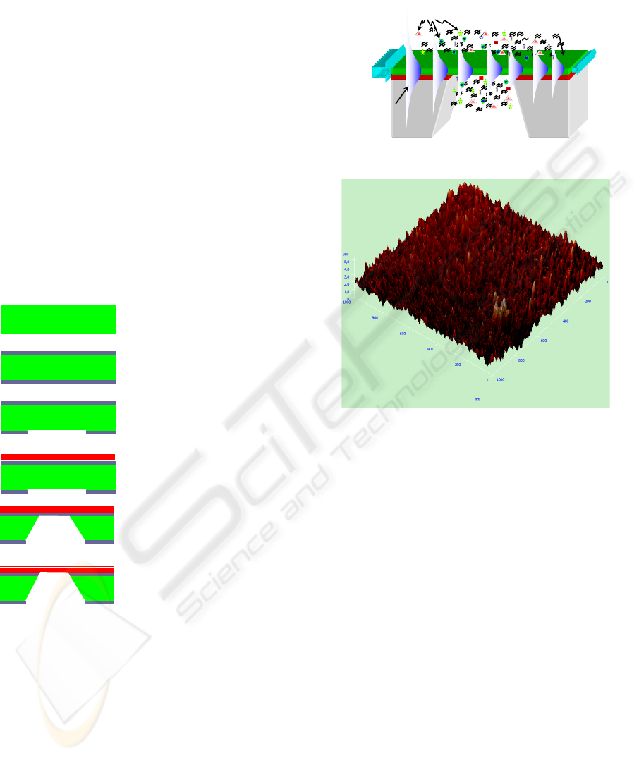
The flowchart of the detail process is shown in Fig.
1(a) – (f).
Figure 1: Fabrication process flowchart for waveguide free
standing structure
.
The freestanding waveguide structure and
evanescent field region is shown in Figure 2.
3 RESULTS AND DISCUSSIONS
Based on experiment results, the thickness of Al
2
O
3
is 46.6 nm during 500 cycles, (0.9Å/cycle), the
refractive index is 1.65 and the internal stress of
Al
2
O
3
thin film is 246 MPa. By using AFM, the
surface topography and surface roughness of Al
2
O
3
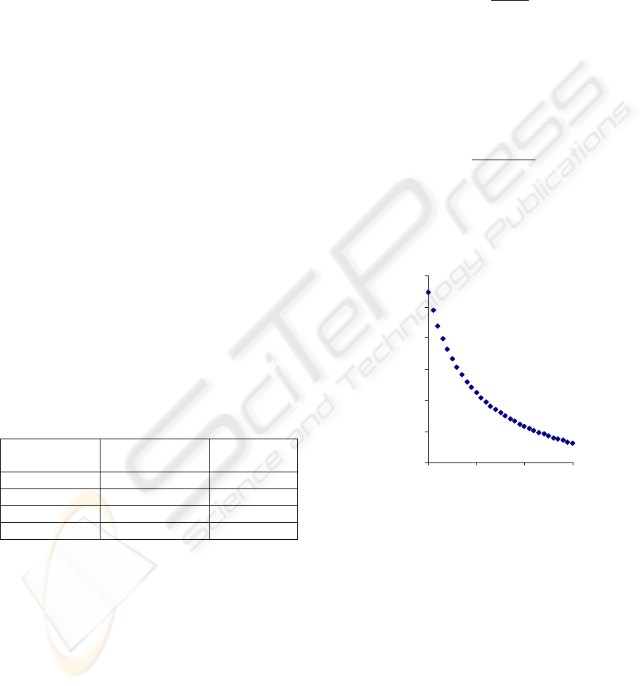
can be seen in Figure 3.
Figure 2: Evanescent waveguide.
Figure 3: AFM Topography of Al
2
O
3
-ALD with root mean
square 0.5 nm.
In previous research of our group, drain fluid
transmission analysis was conducted by using
visible light and infrared light wavelength. The
results show that the visible light spectrum did not
show any distinction wavelength at which the
transmission was implicitly bacteria contamination
dependent. Moreover, low contamination was not
measurable with the visible light set-up. The other
wavelength, infrared spectrum was used in the
experiment. Infrared wavelength spectrums 2µm and
4.3µm have high sensitivity to make difference
transmission results when the light through drain
fluid (Pakula et al, 2005). It means that both
wavelengths can be used as light source in drain
fluid analysis. In the present research 2 µm
wavelength is used as light input of the sensor. In
addition, drain fluid with variable bacteria
concentrations analysis to obtain the transmission
percentage was conducted in previous experiment by
our group (Chaeron, 2007).
From medical point of view, 20% concentration
of bacteria in drain fluid is the critical range. The
results from the experiment were taken for further
Drain fluid, n
2
Light
source
Si
Si
Bacteria
Output
Evanescent
field region
Drain fluid, n
2
Al
2
O
3
, n
1
(a) Starting material (N-type
100 Silicon wafer)
(b) 2 micron SiO
2
using wet
thermal oxidation for 8
hours 12 minutes
(c) Open SiO
2
windows in the
backside plasma etching
Drytec Triode for 6
minutes.
(d) 100nm Al
2
O
3
deposition
using ALD then patterning
rib and bridge on the front
side using RIE Alcatel
plasma etching
(f) SiO
2
backside etching
using RIE Alcatel.
(e) Backside etching using
TMAH with protecting
holder on the front side
(etching process stop on
SiO
2
)
BIODEVICES 2010 - International Conference on Biomedical Electronics and Devices
46
analysis, especially near critical concentration (20%)
which is 25% bacteria concentration. By taking
value of transmission of drain fluid with E.Coli exist
in the drain fluid for 1 day after taken from patient
and path optical length 0.865 cm, the transmission
result is 8.3% then the transmission value is plotted
in Figure 1 to obtain the absorbance value is 1.08.
By using Equation (2) can be calculated the molar
absorption coefficient which is 0.4998. Furthermore,
the optical path length is fixed at 1 mm and using the
Equation (2) the absorbance is 0.125. By plotting the
absorbance result to Figure 1, the transmission value
is found to be 75%.
The important parameters have to be analyzed
to obtain the critical incident angle. It depends on
material properties especially refractive index of the
materials of both core and cladding material. The
incident angle must be more than critical angle to
obtain total reflection. Based on measurement Al
2
O
3
,
deposited by ALD, refractive index ‘n
1
’
is 1.646.
Cladding’s refractive index ‘n
2
’ is 1.33. The angle
can be calculated from Snell’s law modified as
Equation (4) and the result of critical incident angle
is 53.9
o
. In this experiment, the waveguide will be
coupled with source of light with incident angle 90
o
,
λ
i
= 2000 nm and using Equation (6), the penetration
depth of the waveguide sensor can be calculated of
164 nm. Due to the symmetrical waveguide, a
maximum sensitivity S
max
= 2.S (Velduis et al, 200).
Hence, using Equation (9) can be found the
maximum sensitivity of sensor as shown in Table 1.
Table 1: Sensitivity of waveguide of varying waveguide
thickness.
Thickness, nm
(t)
Effective index
(n
e
ff
)
Sensitivity
(S
max
)
50 1.331 0.997
100 1.333 0.989
150 1.338 0.975
200 1.344 0.965
The film has as incompatible elastic mismatch
strain with respect to the substrate; this strain might
be due to thermal expansion effects, epitaxial
mismatch, phase transformation, chemical reaction,
moisture absorption or other physical effects.
Whatever the origin of the strain, the goal here is to
estimate the curvature of the substrate, within the
range of elastic response, induced by the stress
associated with the incompatible strain.
Stoney’s formula is original analysis of the
stress in a thin film deposited on a rectangular
substrate was based on a uniaxial state of the stress.
Consequently, his expression for curvature did not
involve use of the substrate biaxial modulus M
s
.
Consequently, it can be applied in situations in
which mismatch derives from in elastic effect (Freud
and Suresh, 2003). The expression for curvature is
famous Stoney’s formula relating curvature to stress
in the film as:
2
6
mf
s
s
h
M
h
σ
κ
=
(10)
Where
κ
represents the curvature, or inverse of the
radius of curvature, of this plane,
σ
f
is mean stress,
h
f
is the thickness of the thin film, M
s
is substrate
biaxial modulus and h
s
is substrate thickness. The
mean mismatch strain of substrate and the
corresponding mismatch stress of thin film
expressed as:
23
23
Si Al O
m
Al O
aa
a
ε
−
=
(11)
mmf
M
σε
=
(12)
Figure 4 shows the curvature radius of various thin
film thickness. The curvature radii gradually
decrease with increasing thin film thickness.
5
10
15
20
25
30
35
50 100 150 200
Thickness
(nm)
Radius (m)
Figure 4: Curvature radius as function of thin film stress of
Al
2
O
3
in the surface substrate with various thin film
thickness.
By taking the thin film thickness h
f
= 50 nm of Al
2
O
3
is grown on Si-wafer substrate with thickness h
s
=
500 µm, lattice parameter of a
Al
= 0.405nm, a
O
=
0.683 nm and a
Si
= 0.5431nm. The lattice parameter
of Al
2
O
3
at room temperature is a
Al2O3
= 0.53a
Al
+
0.47a
O
= 0.536 nm. The biaxial modulus of Al
2
O
3
(M
f
) and Si (M
s
) are 380 GPa and 180.5 GPa,
respectively. By substitute Equation (11) and
Equation (12) into Equation (10) can be obtained
κ
=
0.031. Then the change of curvature radius is
ρ
=
κ
-1
= 32.34 m. The result of the curvature value is
AL2O3 NANOLAYER AS EVANESCENT WAVEGUIDE FOR BIOMEDICAL SENSOR APPLICATION
47

positive (+), it implies that the substrate is convex on
the face away from the bonded film.
4 CONCLUSIONS
The optimum condition of evanescent wave guide
sensor for anastomosis leakage detection can be
estimated by analytical and then should be verified
by experiments. In the preliminary results, we found
that AL
2
O
3
deposited on Si-wafer have high
potential as waveguide sensor. Based on the results,
it can be concluded that thin film thickness have
high effect not only on sensitivity of the sensor, but
also on the mismatch stress between substrate and
thin film. That was shown by high radius curvature
32.34 m with convex structure for thickness 50nm.
ACKNOWLEDGEMENTS
The authors would like to acknowledge the Dutch
Technical Foundation, STW and the support
provided by Electronic Instrumentation Laboratory
(EI) and The Delft Institute of Microsystems and
Nanoelectronics (DIMES), TU Delft, The
Netherlands. The authors also wish to thank IC
process group of DIMES for technical assistance.
REFERENCES
Chaeron, S. R. A. (2007) "An optical measurement system
for the analysis of bacteria in drain fluid," MSc Thesis,
TUDelft, The Netherlands.
Pakula, M. P, D. Tanase, K. Kraal, G. d. Graaf, J. F.
Lange, and P. J. French, (2005), "Optical
Measurements on drain fluid for the detection of
anastomotic leakage," Proceedings of the 3rd Annual
International IEEE EMBS Special Topic Conference
on Microtechnologies in Medicine and Biology,
Kahuku, Oahu, Hawaii pp. 72 - 75.
Veldhuis, G. J., O. Parriaux, H. J. W. M. Hoekstra, and P.
V. Lambeck, (2000), "Sensitivity Enhancement in
Evanescent Optical Waveguide Sensors," J. Lightwave
Technol., vol. 18, pp. 677.
Freund L. B, and S. Suresh, (2003), The book, "Thin Film
Materials: Stress, Defect Formation and Surface
Evolution," Cambridge University Press.
BIODEVICES 2010 - International Conference on Biomedical Electronics and Devices
48
