
ELECTRICAL RELIABILITY OF Cu/Sn MICRO-BUMP IN
WAFER LEVEL PACKAGING FOR BioMEMS DEVICES
Myeong-Hyeok Jeong, Jae-Won Kim, Byung-Hyun Kwak, Young-Bae Park
School of Materials Science & Engineering, Andong National University, Andong, 760-749, Korea
Byoung-Joon Kim, Young-Chang Joo
Department of Materials Science & Engineering, Seoul National University, Seoul, 151-744, Korea
Keywords: Cu/Sn micro-bump, Electromigration, Wafer Level Packaging, BioMEMS Devices.
Abstract: The electrical reliability of Cu/Sn micro-bump in wafer level packaging for advanced BioMEMS devices
applications were systematically investigated during current stressing condition. After bump bonding,
Cu
3
Sn
and
Cu
6
Sn
5
intermetallic phases were observed, and Cu
3
Sn formed and grew at Cu pillar/Cu
6
Sn
5
interface with increasing annealing and current stressing time. The kinetics of intermetallic compound
growth changed when all Sn in Cu/Sn micro-bump was exhausted. The complete consumption time of Sn
phase in electromigration condition was faster than that in annealing condition. Under current stressing
condition, intermetallic compound growth was significantly enhanced by current stressing where the growth
rate follows a linear relationship with stressing time.
1 INTRODUCTION
Through-Si-via technology using flip-chip solder
bump has recently been investigated in high
performance wafer level packaging for advanced
BioMEMS device packaging (Chiang, Lee, Lee, and
Chen, 2006). This technology assists in the
achievement of high performance and
miniaturization because the chip and the substrate
are directly connected to solder bumps. As the
integration of devices increased, the size of solder
bump in wafer level packaging became smaller with
fine pitch. And increase of current density due to
miniaturization of solder bump size with fine pitch
causes serious reliability issues of wafer level
packaging for advanced BioMEMS applications.
The solder bumps become spherical to minimize the
surface energy during reflow process (Rao, Tay,
Kripseph, Lim, and Yoon, 2004). Bump bridging is
caused by the shape of solder in miniaturized
electronics. It is limited to applications with a fine
pitch below 100 um. Therefore, a new shape for the
bump structure is necessary to address this limitation.
Cu/Sn micro-bumps are known to be one of the most
promising candidates for the fine pitch
interconnection materials in wafer level packaging
because they do not cause bump bridging between
adjacent bumps and uniform current distribution
(Son, Jung, Park, and Paik, 2008). Electrical
reliability issues can also be solved with this
structure because Cu pillars have superior electric
conductivity. At the interface between Cu and solder,
Cu6Sn5 and Cu3Sn are formed by the reaction of Cu
and Sn, and Kirkendall void is grown (Tu, Mayer,
Feldman, 1992). Additionally, the high
concentration of Sn in Pb-free solder induces more
excessive growth of intermetallic compounds
(IMCs) than eutectic SnPb solder (Lee, Zhang,
Wong, Tan, and Hadikusuma, 2006). IMCs growth
and Kirkendall void formation are important
reliability issues of wafer level packaging for
advanced BioMEMS devices because IMCs is brittle
and has higher resistivity than solder or Cu, which
results from the difference in the intrinsic
diffusivities of Cu and Sn, in solder joints severely
deteriorate the mechanical strength of the joints. The
mechanical reliability of solder joints is sensitive to
the solder reaction and the microstructure of the
solder. Therefore, to ensure the bonding reliability of
wafer level packaging for advanced BioMEMS
devices, a deep understanding of the IMC growth
between Cu and solder is necessary. Many
researchers have studied IMCs formation and the
growth between Cu and solder in solder bumps and
thin film structures (Chao, Chae, Zhang, Lu, Im, and
Ho, 2007); but the IMCs growth behaviours in
311
Jeong M., Kim J., Kwak B., Park Y., Kim B. and Joo Y..
ELECTRICAL RELIABILITY OF Cu/Sn MICRO-BUMP IN WAFER LEVEL PACKAGING FOR BioMEMS DEVICES.
DOI: 10.5220/0003122603110314
In Proceedings of the International Conference on Biomedical Electronics and Devices (BIODEVICES-2011), pages 311-314
ISBN: 978-989-8425-37-9
Copyright
c
2011 SCITEPRESS (Science and Technology Publications, Lda.)
Cu/Sn micro-bumps have not been studied
systematically. Moreover, under electric current
stressing, the IMCs growth is accelerated by the
influence of by the electron wind force (Tu, Mayer,
and Feldman, 1992, Lee, Zhang, Wong, Tan, and
Hadikusuma, 2006, Chao, Chae, Zhang, Lu, Im, and
Ho, 2007). Because the current density of Cu/Sn
micro-bump is high due to its small size, it is
important to understand this behaviour. In this paper,
the IMCs growth behaviours in Cu/Sn micro-bumps
during simple annealing and under current stress
condition was studied systematically using in-situ
scanning electron microscope (SEM) observations.
IMC growth behaviour of the same sample could be
observed in detail by in-situ method which enables
us to observe IMCs growth as a function of time in
Cu/Sn micro-bumps.
2 EXPERIMENT
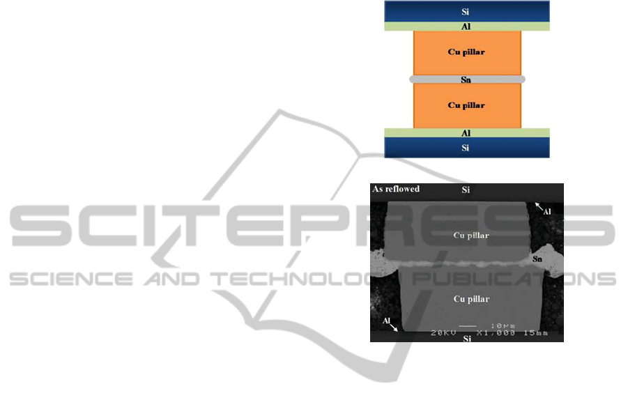
The schematic and SEM image of the Cu/Sn micro-
bump were shown in Fig. 1. The pad on the Si chip
was sputtered with a 2-μm-thick Al film. An Al line
provided the electrical path on the Si chip side. A Cu
pillar and pure Sn were formed with thicknesses of
40 μm and 1 μm, respectively, on the Al pad using
an electroplating process. The thickness and
diameter of the Cu/Sn micro-bump were 40 μm and
80 μm, respectively. Pure Sn solders at both the chip
and chip were directly interconnected during the
bonding process. The bonding was followed by a
reflow process with the peak reflow temperature
fixed at 280℃. The bonding time and load were 7 s
and 35 N, respectively. Just after bonding, all
samples have similar Sn thicknesses between 1.5 μm
and 2 μm. The samples were cross-sectioned with
sandpaper after the reflow. To investigate the
interfacial microstructure evolution and IMC growth
in Cu/Sn micro-bump, in-situ annealing tests were
performed via SEM at temperatures of 125℃. And,
electromigration test from effect of temperature
during current stressing were performed condition
with current density of 3.6×10
4
A/cm
2
at 125℃. The
temperature of the sample was kept at 125℃ by
attaching thermo-couple on Si chip. IMC growth
was observed at every 20~40 hours. IMC growths at
applying various current densities were observed by
in-situ as well. The evolution of each interfacial
microstructure and the IMC growth of Cu/Sn micro-
bumps were analyzed using SEM in back-scattered
electron (BSE) mode and energy-dispersive x-ray
spectroscopy (EDS). IMC thickness was measured
from the IMC layers at both the chip and substrate
sides. The Cu-Sn IMC thickness was quantified with
an image analyzer where the IMC thickness was
defined by dividing the area of the IMC by the
interface length.
(a)
(b)
Figure 1: (a) Schematic diagram and (b) SEM image of
Cu/Sn micro-bump structure.
3 RESULTS AND DISCUSSION
3.1 Interfacial Reaction Characteristics
during Annealing
To observe the evolution of the interfacial
microstructure and the growth of Cu-Sn IMCs on
Cu/Sn micro-bumps with annealing temperature and
time, BSE images were taken of cross-sectioned
Cu/Sn micro-bump annealed at 125℃, as shown in
Fig. 2. The SEM and EDS results suggest that only
Cu
6
Sn
5
was observed at the Cu pillar/Sn interfaces,
and micro-voids exist in the Sn phase after reflow.
The micro-voids seem to originate from the flip-chip
bonding process, and they arise from the defects in
the samples. Kirkendall voids were observed at the
Cu pillar/Cu
3
Sn interface as well as within the
Cu
3
Sn layer. It has been reported that the Kirkendall
void formation mechanism is ascribed to the
different diffusivities of Cu and Sn (Tu, Mayer, and
Feldman, 1992).
Cu
3
Sn formed and grew at the Cu
pillar/Cu
6
Sn
5
interface with increasing annealing
BIODEVICES 2011 - International Conference on Biomedical Electronics and Devices
312
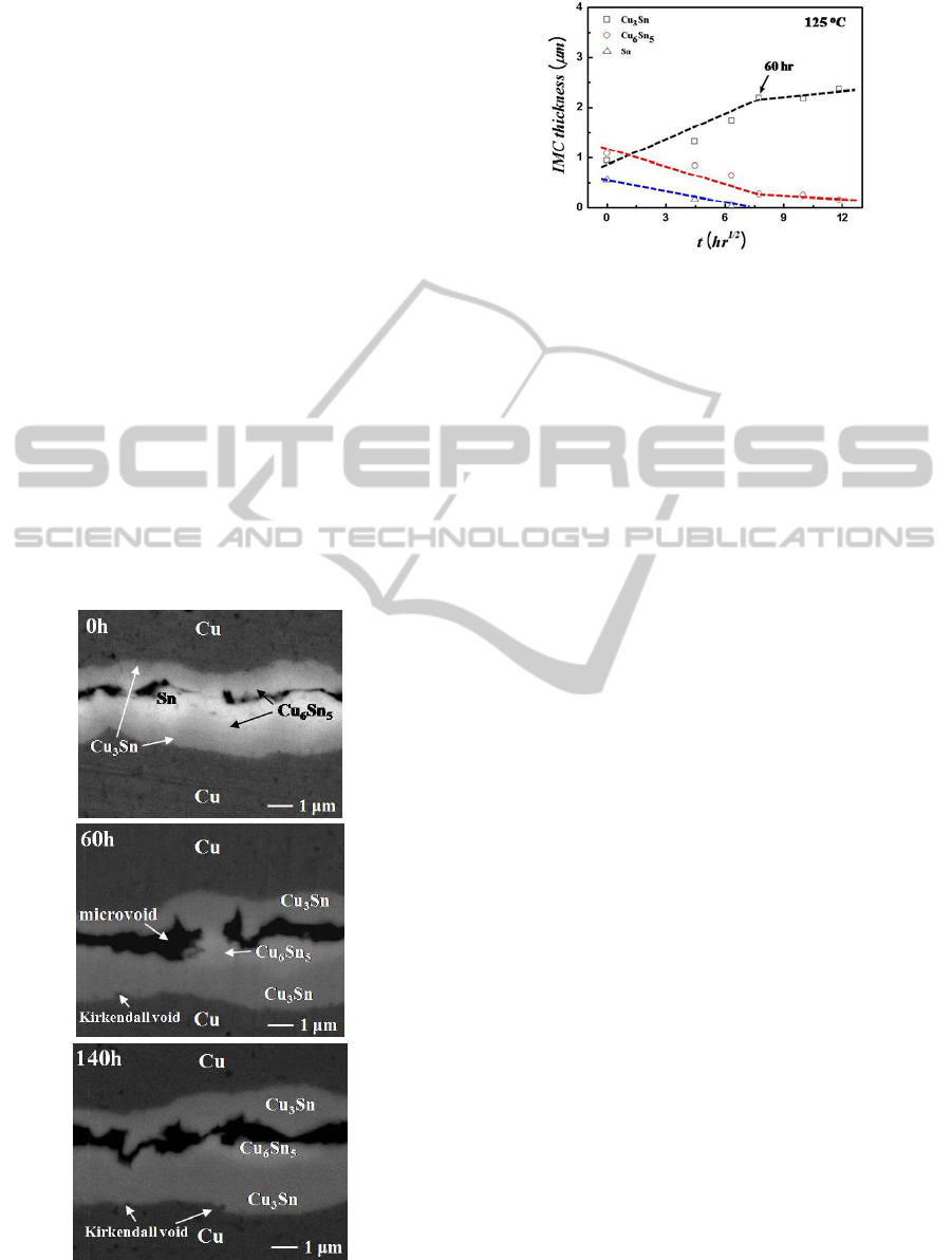
time. It has been reported that the Cu
6
Sn
5
and Cu
3
Sn
phases are generally formed at the Cu/Sn interface
during the reaction between Cu and Sn. Cu
3
Sn layer
on both interfaces have grown up with the similar
thicknesses. The Sn phase was not observed at the
Cu/Sn micro-bump interface after 60 h at 125. Fig. 3
shows the thickness of the IMCs as a function of the
square root of the annealing time at 125°C. The
growth of the IMC followed a linear relationship
with the square root of the annealing time. This
implies that the growth of the total IMC was
controlled by a diffusion mechanism. To understand
the variation of IMC growth slopes at 125℃, the
IMC thicknesses of the Cu
6
Sn
5
and Cu
3
Sn phases as
a function of the square root of the annealing time at
125℃. The Cu
6
Sn
5
and Cu
3
Sn phases linearly
increased together before 60 h at 125℃, and then the
Cu
6
Sn
5
phase rapidly decreased from initial at 125°C.
The Cu
3
Sn growth rate was also faster than the
Cu
6
Sn
5
growth rate compared with the Cu-Sn
reaction system of a conventional solder bump
structure, which is a Cu-limited system. This seems
to arise from the Cu/Sn micro-bump structure, which
is a Sn-limited system.
Figure 2: BSE micrographs of the enlarged cross-
sectioned Cu/Sn micro-bump during annealing at 125°C.
Figure 3: Intermetallic compound layer thickness with
annealing time at 125°C.
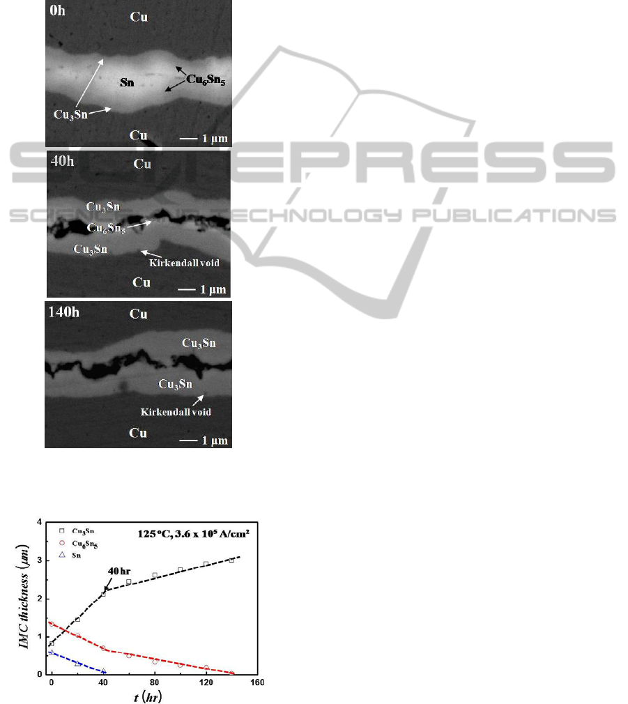
3.2 Interfacial Reaction Characteristics
during Electric Current Stressing
Electromigration test was performed with current
density of 3.6×10
4
A/cm
2
at 125℃. In order to
obtain the growth kinetics of IMCs in Cu/Sn micro-
bump, in-situ BSE images were taken from cross-
sectioned Cu/Sn micro-bump during current
stressing as shown in Fig. 4. The microstructural
observation results suggest that only Cu
6
Sn
5
was
observed at the Cu pillar/Sn interfaces and a few
micro-voids exist in the Sn phase just after reflow.
During current stressing, Cu
3
Sn phase grows at
Cu/Cu
6
Sn
5
interfaces and pure Sn phase disappears
after 40 h where the electron wind force seems to
enhance the IMC formation reaction between Cu and
Sn (Lee, Zhang, Wong, Tan, and Hadikusuma, 2006,
Chao, Chae, Zhang, Lu, Im, and Ho, 2007). Higher
temperature enhances the interfacial reaction which
leads to earlier consumption of pure Sn phase.
Therefore, the temperature as well as the electric
current accelerates the IMC reaction rate between
Cu and Sn. Figure 5 shows the IMC growth behavior
over current stressing time. It is noticeable that the
IMC thickness increases linearly with stressing. This
is closely related to different reaction kinetics of
electromigration compared to pure annealing. We
believe that there are competitions between diffusion
inside IMCs and chemical reaction at Cu/Sn
interface. After characteristic stressing time, the
IMC growth slope has sharply decreased, which can
be seen clearly from magnified BSE images in Fig.
4. Different bump structure and material systems
might lead to different reaction limiting systems.
4 CONCLUSIONS
The IMCs growths behaviors and electrical
reliability of Cu/Sn micro-bump in wafer level
ELECTRICAL RELIABILITY OF Cu/Sn MICRO-BUMP IN WAFER LEVEL PACKAGING FOR BioMEMS DEVICES
313
packaging for advanced BioMEMS devices
applications were systematically investigated by in-
situ SEM observation method. During current
stressing condition, IMC thickness increased linearly
with stressing time. It was observed that Cu
3
Sn
growth rate was larger than that of Cu
6
Sn
5
, which is
opposite result observed in conventional solder
bump. After the complete Sn exhaustion in the bump,
Figure 4: BSE micrographs of the cross-sectioned Cu/Sn
micro-bump during current stressing at 3.6×10
4
A/cm
2
and
125°C.
Figure 5: Intermetallic compound layer thickness with
current stressing time at 125°C and 3.6×10
4
A/cm
2
.
Cu
6
Sn
5
thickness became to decrease and Cu
3
Sn
grew faster. When current applied in Cu/Sn micro-
bump, IMC grew faster than annealing condition,
and the transition time of IMC growth was shortened,
and the transition time showed inverse proportional
to current density. Electrical Lifetime should be
correlated to this microstructural evolution during
current stressing.
ACKNOWLEDGEMENTS
This work was supported by joint research project of
Korea research council for industrial science and
technology of Korea Ministry of Knowledge
Economy.
The authors would like to thank Mr.
Kiwook Lee and Jaedong Kim at Amkor
Technology Korea Inc. for valuable sample
preparations and fruitful discussions.
REFERENCES
Chiang, K. N., Lee, C. C., Lee, C. C., and Chen, K. M.,
2006, Applied Physics Letters, vol. 88, pp. 072102_1-
3.
Rao, V. S., Tay, A. A. O., Kripseph, V., Lim, C. T., and
Yoon, S. W., 2004, in Proceedings of the 6th
Electronics Packing Technology Conference,
Singapore, Dec., pp. 444-449.
Son, H. Y., Jung, G. J., Park, B. J., and Paik, K. W., 2008,
Journal of Electronic Materials, vol. 37, pp. 1832-
1842.
Tu, K. N., Mayer, J. W., and Feldman, L. C., 1992, New
York: Macmillan, pp. 324.
Lee, T. K., Zhang, S., Wong, C. C., Tan, A. C., and
Hadikusuma, D., 2006, Thin Solid Films, vol. 504, pp.
441-445.
Chao, B., Chae, S. H., Zhang, X., Lu, K. H., Im, J., and Ho,
P. S., 2007, Acta Metallurgica et Materialia., vol. 55,
pp. 2805-2814.
BIODEVICES 2011 - International Conference on Biomedical Electronics and Devices
314
