
A MULTIBAND CMOS VCO WITH SWITCHING BONDWIRE
INDUCTOR FOR BIOMEDICAL WIRELESS FREQUENCY BAND
Design and Performance Analysis
Seonghan Ryu
Department of Information and Communication Engineering, Hannam University, Daejeon, South Korea
Keywords: Wireless Sensors, RF Transceiver, CMOS VCO, Biomedical Frequency Band.
Abstract: This paper presents a multiband low phase noise CMOS VCO with wide frequency tunability using
switched bondwire inductor bank, for operation in the medical wireless frequency band. The combination of
bondwire inductor and CMOS switch transistor enhances frequency tunability and improves phase noise
characteristics. All most of the medical wireless frequency bands can be covered by the single VCO
proposed in this paper. The proposed multiband VCOs, VCO1 operates from 2.3 GHz to 6.3 GHz with
phase noise of -136 and -122 dBc/Hz at 1 MHz offset frequency, respectively, and VCO2 operates from 4.9
GHz to 12.7 GHz with phase noise of -122.3 and -111.8 dBc/Hz at 1 MHz offset frequency, respectively.
Switched bondwire inductor bank shows high quality factor Q at each frequency band, which allows better
tradeoff between phase noise and power consumption. The proposed VCO1 is designed in TSMC 0.18um
CMOS process and consumes 7.2 mW power resulting in figure of merit(FOM) of -189.3 dBc/Hz at 1 MHz
offset from 6 GHz carrier frequency, and the proposed VCO2 is designed in SEC 65nm CMOS process and
consumes 8 mW power resulting in figure of merit(FOM) of -184.6 dBc/Hz at 1 MHz offset from 12 GHz
carrier frequency.
1 INTRODUCTION
These days, wireless technologies have been widely
used for medical applications including measuring
physiological signals, intelligent mobile emergency
response systems and patient monitoring both inside
and outside the hospital, etc. In biomedical
application, devices using wires are not suitable for
signal detection, record and transmission because
human behaviour is restricted by wires. Wireless
solution is also favored for infection free and
cosmetic point of view. Therefore, a single chip
solution including RF transceiver is becoming more
prevalent in biomedical application, considering size,
power consumption and economic issues. Among
the efforts for the single chip radio integration, the
low phase noise VCO implementation gets a lot of
attentions because the phase noise of the VCO is one
of the most critical parameters for the information
transfer achievement. A major challenge in the
single chip solution for biomedical application is the
establishment of low cost communication terminals,
which is highly integrated and can support multi-
band and multi-standards. Table 1 shows the
different frequency bands, which is used for medical
applications both on U.S. and Europe(Mohamed et
al, 2009).
Table 1: Summary of Medical Wireless Frequency Bands.
Location Frequency Band Frequency [MHz]
U.S.
Medical Implant
Communications
Service
402 - 405
U.S.
Wireless Medical
Telemetry Service
608 - 614
1395 – 1400
1427 - 1432
U.S.
Instrumentation,
Scientific, and
Medical (ISM)
315
902 - 928
2400 - 2483.5
5150 - 5875
Europe ISM
433.05 – 434.79
868 – 870 (short -range)
2400 – 2483.5
U.S. UWB
3.1 – 10.6 GHz
22 - 29 GHz, center
freq > 24.075 GHz
Europe UWB
4.2 – 4.8 GHz
6 – 8.5 GHz
3.4 – 4.2 GHz (Pending)
Multiband radio using multiple transceivers can
satisfy these demands, however the complexity and
323
Ryu S..
A MULTIBAND CMOS VCO WITH SWITCHING BONDWIRE INDUCTOR FOR BIOMEDICAL WIRELESS FREQUENCY BAND - Design and
Performance Analysis.
DOI: 10.5220/0003133303230328
In Proceedings of the International Conference on Biomedical Electronics and Devices (BIODEVICES-2011), pages 323-328
ISBN: 978-989-8425-37-9
Copyright
c
2011 SCITEPRESS (Science and Technology Publications, Lda.)

chip area should be increased. Though design
research for RF building blocks with wide frequency
operability has been progressed, single low phase
noise multiband CMOS VCO design is still remain
as challenging work (S. Ryu et al, 2005), (K. Lee et
al, 2008). The multiband VCO with wide frequency
tunability needs large capacitor banks and varactor
diodes, large capacitor banks results area occupation
issue and high VCO gain of varactor results phase
noise degradation issue. Though these problems can
be solved by allowing higher power consumption,
this is not desirable for biomedical application which
requires low power consumption for long lifetime of
implantable and wearable devices.
This paper describes design of a low phase noise
CMOS VCO with very wide frequency tunability
using switched bondwire inductor bank. All most of
the medical wireless frequency bands can be covered
by the single CMOS VCO proposed in this paper,
with just simple divide-by-two prescaler.
With a 1.2 V power supply, this VCO1 consumes
a 6 mA bias current at VCO core and shows
frequency tunability from 2.3 to 6.3 GHz, and VCO2
consumes a 6.7 mA bias current at VCO core and
shows frequency tunability from 4.9 to 12.7 GHz
with low phase noise characteristics
2 MULTIBAND VCO ISSUE
Multiband multi-standard RF transceiver for
biomedical application requires the LO block with
very wide tuning range and low phase noise,
therefore LO block structure based on only divide-
by-two prescaler is favored these days, since side
effects of other structures such as self-mixing, DC-
offset and frequency pushing/pulling can be
minimized. In addition, this simple LO chain
structure is the optimum solution to minimize the
cost in terms of system complexity, power
consumption and area in comparison with other
solutions such as quadrature VCO (QVCO) and a
polyphase filter (A. Koukab et al, 2006). For this
simple LO structure, VCO core itself should have
very wide tuning range. A usual way to achieve a
wide tuning range is adopting a switched capacitor
bank in a VCO resonator for coarse tuning. For fine
tuning, a large varactor with high VCO gain, K
vco
,
also helps to enlarge VCO frequency tuning band.
However, smaller varactor with low K
vco
enables
low phase noise and switched capacitor bank is more
suitable for small frequency changes (Z. Li et al,
2005). Therefore the utilization of both capacitor
and inductor switching can be an optimum solution
for wide frequency tunability. The switched inductor
bank can be composed of planar spiral inductors and
MOS switch (S. Yim et al, 2006).
Considering the size and Q factor of the on-chip
spiral inductor, single-turn inductor of about 1 nH is
favored for 2 ~ 6 GHz operation. A custom -
designed single - turn inductor shows Q
of around 15
~ 20. However, relatively large inductor size, out -
diameter of around 400 ~ 500 µm, is required.
Switched inductor bank with these inductors is not
desirable solution due to area issue. The proper sized
conventional planar spiral inductor of CMOS
process provides Q of about 10. Therefore, VCO
phase noise characteristics may be severely
degraded by switched inductor bank using
conventional spiral inductor due to MOS switch
parasitics, such as on resistance, R
on
.
3 LOW PHASE NOISE VCO
WITH BONDWIRE
To resolve this problem, bondwire inductor is
proposed in this work. Bondwire inductor shows
good quality factor above 25 in the frequency range
of interest. The inductance of bondwire structure is
linearly increased with the bondwire length and can
be modified with changing the distance between two
bondpads and bondwire height. We have recently
reported a bondwire inductor VCO with low phase
noise characteristics (K. Lee et al, 2008). This VCO
exhibits good phase noise performance while
simultaneously achieving enough tuning range.
Though the variation of the bondwire inductance is
higher than that of on-chip spiral inductor, more than
20% of the inductance value can be tuned even after
chip fabrication by inserting dummy tuning pads in
circuit layout and changing bondwire length or
height. Therefore, the bondwire inductor VCO is one
of the best solutions for low noise and low cost RF
transceiver of biomedical devices.
4 DESIGN OF THE TEST
VEHICLE: MULTIBAND VCO
WITH SWITCHING
BONDWIRE INDUCTOR
The proposed VCO adopts a switched bondwire
inductor bank, which is composed of three bondwire
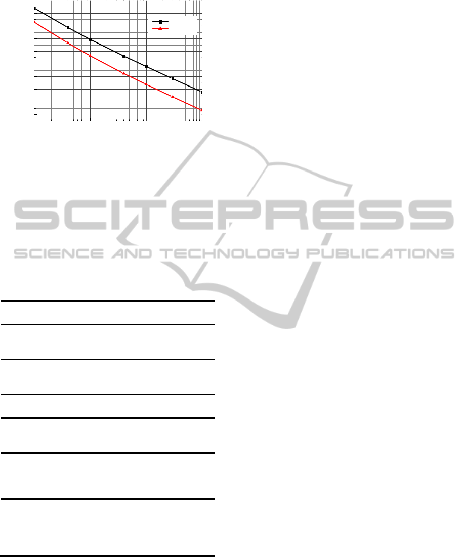
inductors with different length. Fig. 1 and Fig. 2
shows simulated inductance value and Quality factor
BIODEVICES 2011 - International Conference on Biomedical Electronics and Devices
324
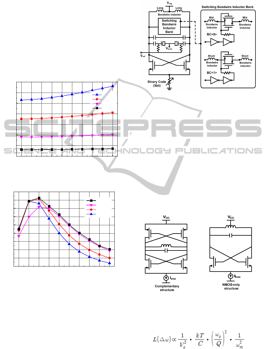
of the bondwire inductor, respectively. 3D - EM
simulator, HFSS is used for this characterization. In
these figures, _long, _mid and _short exhibit
bondwire inductor simulation results for length of
700, 525 and 350 um respectively, and _all depicts
simulation results for shunt connection of all three
bondwire inductors. As depicted in Fig. 2, the
frequency for maximum Q factor can be varied with
bondwire inductance switching, which can improve
VCO phase noise characteristics at each frequency
band.
1G 2G 3G 4G 5G 6G 7G 8G 9G 10G
200.0p
400.0p
600.0p
800.0p
1.0n
1.2n
1.4n
1.6n
L [H]
Frequency [GHz]
L_long
L_mid
L_short
L_all
Figure 1: Simulated inductance of switched bondwire
inductor.
1G 2G 3G 4G 5G 6G 7G 8G 9G 10G
4
8
12
16
20
24
28
32
36
40
Quality Factor
Frequency [GHz]
Q_all
Q_short
Q_mid
Q_long
Figure 2: Simulated Q factors of switched bondwire
inductor.
The proposed VCO structure is shown in Fig. 3. An
accumulation-type MOS varactor is used for fine
tuning. A switched bondwire inductor bank is used
for wide frequency tenability.
As depicted in Fig. 3, mid and short length
bondwire inductors are shunt - connected to long
bondwire inductor when all MOS switches are on
state, and switched inductor bank has lowest total
inductance value in that case. When all MOS
switches in switched inductor bank are off, mid and
Figure 3: Proposed VCO structure with bond-wire
inductors.
short length bondwire inductors are disconnected
and highest inductance value can be achieved.
Though bondwire inductors are connected through
MOS switches at on state, the Q factor degradation
from MOS R
on
resistance can be mitigated due to
shunt connection with long bondwire inductor which
is directly connected to VCO oscillation node
without MOS switch.
To design a wide frequency tuning range VCO
with good phase noise performance and low power
dissipation, a complementary structure and an
NMOS-only structure are compared. These two
types depicted in Fig. 4 are mostly favored for
differential CMOS VCO.
Figure 4: Comlementary and NMOS-only VCO structure.
The well-known phase noise model for an
oscillator is Leeson’s proportionality (D. B. Leeson
et al, 1966).
Where the phase noise is given by kT/C noise that
is shaped in frequency domain by LC tank and
A MULTIBAND CMOS VCO WITH SWITCHING BONDWIRE INDUCTOR FOR BIOMEDICAL WIRELESS
FREQUENCY BAND - Design and Performance Analysis
325
normalized to the power in the tank. This expression
reveals the dependency of the phase noise upon the
signal amplitude V
o
. For the complementary type
VCO, as the bias current increases, signal amplitude
is limited by V
DD
in the voltage limited regime,
while the NMOS-only type VCO enables higher
voltage swing above V
DD
limit. Therefore, the phase
noise of the complementary type at each offset
frequency may become worse than that of the
NMOS-only type as the bias current increases(S.
Ryu, 2009).
0246810121416
0.0
0.4
0.8
1.2
1.6
Phase Noise [dBc/Hz] @ 400 KHz Offset
VCO voltage swing [V]
Bias current [mA]
Complementary Vswing
NMOS Only Vswing
-124
-122
-120
-118
-116
-114
-112
-110
-108
Complementary PN
NMOS Only PN
Figure 5: Simulated VCO voltage swing amplitude and
phase noise at 400 KHz offset from 4GHz carrier
frequency as a function of bias current.
Although the complementary type still maintains
better phase noise performance for relatively small
bias current, below 4 mA, with V
DD
of 1.2V as
depicted in Fig. 5, this bias current is not enough to
satisfy the requirements for multi-band/multi-
standard operation. In addition, considering various
lossy components of the real circuits, enough phase
noise margin is necessary. Accordingly, the NMOS-
only type is adopted.
For minimizing power consumption, the VCO
bias current is varied between each frequency band
by controlling the 3-bit binary weighted bias
resistors. This programmability allows the trade-off
between power consumption and phase noise, which
is necessary for multi-band/multi-standard VCOs.
Considering these multiband low phase noise
VCO design issues, the proposed VCOs, VCO1 and
VCO2 is designed in 0.18 μm and 65nm CMOS
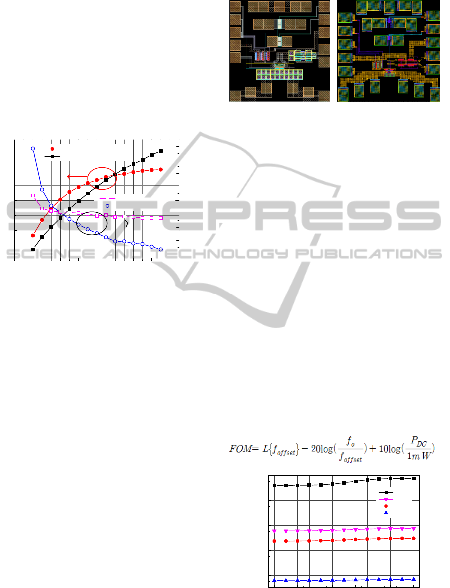
technology, respectively. Fig. 6 shows the complete
layout of the VCOs. The chip size is 0.75 × 0.75
mm
2
for each.
(a) VCO1, 0.18um TSMC (b) VCO2, 65nm SEC
Figure 6: Complete layout of the proposed CMOS VCO.
5 SIMULATION RESULTS
The carrier signal frequency of the VCO1 is tunable
between 2.28 GHz and 2.33 GHz when all MOS
switches are at off state, and when all MOS switches
are at on state, the carrier signal frequency is tunable
between 6.1 GHz and 6.38 GHz. The frequency
band between 2.33 GHz and 6.1 GHz can be covered
by controlling each MOS switch in the inductor
bank, separately. The full tuning range can also be
covered by utilizing both switched capacitor bank
and switched inductor bank. Fig. 7 and Fig. 8 depict
the simulated frequency tuning range and the phase
noise for the VCO1. The VCO1 exhibits a phase
noise of -127 and -136 dBc/Hz at 400 KHz and 1
MHz offsets from the 2.3 GHz Carrier. For the 6.2
GHz carrier, a phase noise of -113.8 dBc/Hz and -
122 dBc/Hz at 400KHz and 1MHz offsets are
attained, respectively. The VCO core operates from
1.2V supply and biases at 6 mA.
The simulation results of both VCO1 and VCO2
are summarized in table 1.
A widely used figure of merit (FOM) (A.
Waemans et al, 1998) for the VCO is defined as
0.00.20.40.60.81.01.21.41.61.82.02.22.4
2.0G
2.5G
3.0G
3.5G
4.0G
4.5G
5.0G
5.5G
6.0G
6.5G
Oscillation Frequency [Hz]
VCO tunin
g
volta
g
e
[
V
]
band4
band3
band2
band1
Figure 7: Simulated frequency tuning range of the
proposed VCO1.
BIODEVICES 2011 - International Conference on Biomedical Electronics and Devices
326
10k 100k 1M 10
M
-160
-150
-140
-130
-120
-110
-100
-90
-80
-70
Phase Noise [dBc/Hz]
Frequency Offset [Hz]
6.2 GHz
2.3 GHz
Figure 8: Simulated phase noise of the proposed VCO1 at
2.3 and 6.2 GHz carrier frequency.
Here, L{f
offset
} is the measured phase noise at
offset frequency f
offset
from the carrier frequency f
o
.
P
DC
is VCO power consumption in mW. The worst
simulated FOMs for the VCO1 and VCO2 are -
189.3 dBc/Hz at 6 GHz and -184.6 dBc/Hz at 12
GHz carrier frequency, respectively. Table 2. shows
the summary of the simulation results compared to
those of other low phase noise VCOs.
Table 2: VCO performance summary and comparison.
VCO Tech.
Freq.
[GHz]
Power
[mW]
P/N
[dBc/Hz]
FOM
Ham
2001
0.35um
Bi-
CMOS
1.91 10
-121
@600KH
z
-181.1
Astis
2005
0.35um
Bi-
CMOS
5.6 13.5
-117
@1MHz
-180.7
Fong
2003
0.13um
CMOS
3.0-5.6 2
-114.5
@1MHz
-186.5
Adrea
nj
2001
0.35um
CMOS
2.19 12.6
-139
@3 MHz
-185.3
VCO1
0.18um
CMOS
2.28-2.33
3.88-3.91
4.27-4.31
6.10-6.38
7.2
-122
@1 MHz
[ 6GHz]
-189.3
VCO2
65nm
CMOS
4.93-5.07
8.34-8.60
9.48-9.75
12.21-
12.74
8.0
-111.8
@1 MHz
[12GHz]
-184.6
6 CONCLUSIONS
In this work, a low phase noise, multiband CMOS
VCO for biomedical wireless frequency bands, with
wide frequency tunability through switching
bondwire inductor, has been presented. All most of
the medical wireless frequency bands can be covered
by the single CMOS VCO proposed in this paper.
The design has been achieved with TSMC 0.18
μm and SEC 65nm CMOS process. An NMOS-only
structure and high Q bond wire inductor are adopted
for enough phase noise margin, wide frequency
tunability, and chip area efficiency. In addition,
programmable 3-bit bias resistors are used for a
trade-off between phase noise and power
consumption. Proposed switched bondwire inductor
bank is composed of CMOS switch and bondwire
inductors, which enable very wide frequency
tunability and low phase noise characteristics.
The simulation results show that the tuning ranges
are from 2.3 GHz to 6.4 GHz for VCO1 and from
4.9 GHz to 12.7 GHz for VCO2. The phase noise
performance of the VCO1 is -122 dBc/Hz at 1 MHz
offset from the 6 GHz Carrier. For the VCO 2, a
phase noise of -111.8 dBc/Hz at 1MHz offset from
12 GHz carrier is achieved. The simulated FOM for
the VCOs are -189.3 dBc/Hz and -184.6 dBc/Hz for
VCO1 and VCO2, respectively. These FOM values
confirm that a good tradeoff among phase noise,
wide tunability and power consumption is achieved
from the proposed CMOS VCOs.
REFERENCES
Mohamed R. Mahfouz, “Integration of UWB and Wireless
Pressure Mapping in Surgical Navigation,” IEEE
Trans. Microw. Theory Tech. vol. 57, no. 10, pp.
2550-2564, Oct.2009.
S. Ryu, Y. Chung, H. Kim, J. Choi, and B. Kim, “Phase
noise optimization of CMOS VCO through harmonic
tuning,” in IEEE Radio Freq. Integr. Circuits Symp.,
Long Beach, CA. pp. 403–406, Jun. 2005.
K. Lee, H. Yu, H. Ahn, H. Oh, S. Ryu, D. Keum and B.
Park, “A0.13-um CMOS Σ-Δ Frequency Synthesizer
with an Area Optimizing LPF, Fast AFC Time, and a
Wideband VCO for WCDMA/GSM/GPRS/ EDGE
Applications,” in IEEE Radio Freq. Integr. Circuits
Symp., Atlanta, GA. pp. 299–302, Jun. 2008.
A. Koukab, Y. Lei, M. J. Declercq, “A GSM-
GPRS/UMTS FDD-TDD/WLAN 802.11a-b-g Multi-
Standard Carrier Generation System,” IEEE J. Solid-
State Circuits, vol. 41, pp. 1513-1521, July. 2006.
Z. Li and K.K.O, “A Low-Phase-Noise and Low-Power
Multiband CMOS Voltage-Controlled Oscillator,”
IEEE Trans. Microw. Theory Tech. vol. 40, no. 6, pp.
1296-1302, Jun. 2005.
S. Yim and K.K.O, “Switched Resonators and Their
Applications in a Dual-Band Monolithic CMOS LC-
Tuned VCO, ” IEEE Trans. Microw. Theory Tech.,
A MULTIBAND CMOS VCO WITH SWITCHING BONDWIRE INDUCTOR FOR BIOMEDICAL WIRELESS
FREQUENCY BAND - Design and Performance Analysis
327

vol. 54, no. 1, pp. 74-81, Jan. 2006.
D. B. Leeson, “A Simple Model of Feedback Oscillator
Noise Spectrum,” Proceedings of the IEEE, vol. 54,
pp. 329–336, 1966.
S. Ryu, “Multi-standard carrier generator with CMOS
logic divider,” in IEEE Int. Midwest Symp on Circuit
and Systems., Cancun. pp. 1059–1062, Aug. 2009.
A. Wagemans, “A 3.5 mW 2.5 GHz diversity receiver and
a 1.2 mW 3.6 GHz VCO in silicon-on-anything,”
IEEE Int. Solid-State Circuits Conf. Tech. Dig., pp.
250-251, Feb. 1998.
D. Ham and A. Hajimiri, “Concepts and methods in
optimization of integrated LC VCOs,” IEEE J. Solid-
State Circuits, vol. 36, pp. 896–909, Jun. 2001.
G. De Astis, D. Cordeu, J. Paillot, and L. Dascalescu, “A
5-GHz fully integrated full pMOS Low-phase-noise
LC VCO,” IEEE J. Solid-State Circuits, vol. 40, pp.
2087–2091, Oct. 2005.
N. Fong, “Design of wideband CMOS VCO for multiband
wireless LAN applications,” IEEE J. Solid-State
Circuits, vol. 38, pp. 1333–1342, Aug. 2003.
P. Adreanj and H. Sjoland, “A 2.2 GHz CMOS VCO with
inductive degeneration noise suppression,” in Proc.
IEEE Custom Integrated Circuit Conf., San Diego,
CA, pp. 197–200, May. 2001.
BIODEVICES 2011 - International Conference on Biomedical Electronics and Devices
328
