
AN INTEGRATED MULTI-CHANNEL SYSTEM FOR
BIOMEDICAL SIGNAL ACQUISITION
Jakob M. Tomasik, Wjatscheslaw Galjan, Kristian M. Hafkemeyer
Dietmar Schroeder and Wolfgang H. Krautschneider
Institute of Nanoelectronics, Hamburg University of Technology, Eissendorfer Str. 38
D-21073 Hamburg, Hamburg, Germany
Keywords: Biomedical signals, SoC, Low-power, Low-noise, Configurable, CMRR-calibration, DC-suppression.
Abstract: A CMOS configurable system-on-chip (SoC) for biomedical signal acquisition is described. The SoC is
composed of 10 channels, each channel including a programmable analog front-end (AFE) and a 20 bit
analog-to-digital converter (ADC). The digitized signals are read out via a high-speed serial communication
bus. The AFE includes a common-mode rejection ratio (CMRR) calibration circuitry resulting in a CMRR
of more than 80 dB and an active DC-suppression circuitry giving the DC-coupled instrumentation
amplifier the possibility to tolerate DC-offsets of up to ±1 V for a power supply voltage of 3.3 V. In low-
noise mode the AFE achieves an input referred noise of less than 50 nVrms for EEG application (0.5-70 Hz)
and the power consumption of a channel including AFE and ADC is less than 5 mW in low-power mode. A
prototype has been fabricated in a 0.35 µm CMOS process.
1 INTRODUCTION
The integration of biomedical signal acquisition
systems in CMOS technology allows not only a
reduction of costs for traditional medical devices,
but also facilitates portable long-term applications or
implantable solutions. As part of an integrated
solution, designs of a complete analog front-end
(AFE) have been reported (Martins et al., 1998; Ng
and Chan, 2005; Yazicioglu, 2007). In addition,
Desel et al. (1996) and Fuchs et al. (2002) describe
system-on-chip (SoC) implementations including
also analog-to-digital conversion (ADC) and digital
IO interfacing.
To cover the wide range of biomedical signals
the system should be adaptable to their
characteristics. The flexibility of a system means to
provide an optimal setting of the overall system with
respect to the signal type and system application. In
this context, the AFE is the prime candidate for
configurability. Two complementary application
examples illustrate this: For portable long-term
monitoring of electrocardiogram (ECG) signals the
system’s power consumption plays an essential role
whereas noise constraints are rather relaxed (Martin
et al., 2000; Galjan et al., 2008). In contrast to this,
for extremely sensitive evoked potential (EP)
recordings (Scheer et al., 2006), low-noise amplifi-
cation of the signal is crucial at the expense of rather
high power consumption. Including these two
extreme settings, a configurable biomedical signal
acquisition system should be adaptable to a variety
of signal types. Table 1 shows the associated signal
characteristics based on (Bronzino, 2000; Webster,
1998).
Table 1: Characteristics of biomedical signals.
Signal
Type*
Signal Bandwidth Signal Amplitude
ECG 0.05 Hz–250 Hz 5 µVpp – 8 mVpp
EEG 0.05 Hz – 70 Hz 2 µVpp – 200 µVpp
EMG 0.01 Hz – 5 kHz 50 µVpp – 10 mVpp
EP 0.1 Hz – 3 kHz 20 nVpp – 20 µVpp
*
ECG: electrocardiogram, EEG: electroencephalogram,
EMG: electromyogram, EP: evoked potentials.
Two additional requirements are inherently
typical for biomedical signal acquisition systems: A
high common-mode rejection ratio (CMRR) (in
particular at 50/60 Hz) and large electrode DC-offset
handling capability. The need for a high CMRR
results from power line interferences inducing a
common mode voltage present at the amplifier’s
36
Tomasik J., Galjan W., Hafkemeyer K., Schroeder D. and Krautschneider W..
AN INTEGRATED MULTI-CHANNEL SYSTEM FOR BIOMEDICAL SIGNAL ACQUISITION.
DOI: 10.5220/0003137600360045
In Proceedings of the International Conference on Biomedical Electronics and Devices (BIODEVICES-2011), pages 36-45
ISBN: 978-989-8425-37-9
Copyright
c
2011 SCITEPRESS (Science and Technology Publications, Lda.)
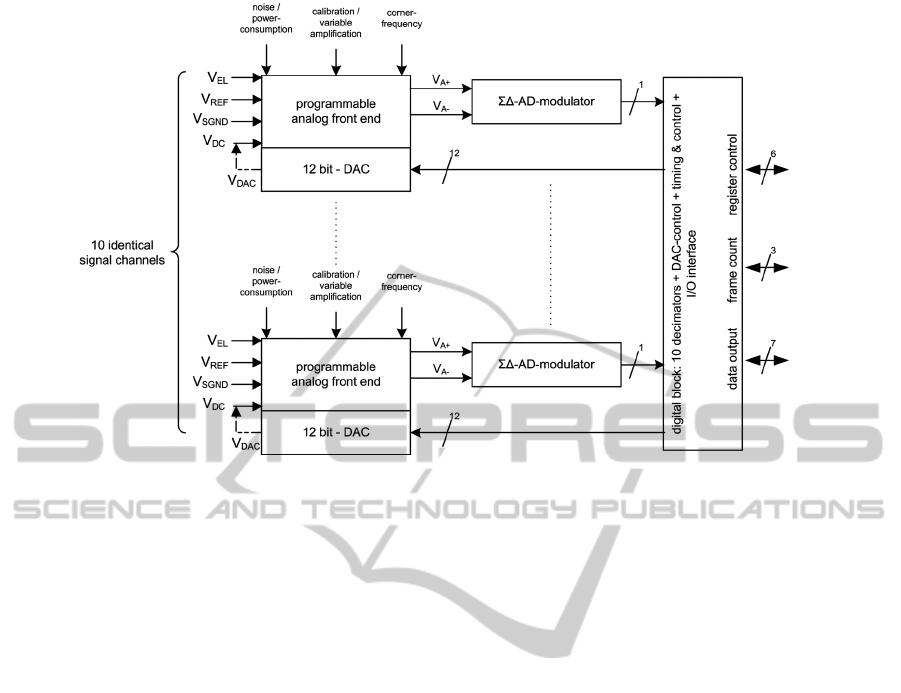
Figure 1: Block diagram of the system-on-chip.
input (Webster, 1998). Large DC-offsets (i.e.
hundreds of millivolts) may arise from the electrode-
skin interface (Webster, 1998) and require counter
measures to prevent saturation of the instrumen-
tation amplifier (IA). Finally, a biomedical SoC
should provide a digital interface for simple
configuration of the system and a high speed data
output for read out of the acquired biomedical
signals.
In this work we present a configurable SoC for
biomedical signal acquisition including CMRR-
calibration and DC-offset suppression. A first
approach for the SoC has been described in (Van
Helleputte et al., 2008) and first simulation results of
this system have been presented in (Hafkemeyer et
al., 2007). This paper is organized as follows:
Section 2 gives an overview of the system. In
Section 3 we describe the analog front-end, in
Section 4 the analog-to-digital converter is pre-
sented, and in Section 5 the digital IO interface is
described. In Section 6 we present the measurement
results and discussion and conclusion are finally
contained in Section 7.
2 SYSTEM OVERVIEW
The block diagram of the SoC is presented in
Figure 1. The main components of this SoC are 10
identical channels and a digital block. Each channel
includes an AFE, a ΣΔ-modulator and a 12-bit
digital-to-analog converter (DAC) for DC-offset
suppression of the associated channel. The AFE’s
inputs are the electrode input (V
EL
), the reference
signal (V
REF
), signal ground (V
SGND
) and DC-
suppression voltage (V
DC
). Whereas V
EL
, V
REF
and
V
SGND
are familiar IA inputs, the V
DC
input is used
to suppress the input DC-offset voltage and is driven
by the DAC output (V
DAC
).
Subsequent to the AFE the ΣΔ-modulator
generates a 1-bit stream which is decimated to
perform the analog-to-digital conversion. The digital
block contains 10 decimation filters for this purpose.
Additional functions of the digital block include the
control of the DAC, timing and SoC’s sub blocks.
Finally, the digital block enables communication to
and from the chip. This comprises setting the
internal registers (register control), reading out the
measured data (data output) and synchronizing the
measured data if several chips are used on the same
bus (frame count).
3 ANALOG FRONT-END
A block diagram of the programmable analog front-
end is given in Figure 2a. The IA amplifies the
applied signal with a constant factor of 4. The signal
is fed into the postamplifier directly or via an
external high-pass filter.
The postamplifier’s gain is configurable with
amplification factors of 5, 20, 40 and 80 resulting in
the desired channel gain factors of 20, 80, 160 and
320. Following the postamp a low-pass filter acts as
AN INTEGRATED MULTI-CHANNEL SYSTEM FOR BIOMEDICAL SIGNAL ACQUISITION
37

Figure 2: (a) Structure of the programmable analog
front-end, (b) detailed view of the IA.
an anti-aliasing filter for the ADC. The low-pass
corner frequency can be set to be either 3 kHz (ECG,
EEG) or 15 kHz (EMG, EP). Finally, the single-
ended signal is converted to a differential one as
required by the subsequent ΣΔ-modulator. The
design specifications for the AFE are given in
Table 2.
3.1 Instrumentation Amplifier with
CMRR-calibration
The IA used as a preamplifier in the AFE is
implemented by using a modified 2-opamp IA
architecture and is presented in Figure 2b. The
modification is composed of a third opamp for
subtracting any DC-offset using the DAC generated
voltage V
DC
. The additional circuitry also incorpo-
rates a digitally controlled tunable resistor for
CMRR-calibration, the resistor’s step size is denoted
as ΔR. For modeling parasitic PCB or bond wire
resistances at the signal ground input V
SGND
a
resistor R
PCB
has been added in Fig 2b. The IA’s
transfer function with respect to V
SGND
is given by:
. and with
EL
PCBAA
A
DC
B
REF
BA
HPOUT
RRRRnRR
R
R
V
R
R
R
R
V
R
R
R
R
VV
+=Δ⋅+=
−
⎟
⎟
⎠
⎞
⎜
⎜
⎝
⎛
+−
⎟
⎟
⎠
⎞
⎜
⎜
⎝
⎛
++=
4411
1
2
4
3
1
2
1
2
1
2
11
**
*
**
,
(1)
A differential gain G between V
EL
and V
REF
is
obtained from (1) by setting the values for R
1
, R
2
, R
3
Table 2: Design specifications for the analog front-end.
Parameter Conditions/Remarks Value
Signal
input
range
Ext. programmable ± 5 mV
± 20 mV
± 40 mV
± 80 mV
Offset
comp.
range
0.01 Hz – 5 kHz ± 1000 mV
@ VDD = 3.3
V
Total
input
referred
noise
0.05 Hz – 250 Hz (ECG)
0.05 Hz – 70 Hz (EEG)
0.01 Hz – 5 kHz (EMG)
0.1 Hz – 3 kHz (EP)
< 4.7 µVpp
< 1.0 µVpp
< 6.0 µVpp
< 2.2 µVpp
CMRR @ 50 Hz > 80 dB
and R
4
(neglecting R
PCB
and assuming R
1
= R
1A*
=
R
1B
and V
DC
= 0 V) such that the terms in front of
V
EL
and V
REF
have both the same value G. In this
case the gain G is equal to
.
2
1
4
3
1
2
2
R
R
R
R
R
R
VV
V
G
E
L
HPOUT
−+=
−
=
REF
(2)
In the presented circuit a gain value of G = 4 has
been obtained by using resistor values of R
1
= 1 kΩ,
R
2
= 1.5 kΩ, R
3
= 1 kΩ and R
4
= 600 Ω.
If any DC-offset is present at the input, the
aforementioned voltage V
DC
scaled by a factor
R
2
/R
1A
is subtracted from the IA’s output voltage
V
HPOUT
. The result of this action is a cancellation of
DC-offsets up to a value of
.
,
1
2
2 R
R
G
V
V
DD
dcmaxEL
=
(3)
Using above values for R
1
, R
2
and G and a power
supply voltage V
DD
of 3.3 V, a maximal DC-offset
of V
EL,dcmax
= ± 619 mV is obtained. In conjunction
with the external high pass filter and a postamplifer
gain of 80 the specified offset compensation range
of ± 1000 mV is reached.
The CMRR calibration compensates for any
mismatch in the resistors R
1
to R
4
and wiring
parasitics R
PCB
. The calibration circuit has been
located in the high-resistive feedback loop of the
DC-offset compensation opamp to minimize non-
idealities. By changing the tap-point in the feedback
path of the DC-offset compensation opamp a value
of nΔR is added to the resistor R
1A
. The CMRR of
the IA becomes
.
11
1
4
3
1
2
1
2
1
2
⎟
⎟
⎠
⎞
⎜
⎜
⎝
⎛
+
Δ±
+
+
Δ±
+
=
R
R
RnR
R
R
R
RnR
R
CMRR
A
BA
(4)
BIODEVICES 2011 - International Conference on Biomedical Electronics and Devices
38

It should be taken into account that a variation of
R
1A
also affects the differential gain G. Therefore
resistor values should be chosen such that the gain
error between channels does not exceed 1%. A
CMRR value of more than 80 dB (including R
PCB
) is
achieved by using a step size ΔR < 0.26 Ω and n =
64 steps. Using a driven right leg system (Winter,
1983) for patient grounding the overall CMRR is
increased by approx. 40 dB resulting in a system
CMRR of 120 dB.
The configurability of the IA regarding
noise/power- consumption is realized using the
programmable operational amplifier described in
(Bronskowski and Schroeder, 2006). These opamps
use chopper modulation to reduce 1/f-noise and can
be programmed in a wide range between ultra low-
noise (2 nV/√Hz) and low-power consumption
(140 µW).
3.2 Postamplifier and External
Highpass Filter
The postamplifier is composed of the same
programmable opamp as the IA. It is used in a non-
inverting configuration having four gain settings (5,
20, 40 and 80). These are realized by a resistor chain
having four taps. Connecting one of the taps to the
opamp’s inverting input using a CMOS switch sets
the appropriate gain factor. Care has to be taken
regarding the accuracy of the resistors to fulfill the
specified gain error between channels (<1%).
Chopper modulation of the opamp is also needed in
the postamplifier due to the low preamplifiers’s gain
factor of 4 for low-noise applications.
The optional external passive high pass filter can
be placed between the V
HPOUT
output pin of the IA
and the postamplifier’s input pin V
HPIN
(dashed line
in Figure 2a). Using external components for the
high pass filter (i.e. capacitor and resistor) eases the
implementation of the large time constants needed.
A drawback of the large time constant arises if
events like external stimulation or movements of the
electrodes induce a noticeable shift in the DC-
potential of the external capacitor: the time for
restoring the system back to equilibrium is
determined by the time constant of the high pass
filter, i.e. in range of seconds. To overcome this
problem an additional switch has been placed to
discharge the capacitor over the relative small
resistor R
Block
. The signal to close the switch (“block
enable” in Figure 2a) can be set via the serial
configuration port.
3.3 Low-pass Filter and Symmetry
Stage
The ΣΔ-analog-to-digital conversion requires an
anti-aliasing filter preceding the ΣΔ-modulator. In
contrast to Nyquist-rate ADCs the anti-aliasing
filter’s cut-off frequencies are rather easy to
implement with oversampling ADCs, where the
relative low bandwidths of the biomedical signals
would lead to large time constants and hence require
external components. The anti-aliasing filter is
implemented as a second-order low-pass filter using
an opamp in a Sallen&Key configuration (Allen and
Holberg, 2002). To choose the cut-off frequency, the
maximum signal frequency, the oversampling ratio
and the needed signal attenuation have to be
considered. Choosing an attenuation of more than
40 dB at half of the oversampling frequency and an
oversampling ratio of 256, cut-off frequencies of 3
kHz for ECG/EEG and 15 kHz for EMG/EP ensure
proper anti-aliasing functionality. The cut-off
frequency can be configured externally via the serial
configuration port.
Following the low-pass filter a symmetry stage
converts the single-ended signal (V
A+
) into a
differential one using an opamp to obtain the
inverted signal (V
A-
). These signals are fed into the
succeeding ΣΔ-modulator. Additional care has to be
taken to keep these signals stable at the modulators
input because of its switching operation (Maxim
Integrated Products, 2000). Therefore, an integrated
low-path RC-filter with R = 5 kΩ and C = 2.5 pF has
been inserted between the symmetry stage outputs
and the ΣΔ-modulator inputs.
4 ADC
Analog-to-digital conversion for each channel is
accomplished by a 2
nd
-order ΣΔ-modulator and a
decimation filter. The default oversampling ratio
(OSR) of the ΣΔ-modulator is 256, the OSR can be
changed using the serial configuration port to a
value of OSR = 256 ± 128 (in steps of 1). The sam-
pling rate at the modulator’s input is derived from
the 12.8 MHz main clock using on-chip division by
(n + 1). Like the OSR, n can be set by programming
and has a value range from n = 0 to n = 255. For
example, using an oversampling ratio of 256 and
setting n to 0 or 249 data rates (DR) of 50 kHz and
200 Hz can be achieved, respectively.
AN INTEGRATED MULTI-CHANNEL SYSTEM FOR BIOMEDICAL SIGNAL ACQUISITION
39
4.1 Sigma-Delta Modulator
The 2
nd
-order ΣΔ-modulator is implemented as a
discrete time 1-bit modulator. The circuit topology
of the switched-capacitor ΣΔ-modulator is derived
from (Medeiro et al., 1997) and a modified version
also used in the present topology has already been
used in (Fuchs et al., 2002). The sizing of the actual
capacitors used for the switched capacitor
integrators results in signal-transfer and noise-
transfer functions (STF and NTF) (Fuchs, 2004):
7148
1
)(
2
+−
=
zz
zSTF
(5)
and
.
7148
8168
)(
2
2
+−
+−
=
z
z
zz
zNTF
(6)
The required effective number of bits (ENOB) of
the ΣΔ-modulator is depending on the signal type:
For EEG approx. 16 bits or a dynamic range (DR) of
98 dB are required whereas for ECG 12 bits or a
dynamic range of 74 dB is sufficient.
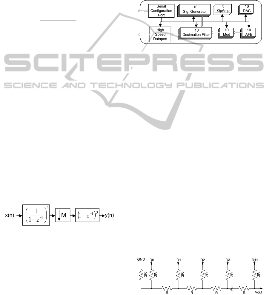
4.2 Decimation Filter
Decimation and low-pass filtering of the
modulator’s output signal is accomplished using a
comb filter having a sinc
3
(f) frequency response.
The implemented filter uses decomposition and
modulo arithmetic to minimize the system size
(Dijkstra et al., 1988). The decimation filters block
diagram is shown in Figure 3. The input signal x(n)
at oversampling frequency is first integrated by a 3
rd
order IIR filter. Next, decimation by a factor M is
carried out to obtain the final data rate. Finally, a 3
rd
order FIR differentiator generates the output of the
decimation filter.
Figure 3: Block diagram of the decimator.
5 DIGITAL SYSTEM CONTROL
AND INTERFACE
The communication to external components like a
DSP or FPGA is realized by two independent serial
ports. Therefore, the data and control paths are
strongly separated. Figure 4 shows an overview of
the signal and control flows. Serial configuration
port receives the control data and applies it to the
sub-blocks even for the high speed dataport, setting
up the data rate and the format of the transmission.
For testing purposes of the digital data transmission
the input of the decimator filters can be switched to
the on-chip signal generators. These generators are
based on the principle of digital resonators and are
capable of generating precise sine waves (Lu and
Roberts, 1994).
Figure 4: Digital system control and interface.
5.1 DC-suppression Feedback Circuit
Offset suppression of each electrode is realized by
an additional input of the AFE. If this feature is not
needed (e.g. for ECG application) this input can be
connected to the virtual ground node. For appli-
cations with very small amplitudes (e.g. EEG) the
electrode offset should be removed allowing the
required high amplification factor of the data path.
In this case, as shown in (1), the on-chip DACs are
used to generate the subtracting voltage.
The input of the DACs can be switched between a
value which is written into the configuration register
by the serial control port or the output of the on-chip
digital integrator. This integrator sums up the bit-
stream generated by the modulator and is config-
urable by the serial configuration port for different
time constants. To avoid noise of the high resistive
output node (100 kΩ) of the connected DAC and to
smooth the nonlinearities caused by value changing
of the DAC, a capacitor in the range between 1 µF
and 10 µF should be added between the V
DAC
output
and signal ground.
For the implementation of the DAC a R-2R
architecture (Allen and Holberg, 2002) was chosen
and is depicted in Figure 5, where the inputs D
0
-D
11
are connected to a 12-bit register. This DAC occu-
pies an area of 0.5 mm² and consumes only 33 µA.
Figure 5: R-2R architecture of implemented 12-bit DAC.
BIODEVICES 2011 - International Conference on Biomedical Electronics and Devices
40
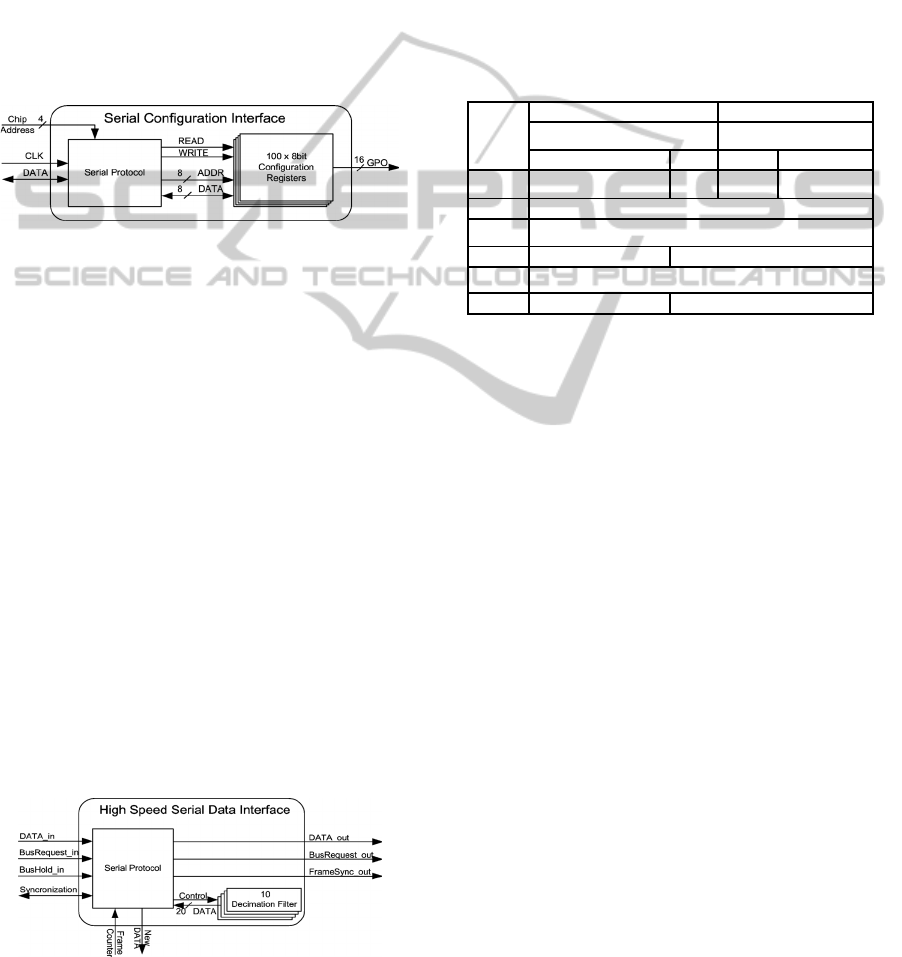
5.2 Serial Configuration Port
The serial communication for setting up the system
is realized by a synchronous bidirectional interface
and is shown in Figure 6. The access to one of the
hundred 8-bit registers is decoupled from other on-
chip components and can be done asynchronously to
the conversion clock and to the clock of the high
speed serial dataport. Depending on the external
interconnects the maximum bus speed can be used
up to 100 kHz. This allows continuously to set up
the DACs for offset cancellation and the external 16
General Purpose Outputs (GPOs) for controlling the
possible external components during operation.
Figure 6: Block diagram of the serial configuration port.
5.3 High Speed Serial Dataport
The data from the SoC are read out by the high
speed serial dataport which is synchronous to an
applied clock signal, Figure 7 shows its block dia-
gram. The receiver is synchronized to a new data
packet by the framesync signal. The rising edge of
this signal determines the new transmission, there-
fore, after a delay of one bit, the second bit is taken
as valid data. Busrequest and bushold signals
implement the handshake protocol allowing daisy
chaining of 16 SoCs, this number is determined by
the 4-bit chip address.
The serial data from one SoC includes a 22 x 16-
bit wide packet which is sent for each sampled value
of 10 channels. For a maximum data rate of 50k
packets per second a minimum clock transmission
frequency of 352 x 50k = 17.6 MHz is needed.
Hence, using the SoC in daisy chained application
the maximum operating frequency of this high speed
port is specified to 53 MHz to allow the data trans-
mission of 3 SoCs.
Figure 7: Block diagram of the high-speed serial dataport.
Table 3 shows the implemented protocol for one
data packet. The 1st word contains the start marker
FF9h and the chip address which is set by external
digital 4-bit port. The 2nd transmitted word is the
frame counter value. The 3rd word consists of the
upper 16-bit data of the first channel. The 4th data
word (bit 15..12) consists of the 4 lower data bits of
the first channel (channel <0>) and the actual DAC
value for the same channel. The following 18 words
are in the same scheme as for the first channel (3rd
and 4th words).
Table 3: Implemented protocol for the high speed
data-port.
16 bit
words
MSB LSB
nibble nibble
high low high low
Word1 Fh Fh 9h chip address
Word2 framecounter
Word3 upper 16 bits of ch. <0> data
Word4 lower 4 bits of data DAC value for ch. <0>
Word5 upper 16 bits of ch. <1> data
Word6 lower 4 bits of data DAC value for ch. <1>
6 RESULTS
A prototype of the SoC has been realized in a
0.35 µm CMOS process with a supply voltage of
3.3 V. To prevent coupling effects between digital
and analog blocks, care has been taken to separate
these parts in the layout. The power supply is
likewise separated; additional on-chip stabilizing-
capacitors are used for blocking off switching
activities on the supply rails. These capacitors,
which have been realized as poly-capacitors and
Metal-Insulator-Metal (MIM) capacitors, also allow
to fulfill the needed layer density specified by the
foundry. Additional efforts have been taken to
minimize resistive parasitics of the interconnects,
this applies in particular to the supply rails and the
connections to signal ground (V
SGND
).
A special approach was taken for the chopper
clock lines: To minimize coupling effects to the
analog parts due to high frequency switching
operation each chopper clock path has been placed
between two paths tied to ground.
A microphotograph of the fabricated SoC
prototype is shown in Figure 8. The SoC occupies an
area of 47 mm² and the number of pins is 144.
AN INTEGRATED MULTI-CHANNEL SYSTEM FOR BIOMEDICAL SIGNAL ACQUISITION
41
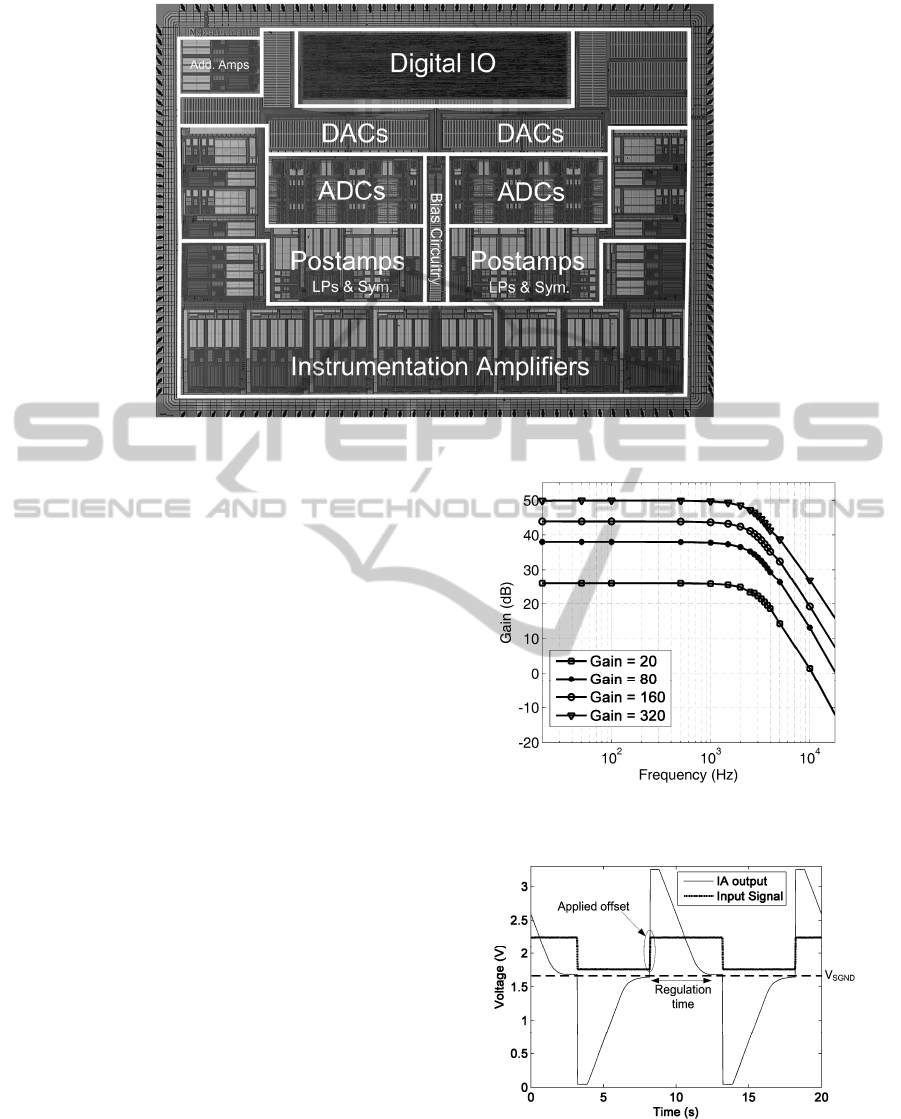
Figure 8: Microphotograph of the system-on-chip.
6.1 Analog Channel and CMRR
Calibration
The measured overall gains (20, 80, 160 and 320) of
analog channels for a bandwidth of 3 kHz are shown
in Figure 9, therein the external high-pass filter is
shorted and the DC-suppression is disabled. The
input referred offset of the channels (with enabled
chopper modulation) is less than 34 µV and 12 µV
for the low-power and low-noise mode, respectively.
The DC-suppression circuit has been tested by
applying a 500 mV
pp
square-wave to the input of the
IA. This signal and the output of the IA are shown in
Figure 10. The time constant of the on-chip digital
integrator has been set to approximately one second.
The IA saturates after the rising or falling edges of
the square wave. Due to regulation of the activated
DC-suppression, the offset voltage is subtracted
from the channel resulting in an offset free output at
signal ground (V
SGND
= 1.65 V).
The CMRR calibration of all 10 channels is shown
in Figure 11. The sweep of the implemented 64
calibration steps results in a channel CMRR of more
than the specified 80 dB at 50 Hz for at least one
calibration value.
Figure 9: Measured gain and bandwidth of an analog
channel. Markers indicate measured data points.
Figure 10: Example of the DC-suppression using a
square-wave input, the IA output settles back to signal
ground after the regulation time.
BIODEVICES 2011 - International Conference on Biomedical Electronics and Devices
42
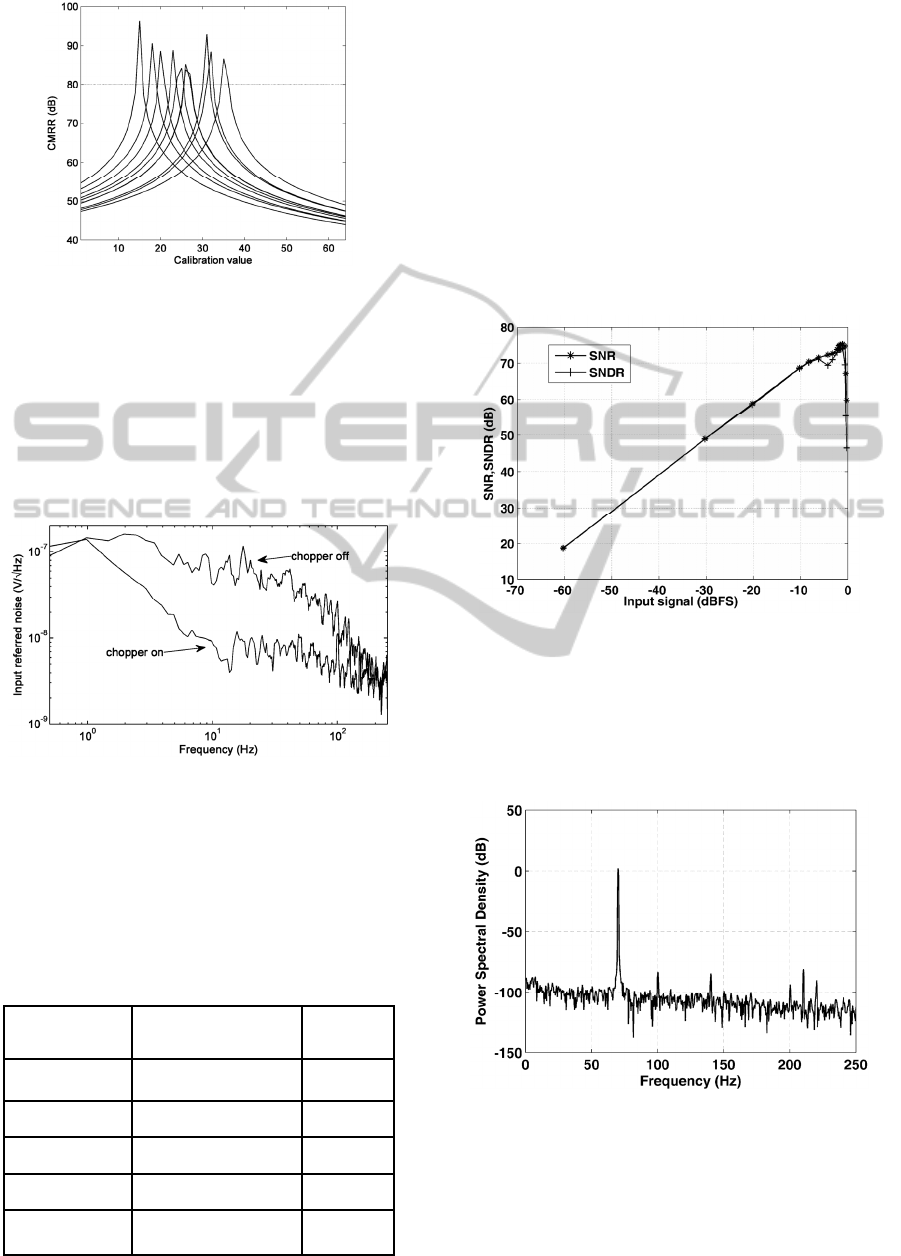
Figure 11: CMRR @ 50 Hz calibration of 10 channels.
6.2 Noise and Power
The total input referred noise has been measured
including the full channel, i.e. the AFE, ΣΔ-
modulator and decimation filter. Figure 12 shows
the influence of the chopper modulation for an ECG
application and Table 4 summarizes the noise
performance of the SoC.
Figure 12: Input referred noise density for ECG bandwidth
with chopper modulation on and off.
The power consumption of the SoC varies
between 28.7 mW in low-power mode and
209.8 mW in low-noise mode for data rates of
500 Hz and 50 kHz, respectively.
Table 4: Measured total input referred noise at ADC
output.
Integration
Bandwidth
(Signal Type)
Conditions/Remarks
Value
µVpp
0.05 Hz – 250 Hz
(ECG)
Low-power, chopper
enabled
1.13 – 1.74
Low-power, chopper
disabled
3.1 – 3.6
0.05 Hz – 70 Hz
(EEG)
Low-noise,
chopper enabled
< 0.68
0.01 Hz – 5 kHz
(EMG)
Low-noise,
chopper enabled
< 3.9
0.1 Hz – 3 kHz
(EP)
Low-noise,
chopper enabled
< 3.2
6.3 ADC
The ADC has been measured by applying a signal to
the input of the channel. Figure 13 displays the
measured signal to noise (SNR) and signal to noise
and distortion ratio (SNDR) versus input signal, and
Figure 14 the measured output spectrum for a 70 Hz
input signal with disabled chopper modulation for a
data rate of 500 Hz and OSR = 256.
The measured peak SNDR for this setup is 75 dB
which corresponds to an ENOB of 12.17 bits. An
ENOB of more than 15.2 bits has been measured for
the EEG bandwidth (0.05 Hz – 70 Hz ).
Figure 13: Measured SNR and SNDR versus input signal
for a 70 Hz sine input and ECG bandwidth of 250 Hz .
6.4 Digital IO
The digital communication ports are tested by the
setup shown in Figure 15. A C++ program running
Figure
14: Measured output spectrum for 70 Hz sine input
for the ECG bandwidth of 250 Hz.
on a PC communicates through the USB-interface
with a Field Programmable Gate Array (FPGA)
chip. The software loaded into the FPGA
AN INTEGRATED MULTI-CHANNEL SYSTEM FOR BIOMEDICAL SIGNAL ACQUISITION
43
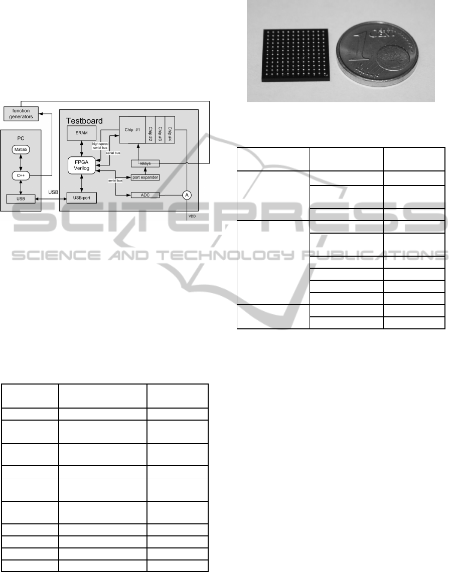
implements the protocols for both serial ports of the
SoC. The configuration port is tested by writing to
all 100 registers with subsequent read-out of the
written content and shows no missing data for a
communication frequency of up to 100 kHz. The
high speed serial bus was used for reading out of all
channel measurements presented in this section and
is operating properly for frequencies up to 55 MHz.
Figure
15: Test setup for the digital communication.
6.5 Summary
Using modern packaging technology the SoC is
encapsulated in a lead free Ball Grid Array (BGA)
having a size of 13 mm x 13 mm. Figure 16 shows a
size comparison of the packaged SoC to a eurocent
coin. The characteristics and a configuration
overview of the realized biomedical SoC are
summarized in Table 5 and 6, respectively.
Table 5: Main characteristics of the biomedical SoC.
Parameter Conditions/Remarks Value
Supply voltage 3.3 V
Current
consumption
Low-power – Low-noise 8.7 mA – 63.6
mA
Total input
referred noise
ECG
EEG
< 1.74 µVpp
< 0.88 µVpp
CMRR @ 50/60 Hz > 80 dB
Input common
mode range
V
El
= V
Ref
± 1 V
Offset comp.
range
High-pass & DC-
suppression
± 1 V
Crosstalk Between channels < - 60 dB
Die area 47 mm²
Pin number 144
Package size BGA 13 mm x 13 mm
Figure 16: Photo of the SoC in a BGA package.
Table 6: SoC configuration overview.
Functional Block
Parameter
Range/ Value
Timing
Master clock divider 1 - 8
Sample rate
reduction
1 - 256
Decimation rate 128 - 383
Analog Front-End
(AFE)
(adjustable per
channel)
Power down on / off
Gain 20 / 80 / 160 /
320
Bandwidth 3 kHz / 15 kHz
Chopper modulation on / off
Bias current × 1 - 16
CMRR calibration 64 steps
ADC (adjustable per
channel)
Bias current × 1 - 8
Data format signed / unsigned
7 DISCUSSION
AND CONCLUSIONS
An integrated ten channel biomedical signal
acquisition system-on-chip has been presented. Each
channel of the SoC includes an analog front-end that
is programmable with respect to noise and power
and an ΣΔ-analog-to-digital converter. In addition,
the system includes both a CMRR calibration and a
DC-suppression circuitry. The latter extends the
input-referred DC-suppression range to a remarkable
value of up to ± 1 V which largely exceeds the input
offset range of other integrated circuit solutions. The
SoCs digital interface is realized by means of a serial
configuration port and a high-speed data output port.
The implemented system-on-chip is not only
suitable for multi-electrode applications, where a
small system size is mandatory, but also for mobile
long-term biomedical signal acquisition.
For example:
• A 100 electrode EEG system can be realized on
a PCB area of less than 6 cm x 6 cm, consuming
only approx. 1000 mW.
BIODEVICES 2011 - International Conference on Biomedical Electronics and Devices
44

• A 9 channel ECG system would occupy only
few cm² and consuming less than 50 mW. This
would allow using only two standard AA batteries
for an application time of more than one week
(Galjan et al., 2008).
The presented SoC has been successfully employed
in experimental heart rate variability tests of resting
and stress test ECG recordings. At present,
biomedical signal recording systems that employ the
SoC are being developed and evaluated.
ACKNOWLEDGEMENTS
The authors would wish to acknowledge Natus
(formerly Schwarzer) Corporation, Munich, for their
support and very fruitful discussions. The authors
would also like to thank Sven Vogel for his
contributions to the design and Fabian Wagner for
support with the measurements.
REFERENCES
Martins, R., Selberherr, S., and Vaz, F. A., (1998). A
CMOS IC for portable EEG acquisition systems. IEEE
Trans. Instrum. Meas., 47(5), 1191-1196.
Ng, K. A., and Chan, P. K., (2005). A CMOS analog
front-end IC for portable EEG/ECG monitoring. IEEE
Trans. Circuits Syst. I, Reg. Papers, 52(11), 2335-
2346.
Yazicioglu, R. F., Merken, P., Puers, R., and Van Hoof,
C., (2007). 60 µW 60 nV/√Hz readout front-end for
portable biopotential acquisition systems. IEEE J.
Solid-State Circuits, 42(5), 1100-1110.
Desel, T., Reichel, T., Rudischhauser, S., and Hauer, H.,
(1996). A CMOS nine channel ECG measurement IC.
2nd International Conference ASIC.
Fuchs, B., Vogel, S., and Schroeder, D. (2002). Universal
application-specific integrated circuit for bioelectric
data acquisition. Medical Engineering and Physics 24,
695-701.
Martin, T., Jovanov, E., and Raskovic, D., (2000). Issues
in wearable computing for medical monitoring
applications: a case study of a wearable ECG
monitoring device. The Fourth International
Symposium on Wearable Computers, 43-49.
Galjan, W., Naydenova, D., Tomasik, J. M., Schroeder,
D., and Krautschneider, W. H., (2008). A portable
SoC-based ECG-system for 24h x 7d operating time.
In Proceedings of IEEE Biocas 2008, Baltimore, USA,
85-88.
Scheer, H. J., Sander, and T., Trahms, L., (2006). The
influence of amplifier, interface and biological noise
on signal quality in high-resolution EEG recordings.
Physiol. Meas., 27, 109-117.
Bronzino, J. D., (2000). The biomedical engineering
handbook. 2nd ed. CRC Press.
Webster, J. G., (1998). Medical instrumentation:
application and design. 3rd ed. Wiley & Sons, New
York.
Van Helleputte, N., Tomasik, J. M., Galjan, W., Mora-
Sanchez, A., Schroeder, D., Krautschneider, W. H.,
and Puers, R., (2008). A flexible system-on-chip
(SoC) for biomedical signal acquisition and
processing. Sens. Actuators A: Phys., vol. 142, Issue 1,
361-368.
Winter, B. B., and Webster, J. G., (1983). Driven-right-leg
circuit design. IEEE Trans. Biomed. Eng., 30, pp. 62-
66.
Bronskowski, C. and Schroeder, D. (2006). An ultra low-
noise operational amplifier with programmable noise-
power trade-off. In Proceedings 32nd ESSCIRC 2006,
Montreux, Switzerland, 368-371.
Allen, P. E, and Holberg, D. R., (2002). CMOS Analog
Circuit Design. Oxford University Press.
Maxim Integrated Products, (2000). Choosing the
optimum buffer / ADC combination for your
application. Application Note 1094.
Medeiro, F., Pérez-Verdú, B., de la Rosa, J. M., and
Rodríguez-Vázquez, Á., (1997). Using CAD Tools for
Shortening the Design Cycle of High-Performance
ΣDM: A 16.4bit 9.6 kHz 1.71mW ΣDM in CMOS
0.7µm Technology. International Journal of Circuit
Theory and Applications, 25, 319-334.
Fuchs, B. (2004). Integrierte Sensorschaltungen zur EKG-
und EEG-Ableitung mit prädiktiver Signalver-
arbeitung. PhD thesis, Institute of Nanoelectronics,
Hamburg University of Technology, Shaker Verlag,
Aachen.
Dijkstra, E., Nys, O., Piguet, C., and Degrauwe, M.,
(1988). On the use of modulo arithmetic comb filters
in sigma delta modulators. In IEEE Proc. ICASSP88,
2001-2004.
Lu, A., and Roberts, G., (1994). A high-quality analog
oscillator using oversampling D/A conversion
techniques. IEEE Trans. Circuits Syst. II Analog Digit.
Signal Process. 41 (7), 437–444.
AN INTEGRATED MULTI-CHANNEL SYSTEM FOR BIOMEDICAL SIGNAL ACQUISITION
45
