
INTRODUCING A NEW HALL EFFECT SENSOR
Novel Dynamic Offset Reduction Method
Vlassis N. Petoussis, Panos Dimitropoulos, George Stamoulis and Elias Houstis
University of Thessaly, Department of Computer & Communication Engineering
37th Glavani & 28th October Str., Volos, Greece
Keywords: Hall effect sensor, Offset reduction.
Abstract: Silicon Hall plates show an offset of a few millitesla. A large portion of this offset is caused by mechanical
stress in the device. The offset can be reduced when the spinning - current principle is applied. In this paper
we present a model and numerical analysis of a new Hall effect sensor which using a novel offset reduction
method. We call it “Wheel Hall Senor” and senses all 3 filed dimensions. The flux-density of B
Z
is
proportional to the DC component of the output signal, whereas the B
X
and B
Y
components are proportional
to the first harmonic of the output signal. Furthermore we calculate the function which governs the changes
in the electric field inside the new Hall effect sensor in presence of magnetic field. This function help us to
control in MatLab environment the equipotential lines and to monitor the changes in biasing conditions.
About the new sensor, the combination of his pioneering form and the elaborate sequence of using the
dynamic spinning current technique, could be lead to satisfactory results of produced Hall voltage with
small noise in a presence of external magnetic field.
1 INTRODUCTION
Hall plates are used in a wide variety of applications
to measure static and dynamic magnetic fields. A
major drawback of these sensors is their high offset
voltage, i.e., an output signal in the absence of a
magnetic induction. According to (A. Bellekom,
1994) the effects which contribute to the offset
voltage are piezoresistive effects, geometrical errors,
temperature gradients, nonhomogeneities, etc.
However, the offset voltage with a spatially periodic
nature differs from the Hall voltage, which is
constant. One way to reduce the offset caused by
orthogonal asymmetries is to use coupled symmetric
Hall plates (Maupin, 1980). However, the offset can
never be completely cancelled because there will
always be small differences between the Hall
devices. To overcome the mismatch, the bias current
of a single four contact Hall device is spun by
contact commutating and the resulting output
voltages are averaged over time. The orientation
dependence of the offset sources in silicon suggests
that orthogonal switching is not sufficient. To cancel
components of higher asymmetries a multicontact
Hall plate with more than four terminals is
necessary. The method presented in this paper is
based on Hall device with sixteen outside and
sixteen inside contacts. The spinning current vector
is generated by two harmonic biasing currents. As a
result, the output signal becomes spatially
continuously accessible, hence, asymmetries of
higher order can be cancelled out. Aim of present
work is the presentation of new Hall sensor with
pioneering form that reminds cogwheel with two
lines teeth, one internally and one externally (for this
reason we name it “Wheel Hall Sensor”) but also
with different way in the cancellation of offset
voltage and finally 1/f noise rejection. Initially the
designing constituted fundamental objective that as
aim had the respect and compatibility in the existing
techniques of reduction 1/f noise and also offset
voltage. For this aim was selected the circular
structure.
2 OFFSET VOLTAGE
In a standard IC process Hall plates have the
advantage of cheap and small. Therefore they are
quite often used in applications where the permanent
magnet is combined with the sensor. Because Hall
plates show a large offset the magnet used in these
464
Petoussis V., Dimitropoulos P., Stamoulis G. and Houstis E..
INTRODUCING A NEW HALL EFFECT SENSOR - Novel Dynamic Offset Reduction Method.
DOI: 10.5220/0003397304640469
In Proceedings of the 1st International Conference on Pervasive and Embedded Computing and Communication Systems (PECCS-2011), pages
464-469
ISBN: 978-989-8425-48-5
Copyright
c
2011 SCITEPRESS (Science and Technology Publications, Lda.)
applications have to be a strong magnet. The offset
of the Hall plate is the voltage that is measured when
no magnetic field is applied. Eq.1 represents the
theoretical situation, when an offset is added this
equation becomes:
offsetH
VISBV
(1)
Where I is the biasing current and S is the current –
related sensitivity. To reduce the offset, which is
time variant, spinning current Hall plates was
developed (Popovic, 1991). These are symmetrical
Hall plates with more than 4 contacts. In this multi
contact Hall plates the bias current is switched in for
example, eight directions through the Hall plate and
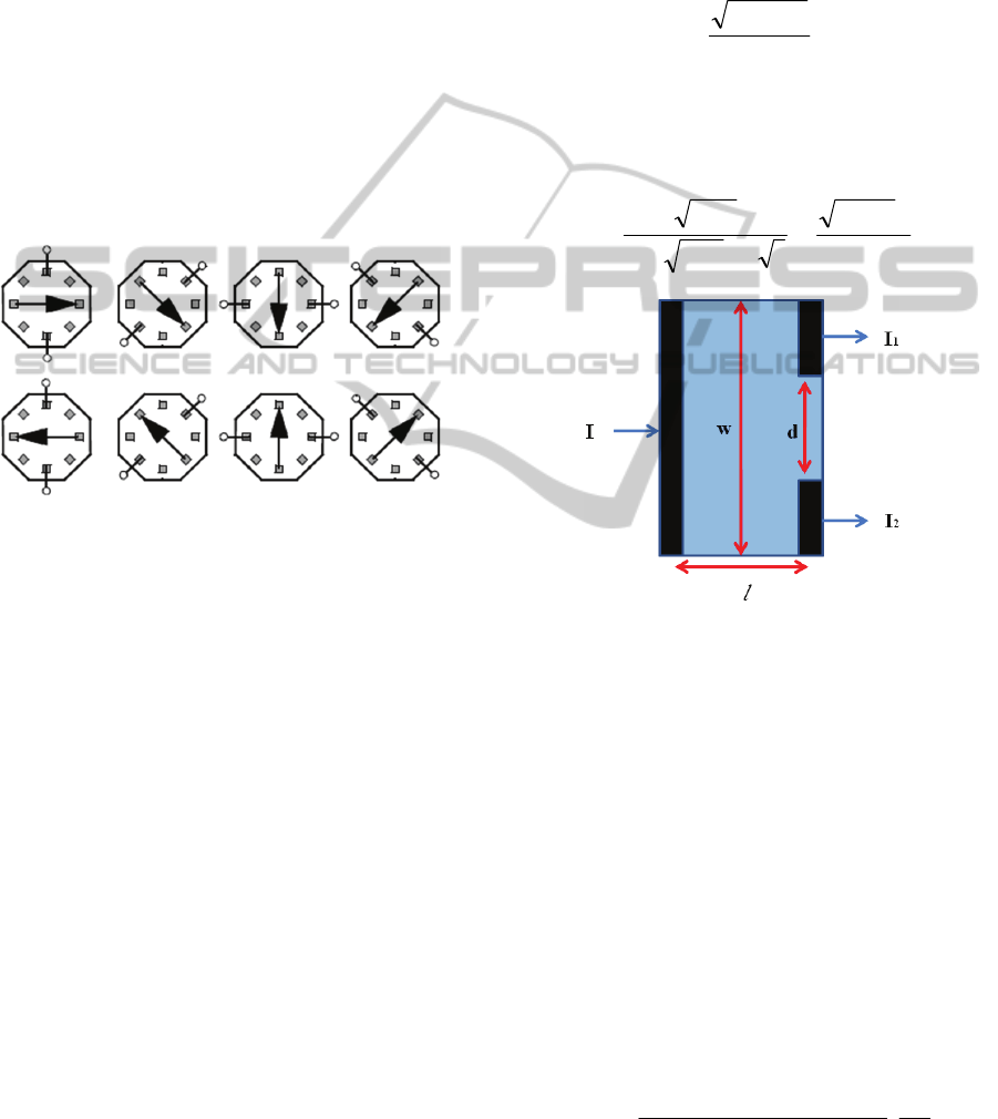
the corresponding voltages are measured, see Fig
1.(S.Bellekom, 1997).
Figure 1: An eight contact spinning-current Hall plate with
the possible bias current directions.
The measured voltages represent one period of a
(radial spatial) periodic signal. The spinning current
method uses this periodicity, it separates
transduction effects according to their spatial radial
periodicity. The Hall effect itself does not depend on
bias current direction and is therefore present in the
DC component. So, a spinning-current Hall plate
solves one of the most important drawbacks in
integrated silicon Hall plates, their offset.
3 THE
SPLIT – CURRENT MODEL
In this section, we will represent the magnetic field
resolution achievable with Hall split-current, sensor
and the offset voltage for a Hall plate. The presented
results have been checked modeling the Hall devices
with an equivalent electrical circuit, consisting of a
network of resistances and voltage controlled current
sources, as proposed in (Maier, 1999, Popovic,
1985). Fig. 2 shows the structure of a split-current
device, placed in a static magnetic field B=
z
B
ˆ
, and
biased with a current I. The current difference
between the two split contacts is (Popovic, 1991):
IBFI
(2)
where l and w are the length and width of the device,
d is the distance between the split contacts, and F is
a magneto-geometrical factor Thus:
BI
RkT
B
/
/4
min
(3)
F is the maximum for l/w 1, d/w 1, and μB<<1.
In these conditions, F
1. Optimum magnetic field
resolution for a given area is obtained for l w and
μB<<1, where:
w
kTR
twen
kT
B
sat
sat
opt
0
min,
44
(4)
Figure 2: The split-current Hall Effect Device.
4 THE CHANGES IN THE
ELECTRIC FIELD INSIDE THE
SENSOR
In this section we calculate a set of functions which
governs the changes in the electric field inside the
new Hall effect sensor in presence of magnetic field
B. This function help us to control in MatLab
environment the equipotential lines and to monitor
the changes on them when biasing conditions are
change. In our split-current model we use Dirichlet
and Neumann boundary conditions as we can see in
Fig.3. Use the following empirical expressions
(Vinal, 1982):
2
16 3 0.72
1265
(65.0 )
1[ /(8.510 )]
n
T
cm
Nxcm Vs
(5)
INTRODUCING A NEW HALL EFFECT SENSOR - Novel Dynamic Offset Reduction Method
465
2
16 3 0.72
447.3
(46.7 )
1[ /(6.310 )]
p
T
cm
Nxcm Vs
(6)
where N
T
denotes the total ionized impurity
concentration. For the Hall mobility we use the
approximation (Smith, 1978), μ* = rμ, with
r = <τ
2
>/<τ>
2
(Vinal, 1982). We consider
semiconductor slabs of rectangular geometry with a
magnetic field perpendicular to the device surface: B
= (0, 0, B,). The distributions of carriers and the
potential in the device depend only on x and y and
we solve a two-dimensional problem.
2
()
1( )
p
p
B
cB
x
B
2
()
1( )
n
n
B
cB
x
B
(7)
where:
y
J
Bc
pB
ˆ
)(
And we get two equations (Eq.7) for a p and n type
respectively. These equations give us the
dependence of the electric field inside the sensor in
presence of magnetic field.
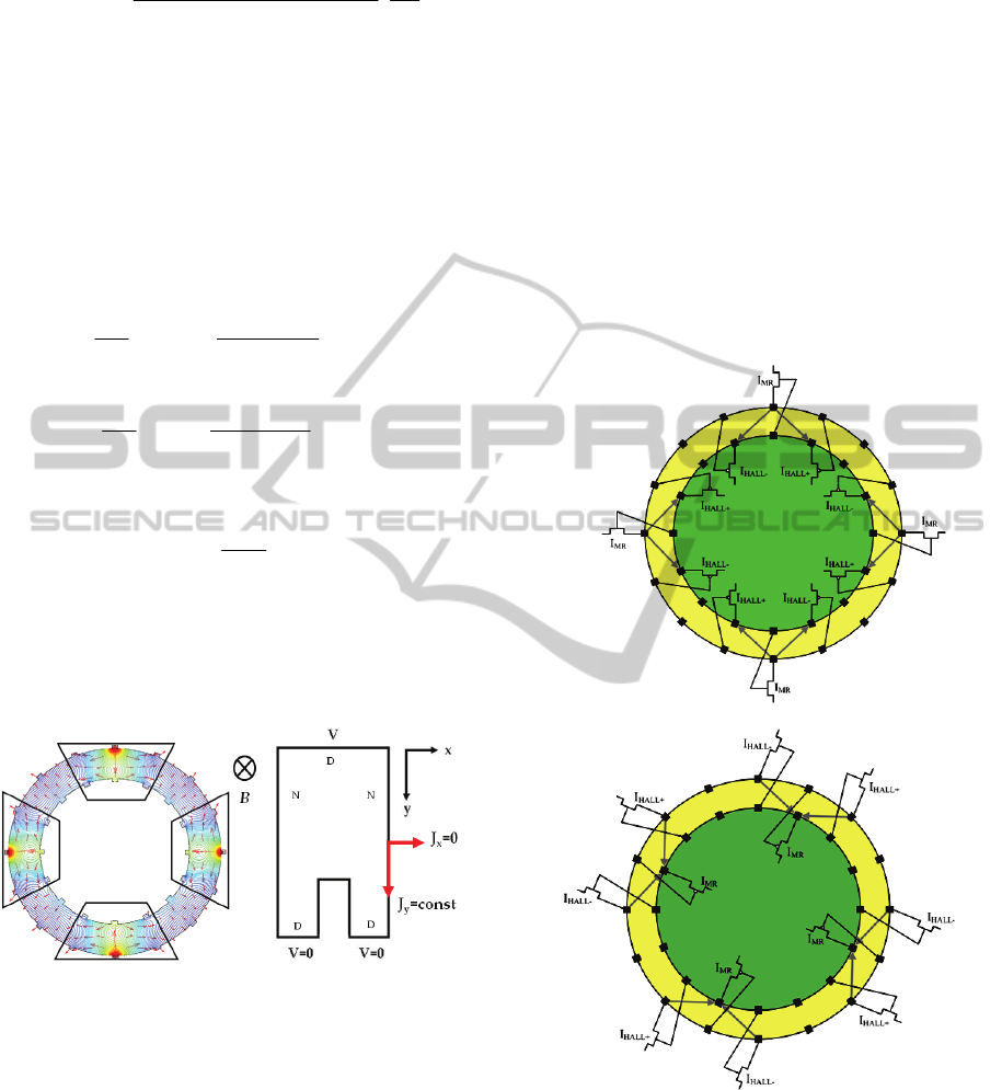
(a) (b)
Figure 3: The boundary conditions for a split-current
element Hall effect device. a) The area of the received
Hall voltage tacked in four places of the sensor. We can
see that the margins of the field in our model is well
separated each other (black trapezoid areas). b) Graphic
representation of a simple model in even phase, with D
and N presented the boundary conditions. Dirichlet
boundary conditions in contacts with positive or zero
potential and Neumann boundary conditions elsewhere.
5 THE WHEEL HALL SENSOR
A novel Hall sensor device introduced which uses
elaborate spinning current technique. The novel Hall
device that we call “Wheel Hall Senor” is presented
in Figures 4a and 4b. The current enters the device,
as presented in the aforementioned Figures, in two
phases namely the even phase (PHASE-P) and the
odd phase (PHASE-N). The device exploits the
signals attributed to Hall voltage, Hall current and
geometric MR effect. As a result the device is
equivalent to an “ideal” voltage or current Hall
sensor with geometrical factor of one (G
H
= 1 or
F = 1). Moreover it provides for high-speed
spinning, given that the voltage distribution changes
moderately between different phases. This is
equivalent to minimum charge injection that 0 in
turn – allows spinning frequency increase.
(a)
(b)
Figure 4: The novel Hall device that we call “Wheel Hall
Senor” or WHS. (a) The even phase (PHASE-P); (b) the
odd phase (PHASE-N).
Rotating in the clock wise direction we changing
periodically between the two phases and we are able
to have in each phase simultaneously 0
0
and 90
0
degree representation (as in spinning current
technique) of the Hall voltage. Due to the periodicity
PECCS 2011 - International Conference on Pervasive and Embedded Computing and Communication Systems
466
of the piezoresistive constants in the chip plane the
sensor’s offset is inverted if the current is switched .
When averaged, the offset-related part of the signal
is suppressed, whereas the component related to the
magnetic field remains unchanged. Single-sensor
applications have been implemented also in the past
with 2, 8, and 16 current directions (Munter. 1990,
Gottfried. 1991, Biolotti, 1997).
6 THE OFFSET REDUCTION
METHOD
To reduce the offset, the new Hall effect sensor uses
spinning-current technique in the symmetrical Hall
plate (Fig.4). In the offset reduction sequence the
direction of the bias current is splited right and left
and the corresponding output voltage is measured on
the contacts in
45
0
to the current direction in each
phase. The total number of measurements at each
phase is in four places like a cross and all phases
give as the total Hall voltage. When sixteen outside
and sixteen inside contacts are used, the bias current
is switched
45
0
for each measurement, the voltage
contacts are switched outside to inside respectively
(Fig. 5). For each phase of the bias current, four
output (V
H+
and V
H-
) and input (V
H-
and V
H+
)
voltages are measured in a rotating clock wise.
(a)
(b)
Figure 5: The even phases (a) and the odd phases (b). With
I we denote the current bias in 45
0
direction in each
measurement and V
H+
and V
H-
denoted the two Hall
Voltage references in each phase (for n-type material).
Finally for each turn in PHASE-P and PHASE-
N, totally sixteen Hall voltages are measured. Each
harmonic biasing current in each phase produces an
offset voltage witch totally in turns gives us the
offset cancellation. So offset caused from current I
AD
in phase P cancel the offset caused from current I
CD
in phase N and I
AD
in phase N cancel the offset
caused from current I
AF
in phase P. Finally the one
offset in one phase cancel the other in next phase
(Petoussis, 2009).
7 THE REAL STRUCTURE
OF THE SENSOR
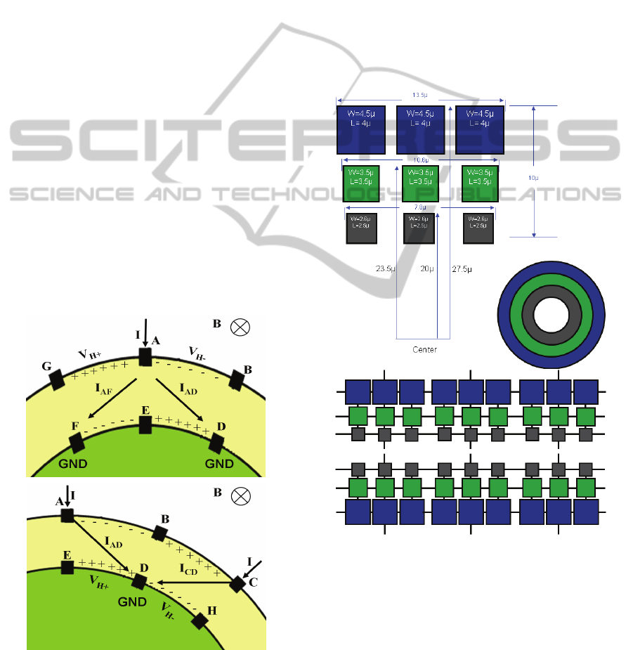
Figure 6: The real structure of the “Wheel Hall Sensor”.
A triple group of p-n junction diffusion with proposed
dimensions. We see only a part of the 144 p-n junction
diffusions divided in triple groups, each group has a
contact for measuring and biasing.
The main shape of the sensor is a circle (Fig.4). This
shape to be in real material contains problems
especially on the offset caused by stress.
Furthermore the designed shape must satisfy a way
to be easy functionally for a spinning-current
INTRODUCING A NEW HALL EFFECT SENSOR - Novel Dynamic Offset Reduction Method
467

technique. The final decision was to develop the
sensor in a row with a two lines of small Hall Effect
devices with up and down parts in a reversed
trapezoid shape resemble the real cycled structure of
the sensor. We need totally 144 p-n junction
diffusions pieces (Fig.6) divided in 32 triple
trapezoid groups, each group has a contact for
measuring or biasing and finally we use 32 contacts.
8 FIELD SIMULATIONS
In this part we present simulations of the device
structure with a MatLab simulator. The main goal
was to see the behavior of the electric field inside
the device when this exposed in external magnetic
field Fig (7a, 7b). In a way to control the
equipotential lines in it, we solve the Laplace
equation using the boundary conditions that we saw
in the split current model previously. The results
show us that the shape and the place of the contacts
is in the right position and are well combined in
even and odd phase during the spinning current
technique.
(a)
(b)
Figure 7: The novel Hall device that we call “Wheel Hall
Senor” or WHS. (a) The electric field and the equpotential
lines in the even phase (PHASE-P) for B
0; (b) The
electric field and the equpotential lines in the odd phase
(PHASE-N) for B
0.
9 CONCLUSIONS
In this paper we analyze the theoretical and the
technical way of the structure of a new Hall Effect
Sensor which uses an elaborate spinning current
technique. Using as shape with a row of a two lines
of small Hall Effect devices with up and down parts
we are able to reduce the stress offset and we able to
support reduced the 1/f noise measurements using
fast spinning current technique. Moreover it
provides for high-speed spinning, given that the
voltage distribution changes moderately between
different phases. This is equivalent to minimum
charge injection that 0 in turn – allows spinning
frequency increase. The device senses all 3 filed
dimensions, namely the flux-density of B
Z
is
proportional to the DC component of the output
signal, whereas the B
X
and B
Y
components are
proportional to the first harmonic of the output
signal. Finally the device can be made in a way to
reuse the current, if integrated in a BiCMOS
technology providing for matched JFETs.
ACKNOWLEDGEMENTS
I would like to thank Pr. Dr. George Stamoulis, Dr.
Panos Dimitropoulos for the useful advices and Pr.
Dr. Manolis Vavalis for the helpful discussions.
furthermore I would like to thank the electrical
engineering & computer engineering department of
the university of thessaly for the technical support
and fulfillment of this work.
REFERENCES
A. A. Bellekom and P. J. A. Munter, “Offset reduction in
spinning current Hall plates,” Sensor and Materials
5,253- 263, 1994.
J. Maupin and M. Geske, ”The Hall effect in silicon
circuits,” The Hall effect and its applications, ed. C.
Chien and C. Westgate, New York, 1980.
R. S. Popovic, Hall Effect Devices, Adam Hilger, Bristol,
1991.
Sandra Bellekom, Lina Sarro. International Conference on
Solid-State Sensors and Actuators, Chicago, June 16-
19, 1997 p.233-p236.
C. Maier, M. Emmenegger, S. Taschini, H. Baltes, J. G.
Korvink, Equivalent circuit model of resistive IC
sensors with the box integration method, IEEE Trans.
Comput.-Aided Des. Integr. Circuits Syst. 18 (1999)
1000–1013.
R. S. Popovic, Numerical analysis of MOS magnetic field
sensors, Solid State Electron. 28 (1985) 711–716.
PECCS 2011 - International Conference on Pervasive and Embedded Computing and Communication Systems
468

P. J. A. Munter, “A low-offset spinning-current hall
plate,” Sensors Actuators A, vol. 21–23, pp. 734–746,
1990.
R. Gottfried and G. Zimmer, “CMOS-compatible
magnetic field sensors fabricated in standard and in
silicon insulator technologies”, Sensors Actuators, vol.
A27, pp. 753–757, 1991.
A. Biolotti, G. Monreal, and R. Vig, “Monolithic magnetic
hall sensor using dynamic quadrature offset
cancellation sensors,” IEEE J. Solid- State Circuits,
vol. 32, pp. 829–836, June 1997.
A. W. Vinal and N. A. Masnari, “Magnetic transistor
behav:cslr explained by modulation of emitter
injection, not carrier deflection,” IEEE Electron
Device Lett., vol. EDL-3, pp. 203-2C 5,1982.
A. W. Smith, Semiconductors. New York: Cambridge,
1978.
A. W. Vinal and N. A. Masnari, ‘Response to “Comment
on ‘Magnetic transistor behavior explained by
modulation of emitter injection, not carrier deflection,’
IEEE Electron Device Lett., vol.EDL ,pp. 396-397,
1982.
Vlassis N. Petoussis. P. Dimitropoulos, George Stamoulis,
A Novel Hall Effect Sensor Using Elaborate Offset
Cancellation Method, Sensors & Transducers Journal,
Vol. 100, January 2009, pp. 85-91.
INTRODUCING A NEW HALL EFFECT SENSOR - Novel Dynamic Offset Reduction Method
469
