
PHOTONIC ANALOGUE-TO-DIGITAL CONVERTER BASED ON
WAVELENGTH DIVISION MULTIPLEXING TECHNIQUE
Tiago Alves and Adolfo Cartaxo
Group of Research on Optical Fibre Telecommunication Systems, Instituto de Telecomunicac¸˜oes, DEEC
Instituto Superior T´ecnico, Av. Rovisco Pais 1, 1049-001, Lisboa, Portugal
Keywords:
Photonic analogue-to-digital converter, Time stretching, Ultra wideband, Wavelength division multiplexing.
Abstract:
A photonic (Ph) analogue-to-digital (ADC) converter architecture based on the wavelength division multiplex-
ing (WDM) technique used to provide compressed spectrum of the ultra wideband radio signals that are being
used in a given pico-cell area for monitoring purposes is presented. The signal at the different points of the
WDM Ph-ADC architecture is analyzed and discussed in detail. The advantages/disadvantages of the WDM
architecture are identified and compared with its time division multiplexing (TDM) counterpart.
It is shown that the WDM Ph-ADC architecture provides adequate time stretching of the wireless signals
captured in a given pico-cell. This system enables relaxing the bandwidth requirements of the electrical ADCs
used to digitize the wireless signals prior digital signal processing is applied for spectrum and transceivers
localization monitoring. In addition, it is concluded that the WDM Ph-ADC architecture supports higher
pulse repetition rates than the TDM Ph-ADC architecture being of special interest when a fast up-date of the
radio channel monitoring is required.
1 INTRODUCTION
The photonic (Ph) analogue-to-digital converter
(ADC) system was initially proposed as a pow-
erful solution to provide time-stretching/frequency-
compression of high frequency signals in order to re-
lax the electrical receivers bandwidth (Han and Jalali,
2003).
Recently, a multi-channel Ph-ADC system based
on time division multiplexing (TDM) technique has
been proposed (Llorente et al., 2008; Llorente et al.,
2009; Alves and Cartaxo, 2011). This Ph-ADC
system is used to compress the spectrum of ultra-
wideband (UWB) radio signals captured from sen-
sor antennas that are strategically located inside home
premises. From this compression, spectrum moni-
toring, fingerprinting and localization of the different
UWB transceivers that are being used in a given pico-
cell can be performed by digital signal processing
(DSP) techniques. The main advantage of such Ph-
ADC system is the relaxed requirements of the elec-
tronic ADCs (E-ADC) used to monitoring the whole
UWB band (from 3.1 until 10.6 GHz). In this paper, a
Ph-ADC based on the wavelength division multiplex-
ing (WDM) technique is proposed for the first time
(to the best of our knowledge). The operational lim-
its of the WDM Ph-ADC architecture are analyzed
through numerical simulation and discussed in detail.
The main advantages/disadvantages of this architec-
ture when compared with the TDM-based architec-
ture are also identified.
2 WDM PH-ADC
ARCHITECTURE
2.1 System Description
Fig. 1 depicts the setup diagram of the WDM Ph-
ADC architecture. The optical source may be im-
plemented using a super continuum (SC) source gen-
erating an optical pulsed signal with a flat wideband
spectrum. This spectrum is then filtered (for instance,
using an arrayed waveguide grating (AWG)) in sev-
eral slices (as much as the number of sensors used
to acquire the electrical signals from the radio in-
terface in a given room scenario), multiplexed and
launched into a dispersive spool of fibre in order to
stretch the time signal waveforms. After the fibre,
111
Alves T. and Cartaxo A..
PHOTONIC ANALOGUE-TO-DIGITAL CONVERTER BASED ON WAVELENGTH DIVISION MULTIPLEXING TECHNIQUE.
DOI: 10.5220/0003551501110120
In Proceedings of the International Conference on Data Communication Networking and Optical Communication System (OPTICS-2011), pages
111-120
ISBN: 978-989-8425-69-0
Copyright
c
2011 SCITEPRESS (Science and Technology Publications, Lda.)
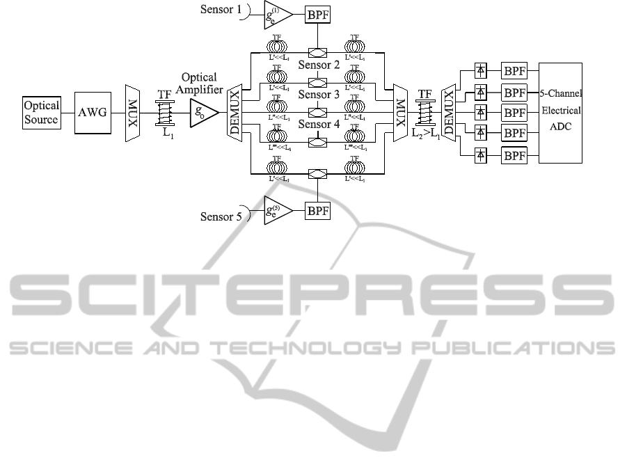
Figure 1: Schematic diagram of the photonic part of the WDM Ph-ADC architecture.
the different optical pulsed signals (each one centred
at a different optical wavelength) are demultiplexed
and used to feed each electro-optic modulator (EOM)
that is located in each sensor antenna. The wire-
less signals acquired in each sensor antenna are then
used to modulate the respective optical pulsed signal.
It should be highlighted that, with this architecture,
the electrical signal snapshots acquired by the differ-
ent sensors antennas in a given time instant are con-
verted to the optical domain at the same time instant
(apart the walk-off between the different wavelengths
resulting from the propagation along the first spool
of fibre) using optical pulsed signals transmitted at
different wavelengths. Instead, in the TDM archi-
tecture, only one wavelength is used and the snap-
shots of the different sensors are transmitted sepa-
rately in time. The optical pulsed signals are then
multiplexed and launched into the second spool of fi-
bre. After achieving the proper time stretching (TS)
by adequate adjustment of the dispersion of the first
and second spool of fibres, the optical signals car-
ried in the different wavelengths are demultiplexed
and the electrical signals snapshots are obtained us-
ing positive-intrinsic-negative (PIN) photo-detectors.
The detected electrical signals are band-pass filtered
(to reduce the low frequency/high power spectrum
due to the optical pulsed signal) and applied to the
E-ADC card where DSP is accomplished. From the
comparison of the WDM with the TDM Ph-ADC ar-
chitecture presented in (Alves and Cartaxo, 2011), the
following outcomes are drawn: a wider band optical
source is required in the WDM than in the TDM ar-
chitecture; ii) the WDM architecture may be more ex-
pensive than the TDM as it requires additional op-
tical devices as multiplexers (MUXs), demultiplex-
ers (DEMUXs) and PIN photo-detectors, and electri-
cal devices as band-pass filters (BPFs) and electrical
amplifiers and iii) the WDM architecture requires a
multi-channel E-ADC card as the signals may arrive
to the card simultaneously. The main advantage of
the WDM architecture over the TDM one is related
to the possibility of having a higher pulse frequency
rate that enables faster up-dating on the fingerprint-
ing, localization and power levels control of the UWB
transceivers used in a given pico-cell.
2.2 Description of the WDM Ph-ADC
System Parameters
The analysis of the WDM Ph-ADC architecture is
accomplished considering similar parameters to the
ones used in (Alves and Cartaxo, 2011) for the TDM
Ph-ADC architecture. Particularly, it is considered
that:
• The arrayed waveguidegrating is characterized by
a Gaussian transfer function (in order to have op-
tical time pulsed signals with a Gaussian shape)
with a -3 dB bandwidth of 1.7 nm.
• The time stretching factor is 3.4 (and conse-
quently the fibre spools lengths are the same as
for the TDM solution) in order to meet the time
aperture specifications mentioned in (Alves and
Cartaxo, 2011).
• The electro-optic conversionis performed by con-
ventional Mach-Zehnder modulator biased at the
quadrature point.
• The electrical and optical amplifiers present the
same noise characteristics to the ones considered
in (Alves and Cartaxo, 2011).
• A 6-th order band-pass Bessel filter with a -3 dB
bandwidth of 13 GHz and with maximum ampli-
tude response at 5.48 GHz is used in each sensor
to model the limited bandwidth of the electrical
noise and a 6-th order band-pass Bessel filter with
OPTICS 2011 - International Conference on Optical Communication Systems
112
20 25 30 35 40
0
0.2
0.4
0.6
0.8
1
t [ns]
Normalized Intensity
B
−3dB
= 300GHz
(a)
20 25 30 35 40
0
0.2
0.4
0.6
0.8
1
t [ns]
Normalized Intensity
B
−3dB
=400GHz
(b)
20 25 30 35 40
0
0.2
0.4
0.6
0.8
1
t [ns]
Normalized Intensity
B
−3dB
=500GHz
(c)
Figure 2: Normalized intensity of the optical pulses at the DEMUX input (continuous line) and the DEMUX output (dashed
line).
a -3 dB bandwidth of 1.4 GHz and with maximum
amplitude response at 1.1 GHz is used at the PIN
output.
• The transmission over the first and second spools
of fibre is linear.
However, the pulse repetition rate used in the
WDM architecture is five times higher than the one
used in the TDM architecture presented in (Alves and
Cartaxo, 2011) - 3.23 MHz - as the optical pulses are
not multiplexed in time.
3 WDM PH-ADC
ARCHITECTURE OPERATION
IN THE ABSENCE OF
ELECTRICAL SIGNALS
The appropriate operation of the WDM Ph-ADC ar-
chitecture is limited mainly by two parameters: the
optical channel spacing used between the different
optical transmitted channels and the bandwidth of the
MUXs/DEMUXs used to combine/separate those op-
tical channels. In this section, a brief study on the
impact of these parameters on the WDM Ph-ADC ar-
chitecture is accomplished. To simplify the analysis,
no electrical signals applied to the EOM are consid-
ered.
3.1 Bandwidth of MUXs/DEMUXs
In this work, the absence of (or negligible) time wave-
form differences between the signals before and af-
ter the MUXs/DEMUXs operation is considered as
a criterion to identify the most adequate bandwidth
for these devices. This criterion is used in order to
obtain low distortion induced by the 2 MUXs and 2
DEMUXs chain of the WDM Ph-ADC system on the
time waveform. The study is accomplished by taking
into account the WDM Ph-ADC system described in
section 2 and considering the transmission of only one
optical pulsed signal (obtained by proper filtering of
the flat spectrum generated by the SC source) in order
to avoid inter-channel crosstalk.
Fig. 2 shows the normalized intensity of one opti-
cal pulse at the DEMUX (located after the first spool
of fibre) input and output for different -3 dB band-
width values of the DEMUX Gaussian shape. Fig. 2
shows that tight bandwidths decrease the time aper-
ture of the optical pulse. It is also shown that al-
though the optical pulse remains almost unchanged
for a bandwidth of 500 GHz, the reduction of the
pulse time aperture cannot be neglected anymore for
a bandwidth of 300 GHz. For the 400 GHz bandwidth
case, a slight reduction of the time aperture is also ob-
served. Nevertheless, this reduction is not much sig-
nificant and the 400 GHz bandwidth case is preferable
(when compared with 500 GHz) as it allows for lower
optical channel spacing in the WDM architecture and,
consequently, for lower optical bandwidth require-
ments in the WDM Ph-ADC system. Hence, in this
work, the -3 dB bandwidth of the MUXs/DEMUXs
used along the optical path is set to 400 GHz.
3.2 Optical Channel Spacing
Due to the very large bandwidth of each optical sig-
nal used to ”sample” the radio signals captured by the
sensors antennas, the walk-off induced by the fibre
on each WDM channel may be of special relevance
and its impact on the system operation should be care-
fully analyzed. The study of the influence of the op-
tical channel spacing on the WDM operation is ac-
complished by considering the Ph-ADC architecture
comprising five sensors as depicted in Fig. 1.
Fig. 3 depicts the time waveform and the power
spectral density (PSD) of the multiplexed signal at the
output of the first spool of fibre considering an opti-
cal channel spacing of 600 GHz. Fig. 3(b) shows a
PHOTONIC ANALOGUE-TO-DIGITAL CONVERTER BASED ON WAVELENGTH DIVISION MULTIPLEXING
TECHNIQUE
113
0 0.2 0.4 0.6 0.8 1 1.2 1.4
0
0.2
0.4
0.6
0.8
1
t [µs]
Normalized Intensity
(a)
0 0.01 0.02 0.03 0.04 0.05 0.06
0
0.2
0.4
0.6
0.8
1
t [µs]
Normalized Intensity
(b)
−2 −1 0 1 2
−40
−20
0
20
40
ν−ν
0
[THz]
Normalized PSD
(c)
Figure 3: a) Multiplexed optical pulses at the output of the
first spool of fibre. b) Zoom of a). c) PSD of the mul-
tiplexed signal represented in a). Results obtained for an
optical channel spacing of 600 GHz.
zoom of the WDM signal in the time domain. The
five pulses presented in Fig. 3(b) are the optical pulses
corresponding to each one of the five optical channels
used in the WDM Ph-ADC architecture (see the sig-
nal spectrum in Fig. 3(c)). They appear separated in
time due to the walk-off effect occurred along the first
spool of fibre. As the WDM signal is still launched
into the second spool of fibre, the impact of the walk-
off on the relative delay between the optical channels
is still further increased.
Fig. 4(a) depicts the time waveform correspond-
ing to the WDM signal at the output of the second sp-
0 0.2 0.4 0.6 0.8 1 1.2 1.4
0
0.2
0.4
0.6
0.8
1
t [µs]
Normalized Intensity
(a)
0 0.05 0.1 0.15 0.2
0
0.2
0.4
0.6
0.8
1
t [µs]
Normalized Intensity
(b)
Figure 4: a) Multiplexed optical pulses at the output of the
second spool of fibre. b) Zoom of a). Results obtained for
an optical channel spacing of 600 GHz.
ool of fibre. Fig. 4(b) shows a zoom of Fig. 4(a).
Fig. 4 shows that there is a significant overlapping be-
tween the different transmitted optical pulses, i. e.,
the optical pulses of a given signal period that are be-
ing transmitted in one optical wavelength are over-
lapped (partially or totally) in time (but in the adja-
cent period) with the pulses carried by another wave-
length. This is due to the different propagation de-
lays of each optical channel caused by the walk-off
effect along the propagation over the first and sec-
ond spools of fibre. Nevertheless, as the multiplexed
signals are being transmitted at different wavelengths,
the optical pulses associated with each optical wave-
length could still be correctly detected without ad-
ditional distortion if the demultiplexing operation is
performed in such a way that the crosstalk between
the optical channels is avoided.
Fig. 5 shows the normalized PSD of the signals
obtained at the output of the demultiplexer used in the
optical receiver for the sensors corresponding to the
channels transmitted at the edges and at the middle
of the WDM spectrum. The PSDs of the remaining
channels are not shown as they are similar to the one
of Fig. 5(b). Fig. 5 shows that, even using a channel
spacing of 600 GHz between the WDM channels, th-
OPTICS 2011 - International Conference on Optical Communication Systems
114
−2 −1 0 1 2
−160
−140
−120
−100
−80
ν−ν
0
[THz]
Normalized PSD
(a)
−2 −1 0 1 2
−160
−140
−120
−100
−80
ν−ν
0
[THz]
Normalized PSD
(b)
−2 −1 0 1 2
−160
−140
−120
−100
−80
ν−ν
0
[THz]
Normalized PSD
(c)
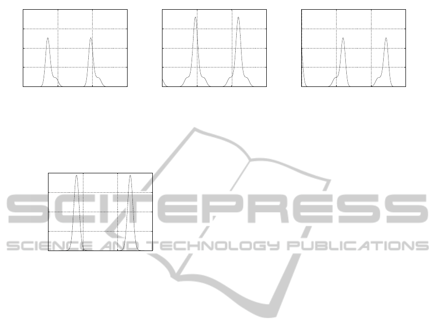
Figure 5: Normalized PSD of the demultiplexed signal at the PIN input for the sensor corresponding to the channel located at
(a) one edge of the spectrum, (b) the middle of the spectrum and (c) on the other edge of the spectrum. Results obtained for
an optical channel spacing of 600 GHz.
0 0.05 0.1 0.15
0
0.2
0.4
0.6
0.8
1
x 10
−3
t [µs]
Voltage [V]
(a)
0.05 0.1 0.15 0.2
0
0.2
0.4
0.6
0.8
1
x 10
−3
t [µs]
Voltage [V]
(b)
0.1 0.15 0.2 0.25
0
0.2
0.4
0.6
0.8
1
x 10
−3
t [µs]
Voltage [V]
(c)
Figure 6: Zoom of the time waveforms of the signal at the PIN output for the sensor corresponding to the channel located at
(a) one edge of the spectrum, (b) the middle of the spectrum and (c) on the other edge of the spectrum. Results obtained for
an optical channel spacing of 600 GHz.
ere is still a small fraction of the adjacent channels
in each demultiplexed signal. This crosstalk power
may be of special relevance from the distortion point
of view. Indeed, as the optical pulses carried by the
different wavelengths may be overlapped in time due
to the walk-off effect, this crosstalk power due to the
adjacent channels that is not completely removed by
the demultiplexing operation can lead to two different
degradation effects: i) if the pulses carried by the de-
sired wavelength and by the ”crosstalk” wavelength
are partially (or totally) overlapped in time, then the
degradation appears as amplitude distortion and ii) if
the pulses carried by the desired wavelength and by
the ”crosstalk” wavelength are not overlapped, then a
fraction of the pulse carried by the ”crosstalk” wave-
length will appear in a time interval where it is not
supposed to be. These conclusions have been drawn
considering un-modulated optical pulses, i. e., with-
out considering the electro-optic conversion of the ra-
dio signals captured by the sensors antennas. How-
ever, it should be stressed that the degradation ef-
fects mentioned above will lead to the same con-
sequence when the entire WDM Ph-ADC system is
working properly: the current at the output of each
photo-detector provides information from the respec-
tive sensor (for instance, if the signal from sensor 1
is modulating the optical wavelength 1, the respective
detected current provides information from sensor 1)
and also information from the sensors that are using
the adjacent wavelengths. This effect is not accept-
able for adequate Ph-ADC operation as the informa-
tion provided by each signal is still used by the digital
signal processing algorithms and may lead to wrong
(or, at least, poor) fingerprinting and localization esti-
mates.
Fig. 6 shows a part of the time waveforms of the
signals at the PIN output for the sensors correspond-
ing to the channels located at the edges and at the mid-
dle of the spectrum (the remaining time waveforms
are similar to the one of Fig. 6(b)). From the analy-
sis of Fig. 6, it is clear that the received signal cor-
responding to each optical wavelength presents dif-
ferent peak amplitudes due to the walk-off effect, as
identified above.
Fig. 7 shows results similar to the ones of
Fig. 6 but considering an optical channel spacing of
400 GHz rather than 600 GHz. Fig. 7 shows that,
when the channel spacing decreases, the crosstalk
of the adjacent channels increases and a fraction of
power appears around the desired optical pulses due
PHOTONIC ANALOGUE-TO-DIGITAL CONVERTER BASED ON WAVELENGTH DIVISION MULTIPLEXING
TECHNIQUE
115
0.025 0.075 0.125 0.175
0
0.5
1
1.5
2
x 10
−3
t [µs]
Voltage [V]
(a)
0.045 0.095 0.145 0.195
0
0.5
1
1.5
2
x 10
−3
t [µs]
Voltage [V]
(b)
0.065 0.115 0.165 0.215
0
0.5
1
1.5
2
x 10
−3
t [µs]
Voltage [V]
(c)
Figure 7: Zoom of the time waveforms of the signal at the PIN output for the sensor corresponding to the channel located at
(a) one edge of the spectrum, (b) the middle of the spectrum and (c) on the other edge of the spectrum. Results obtained for
an optical channel spacing of 400 GHz.
0.06 0.1 0.14 0.18
0
2
4
6
8
x 10
−4
t [µs]
Voltage [V]
Figure 8: Zoom of the time waveform of the signal at the
PIN output for the sensor corresponding to the channel lo-
cated at the middle of the spectrum. Results obtained for an
optical channel spacing of 800 GHz.
to the optical pulses carried by the adjacent wave-
lengths. Notice that, although this fraction of power
only appears in one side of the pulses presented in
Fig. 7(a) and 7(c), it appears in both sides of the pulses
shown in Fig. 7(b) (and also in the pulses correspond-
ing to the remaining two channels that are not pre-
sented in Fig. 7). This is because the signals depicted
in Fig. 7(a) and 7(c) correspond to the channels trans-
mitted at the edges of the WDM spectrum (suffering
from the crosstalk induced by only one adjacent op-
tical channel), while the other signals correspond to
the channels transmitted at the middle of the WDM
spectrum (suffering from the crosstalk induced by two
adjacent optical channels). Fig. 7 shows also that the
amplitude distortion effect is higher than the one ob-
served in Fig. 6 as the crosstalk power is higher due
to the tighter channel spacing used in the results of
Fig. 7.
Fig. 8 depicts part of the time waveform obtained
at the PIN output for the sensor corresponding to the
channel located at the middle of the spectrum, con-
sidering an optical channel spacing of 800 GHz. The
pulses corresponding to the remaining sensors are not
shown as they are identical to the ones of Fig. 8. Fig. 8
shows that there is not any power fraction from adja-
cent optical pulses falling close to the edges of the
desired pulses indicating that the crosstalk due to ad-
jacent channels is negligible. In addition, the com-
parison with the pulses waveform carried by the other
wavelengths showed absence of amplitude distortion
as the pulses carried from the different wavelengths
present similar peak amplitude levels.
Further investigation showed that the absence of
signal degradation due to the walk-off effect is only
reached for optical channel spacing values of the or-
der of 800 GHz. It should be highlighted that, even
with 800 GHz of channel spacing, there is time over-
lapping between the different pulses that comprise
the WDM signal at the 2-nd DEMUX input. How-
ever, the impact of this effect on the different demul-
tiplexedsignals is negligible due to the absence of sig-
nificant crosstalk power imposed by the adjacent op-
tical channels. Considering this 800 GHz of channel
spacing, the entire bandwidth of the multiplexed op-
tical signal used for the WDM Ph-ADC architecture
is around 5×800 GHz=4 THz and, consequently, the
same bandwidth is required for the devices compris-
ing the optical part of the WDM architecture.
4 WDM PH-ADC
ARCHITECTURE OPERATION
IN THE PRESENCE OF
ELECTRICAL SIGNALS
In the previous section, the MUXs/DEMUXs band-
width (400 GHz) and the optical channel spacing
(800 GHz) have been chosen in order to avoid sig-
nificant degradation of the optical pulses and con-
sidering that no electrical signals were modulating
the optical carriers. In this section, the operation
of the WDM Ph-ADC architecture considering the
chosen bandwidth and channel spacing, and taking
OPTICS 2011 - International Conference on Optical Communication Systems
116
−3 −2 −1 0 1 2 3
−100
−90
−80
−70
−60
−50
−40
f [GHz]
PSD [dBm/MHz]
(a)
−3 −2 −1 0 1 2 3
−100
−90
−80
−70
−60
−50
−40
f [GHz]
PSD [dBm/MHz]
(b)
−3 −2 −1 0 1 2 3
−100
−90
−80
−70
−60
−50
−40
f [GHz]
PSD [dBm/MHz]
(c)
−3 −2 −1 0 1 2 3
−100
−90
−80
−70
−60
−50
−40
f [GHz]
PSD [dBm/MHz]
(d)
−3 −2 −1 0 1 2 3
−100
−90
−80
−70
−60
−50
−40
f [GHz]
PSD [dBm/MHz]
(e)
Figure 9: PSD of the time stretched received signal at the output of the BPF of each branch of the electrical receiver.
0 0.05 0.1 0.15 0.2
−0.1
−0.05
0
0.05
0.1
t [µs]
Voltage [V]
(a)
0 0.05 0.1 0.15 0.2
−0.2
−0.1
0
0.1
0.2
t [µs]
Voltage [V]
(b)
0 0.05 0.1 0.15 0.2
−0.2
−0.1
0
0.1
0.2
t [µs]
Voltage [V]
(c)
0 0.05 0.1 0.15 0.2
−0.2
−0.1
0
0.1
0.2
t [µs]
Voltage [V]
(d)
0 0.05 0.1 0.15 0.2
−0.2
−0.1
0
0.1
0.2
t [µs]
Voltage [V]
(e)
Figure 10: Time stretched received signal at the output of the BPF of each branch of the electrical receiver.
into account the signals captured by the five sensors
is analyzed and discussed. The first three orthog-
onal frequency division multiplexing (OFDM) ultra
wideband (UWB) sub-bands centred at 3.43 GHz,
3.96 GHz and 4.49 GHz are considered as the elec-
trical signals captured by the antennas of the different
sensors. The electrical mean power of the OFDM-
UWB signals at the input of the electrical sensor am-
plifiers is -40 dBm and an electrical amplifier gain of
40 dB is used. The gain of the optical amplifier is set
30 dB and the gain of the electrical receiver amplifiers
is adjusted to 50 dB.
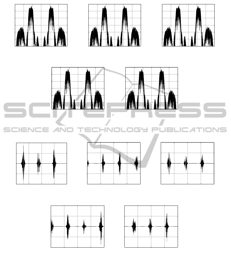
Fig. 9 and 10 depict the PSD and part of the
time waveform of the received time stretched OFDM-
PHOTONIC ANALOGUE-TO-DIGITAL CONVERTER BASED ON WAVELENGTH DIVISION MULTIPLEXING
TECHNIQUE
117

UWB snapshots at the output of the BPF used in each
branch of the electrical receiver of the WDM Ph-ADC
system. Fig. 9 and 10 confirm that time stretching
of the signals at the different branches (and that have
been transmitted in different optical wavelengths) of
the electrical receiver is reached when the WDM ar-
chitecture is employed. Notice that the OFDM-UWB
radio signals centre frequency initially captured by
the sensors antenna appears at the output of the WDM
Ph-ADC compressed by a factor of 3.4 - the time
stretching factor that is being considered. Further in-
vestigation showed that the level of the side lobes of
the spectrum of the compressed signal in the WDM
architecture is similar to the one obtained in the TDM
architecture as it is mainly dependent only on the
EOM (and the same EOM is used for both WDM and
TDM approaches).
5 DISCUSSION ON THE WDM
PH-ADC ARCHITECTURE
PERFORMANCE
In this section, the performance comparison between
the WDM and TDM Ph-ADC architectures is pre-
sented. Particularly, the signal-to-noise ratio (SNR)
evaluated from the approach presented in (Alves and
Cartaxo, 2011) and the degradation due to the fiber
non-linearities are analyzed.
5.1 SNR
In order to compare the SNR of the WDM Ph-ADC
architecture with its TDM version, let’s consider that
the optical peak power of each optical pulsed chan-
nel launched into the fiber in the WDM architecture
is identical to the one of the TDM architecture and
that the lengths of the two spools of fiber are the same
in both architectures. In addition, let’s consider also
that the propagation in both spools of fiber can be
well described as linear transmission. Within these
assumptions and taking into account that the photonic
structure of the WDM architecture is identical to the
one of the TDM architecture, it can be concluded that,
if the same electrical and optical gain levels are con-
sidered for both architectures, and that the insertion
losses imposed by the MUXs/DEMUXs can be ne-
glected, the SNR of the received signal of each branch
of the WDM architecture is identical to the SNR ob-
tained for the time stretched signal at the output of
the TDM architecture. However, the insertion losses
of the MUXs/DEMUXs are usually of the order of a
few dB and may impose some changes on the SNR
levels obtained in the WDM architecture.
In order to assess the SNR levels obtained by
both architectures, the peak SNR (Alves and Cartaxo,
2011) was evaluated for three different gain sets and
considering ideal MUXs/DEMUXs (without insertion
losses) and actual MUXs/DEMUXs (with insertion
losses of 5 dB). The three gain sets represent situa-
tions where the total noise variance is dominantly im-
paired by the noise introduced by the electrical trans-
mitter, by the optical amplifier or by the electrical re-
ceiver. In addition, the optical filter required by the
TDM architecture was modeled by a Gaussian shape
with a -3 dB bandwidth of 400 GHz (identical to the
one of the DEMUXs/MUXs of the WDM architec-
ture) in order to provide a fair comparison between
the results. It should be stressed that, in order to have
a fair comparison, also the same peak power for each
optical pulsed channel launched into the fiber in the
WDM architecture and in the TDM architecture has
been considered. This means that the insertion losses
of the AWG and of the MUX located at the input of
the first spool of fiber are not relevant for the analysis.
Table 1 shows the peak SNR levels obtained for
three cases: the WDM Ph-ADC considering the ab-
sence of MUXs/DEMUXs insertion losses, the WDM
Ph-ADC considering MUXs/DEMUXs with inser-
tion losses of 5 dB and the TDM Ph-ADC archi-
tecture. The results presented in Table 1 confirm
that both architectures provide the same SNR perfor-
mance since the system parameters are identical and
MUXs/DEMUXs with negligible insertion losses are
considered. However, when actual MUXs/DEMUXs
are considered, the peak SNR obtained in the WDM
architecture is lower than the one obtained for the
TDM case. This is due to the influence of the inser-
tion losses of the MUXs/DEMUXs on the power of
the received signal and on the noise variance. In or-
der to clarify this effect, let’s analyze separately the
influence of the insertion losses on each one of the
three different cases of gain sets.
• Total Noise Variance Dominantly Impaired
by the Noise of the Electrical Transmitter
(G
e
=40 dB, G
o
=30 dB, G
r
=50 dB). The total
noise variance is reduced due to the insertion
losses of the MUX and DEMUXs that are lo-
cated at the input and at the output of the second
spool of fiber, respectively. However, the signal
power is further decreased by the insertion losses
of the DEMUX located after the optical amplifier.
Therefore, the SNR obtained for the WDM archi-
tecture is lower than for the TDM.
• Total Noise Variance Dominantly Impaired by
the Noise of the Optical Amplifier (G
e
=20 dB,
G
o
=40 dB, G
r
=50 dB). In this case, the total noise
OPTICS 2011 - International Conference on Optical Communication Systems
118

Table 1: Peak SNR of the TS received signal considering the WDM and TDM Ph-ADC architectures.
G
e
=40 dB G
e
=20 dB G
e
=20 dB
Peak SNR [dB] G
o
=30 dB G
o
=40 dB G
o
=20 dB
G
r
=50 dB G
r
=50 dB G
r
=70 dB
WDM Ph-ADC 27 18 13
without MUXs/DEMUXs ins. losses
WDM Ph-ADC 17 16 -15
with MUXs/DEMUXs ins. losses
TDM Ph-ADC 27 18 13
variance and the signal power are reduced by the
same levelsas the insertion losses of the MUX and
DEMUXs of the optical link affect both in a sim-
ilar way. Hence, the peak SNR obtained for the
WDM architecture should be similar to the one
achieved in the TDM architecture. However, as
the variance due to the ASE noise contribution
is reduced due to the insertion losses, the total
noise variance may not be any more dominantly
impaired by the noise of the optical amplifier. In
this case, the peak SNR of the WDM architecture
is also reduced as it will fall inside one of the two
other cases.
• Total Noise Variance Dominantly Impaired by
the Noise of the Electrical Receiver (G
e
=20 dB,
G
o
=20 dB, G
r
=70 dB). In this situation, the to-
tal noise variance is not affected by the insertion
losses of the MUX and DEMUXs and thus, the
SNR obtained in the WDM architecture is worse
than the one achieved in the TDM as the received
signal power is lower (when compared with the
TDM case) due to the insertion losses.
From the study performed above it is concluded
that it is not possible to obtain higher peak SNRs lev-
els in the WDM architecture than the ones obtained
for the TDM case.
5.2 Fiber Non-linearities
In order to perform a fair comparison, let’s consider
that the optical peak power of each optical pulsed
channel of the WDM architecture is identical to the
one of the optical pulsed signal used in the TDM
architecture and that the pulse repetition rate of the
WDM architecture is maximized (in the Ph-ADC ap-
plication under analysis, it is five times higher than
in the TDM case). In this situation, the total op-
tical average power launched into the first spool of
fiber is higher in the WDM architecture due to the
higher pulse repetition rate. Hence, it is expected
that the signals transmitted over the WDM architec-
ture suffer from higher degradation due to the fiber
non-linearities. As the channel spacing is very large
and the peak power at the optical source output can
exceed 30 dBm, stimulated Raman scattering is very
likely the main multi-channel non-linear impairment.
The detailed quantitative assessment of the degrada-
tion induced by the fiber non-linearities of the WDM
and TDM Ph-ADC architectures on the TS received
signals is out of the scope of this work and will be
presented elsewhere.
6 CONCLUSIONS
The performance operation of the WDM Ph-ADC ar-
chitecture has been analyzed and discussed. The in-
fluence of the -3 dB MUXs/DEMUXs bandwidth and
of the optical channel spacing on the WDM architec-
ture operation has been assessed. The -3 dB band-
width of the MUXs/DEMUXs has been chosen in
order to keep the optical pulses shape at the output
of those devices almost unchanged when compared
with the non-filtered optical pulses. From this study,
a Gaussian shape with -3 dB bandwidth of 400 GHz
has been used to model the MUXs/DEMUXs. The
optical channel spacing between the different optical
channels has been chosen in order to have a negligible
perturbation on the optical pulses due to the crosstalk
induced by the optical pulses carried by the adjacent
optical channels. From this study, an optical channel
spacing of 800 GHz has been chosen for the WDM ar-
chitecture. It has been also shown that when the pro-
posed bandwidth and the optical channel spacing are
used in the WDM architecture using five sensors, ad-
equate time stretching of the OFDM-UWB radio sig-
nals is achieved.
In addition, it has been shown that the WDM ar-
chitecture does not allow obtaining better SNR perfor-
mance than the TDM architecture. It is also expected
that the signals transmitted over the WDM architec-
ture suffer from higher non-linear fiber effects than
the TDM architecture.
From the study performed in this work it is con-
cluded that if the pulse repetition rate is not of special
concern for the localization and fingerprinting algo-
PHOTONIC ANALOGUE-TO-DIGITAL CONVERTER BASED ON WAVELENGTH DIVISION MULTIPLEXING
TECHNIQUE
119

rithms, then the TDM architecture seems to be a bet-
ter solution than the WDM counterpart.
ACKNOWLEDGEMENTS
The work of Tiago Alves was supported by Fundac¸˜ao
para a Ciˆencia e a Tecnologia from Portugal un-
der contract SFRH/BD/29871/2006 and the project
TURBO-PTDC/EEA-TEL/104358/2008. This work
was also supported in part by the EU project
UCELLS-FP7-IST-1-216785. The authors would like
to thank also to UCELLS’ partners by the fruitful dis-
cussions about the structure and the parameters of the
Ph-ADC system.
REFERENCES
Alves, T. and Cartaxo, A. (2011). SNR approach for per-
formance evaluation of time-stretching photonic ana-
logue to digital converter system. Optics Express,
19(2):1493–1509.
Han, Y. and Jalali, B. (2003). Photonic time-stretched
analogue-to-digital converter: fundamental concepts
and pratical considerations. J. Lightwave Technol,
21(12):3085–3103.
Llorente, R., Cartaxo, A., Ugen, B., Duplicy, J., Romme,
J., Puche, J., Schmertz, D., Lostanlen, Y., Banales, R.,
and Marti, J. (2008). Management of UWB picocell
clusters: UCELLS project approach. In Proceedings
of the International Conference on Ultra-Wideband.
IEEE.
Llorente, R., Puche, M. M. J., Romme, J., and Alves, T.
(2009). Sensing ultra-low-power radio signals by pho-
tonic analog-to-digital conversion. In Proceedings
of the European Conference on Optical Communica-
tions.
OPTICS 2011 - International Conference on Optical Communication Systems
120
