
APPLICATION OF SURROGATE MODELING IN
VARIATION-AWARE MACROMODEL AND CIRCUIT DESIGN
Ting Zhu, Mustafa Berke Yelten, Michael B. Steer and Paul D. Franzon
Department of Electrical and Computer Engineering, North Carolina State University, NC 27695, Raleigh, U.S.A.
Keywords: Surrogate modeling, Macromodel, Variation-aware, Circuit, Device model, Design exploration.
Abstract: This paper presents surrogate modeling as a solution to variation-aware macromodeling, circuit design, and
device modeling. A scalable and high-fidelity IO buffer macromodel is created by integrating surrogate
modeling with a physically-based model structure. Circuit performance surrogate models with design and
variation parameters are efficient for design space exploration and performance yield analysis. Surrogate
models of the main device characteristics are generated in order to assess the effects of variability in analog
circuits. Surrogate-based optimization has great potential to speed up complex circuit design.
1 INTRODUCTION
The efforts to create high performance analog/mix-
signal circuits are increasing as system complexities
and uncontrollable variations. It is required to
capture the effects of variations in circuit modeling
and design analysis, in order to create a robustly
behaving design. However, this is a nontrivial task.
In this paper, we apply surrogate modeling to handle
the high-dimensional parameters and complex
responses in variation-aware circuit macromodel,
design analysis, and device model. We demonstrate
the benefits of using surrogate modeling in
enhancing the accuracy, flexibility and efficiency in
those applications.
2 SURROGATE-BASED
MACROMODEL
Large system design and validation are becoming
more and more complex, both in terms of CPU
memory required and simulation time consumed.
Using macromodels of the sub-circuits is a way to
reduce the complexity. We demonstrate a new
methodology of using surrogate modelling in
developing high-fidelity and flexible macromodels.
In the new method, an equivalent circuit structure is
used to capture the static and dynamic circuit
behaviors, while surrogate modeling is used to
approximate each element over a range of Process-
Voltage-Temperature (PVT) parameters, so that the
macromodel is able to dynamically adapt to the PVT
variations in analysis.
2.1 Proposed Macromodel Structure
The new method is applied to develop surrogate-
based Input/Output (IO) buffer macromodel(Zhu and
Franzon, 2009). The most popular approach to IO
modelling is to use the traditional table-based input-
output buffer information specification (IBIS) (IO
Buffer Information Specification, Online). IBIS
models are simple, portable, IP-protected, and fast in
simulation. However, they are unable to simulate
continuous PVT variations and unsuitable for
statistical analysis. We propose a new type of
macromodel, called the surrogate IBIS model, to
solve the problem. Figure 1 shows the proposed
surrogate IBIS macromodel structure that is
composed of physically-based equivalent model
elements. I
pu
and I
pd
represent the nonlinear output
current. Time-variant coefficients K
pu
and K
pd
determine the partial turn-on of the pull-up/down
networks during switching transitions. C
power
and
C
gnd
represent the nonlinear parasitic capacitance
between the output and the supply rails. Global
surrogate modeling techniques (Gorissen et al., 2009)
are used to extract the accurate model elements with
PVT effects. The goal of the global surrogate
modeling is to create a model that approximates the
behavior of the element on the entire domain, so that
the surrogate model expressions can then be used as
a full replacement for the original circuit elements.
502
Zhu T., Berke Yelten M., B. Steer M. and D. Franzon P..
APPLICATION OF SURROGATE MODELING IN VARIATION-AWARE MACROMODEL AND CIRCUIT DESIGN.
DOI: 10.5220/0003649305020508
In Proceedings of 1st International Conference on Simulation and Modeling Methodologies, Technologies and Applications (SDDOM-2011), pages
502-508
ISBN: 978-989-8425-78-2
Copyright
c
2011 SCITEPRESS (Science and Technology Publications, Lda.)

To achieve high-fidelity, data from t ransistor-level
SPICE circuit simulations are used for fitting the
models, and an accuracy target is defined for the
modeling iterations. The surrogate buffer
macromodels obtained are portable and they can be
easily implemented in a variety of modeling
languages, e.g. Verilog-A.
Figure 1: Structural IO buffer macromodel template with
surrogate model elements.
2.2 Macromodel Extraction
The method is demonstrated on a single-ended
output buffer circuit shown in Figure 2. The circuit
is designed in 180 nm CMOS process with a 3.3 V
normal supply voltage. The threshold voltage
variations ΔV
th
in the MOS transistors are
considered as the main process variations and they
are assumed vary by ±20%
.
The supply voltage V
s
is
assumed to fluctuate within ±30% of the nominal
supply (3.3 V) and temperature (T) is set in the range
of 0 to 100
o
C. The Circuit simulations were
performed using HSPICE 2009.03 SP1, and
modeling construction was performed in MATLAB
2009b using the SUMO Toolbox version 7.0.
(Gorissen et al., 2010).
Figure 2: Simplified schematic of the driver circuit.
Figure 3 (a) shows the transistor-level circuit
simulations for modelling pull-up output current
Figure 3: Test-benches for extracting model elements: (a)
pull-up current I
pu
(b) rising/falling transition waveforms
for K
pu
and K
pd
(c) illustration of 2EQ/2UK algorithm (d)
output capacitance C
gnd
and C
power
.
I
pu
(V
S
, V
pu
, T, ΔV
th
). The input signal turns on the
pull-up network and turns off the pull-down network.
Similarly, the pull-down current model I
pd
(V
S
, V
pd
, T,
ΔV
th
) was extracted by turning on the pull-down
network and turning off the pull-up network. The
time-variant transition coefficients K
pu
and K
pd
were
obtained according to 2EQ/2UK algorithm
(Muranyi, Online). Figure 3 (b) shows the test to
obtain the switching output voltage waveforms.
Figure 3(c) shows a simplified circuit to illustrate
the 2EQ/2UK algorithm. The switching output
voltage waveforms wfm
1
and wfm
2
were obtained
with different terminal voltage V
term
, and the
unknown coefficients K
pu
and K
pd
could be derived
by the equations
11
pu pu wfm pd pd wfm out
()(()) ()(()) 0KtIV t KtIV t I
−
−=
22
pu pu wfm pd pd wfm out
() ( ()) () ( ()) 0KtIV t KtIV t I
−
−=
(1)
where
out out term load
()/IVVR
=
−
. I
pu
and I
pd
are the
output current models.
The test setup for extracting the output parasitic
capacitance is shown in Figure 3(d). An AC signal
is attached to the output ports and the imaginary
currents in the power and the ground ports are
measured. The capacitances C
power
and C
gnd
were
derived using
VCC
power
AC
()
2
I
C
f
V
π
ℑ
=
,
gnd
AC
()
2
gnd
I
C
f
V
π
−ℑ
=
(2)
where
VCC
()I
ℑ
and
gnd
()I
ℑ
are the imaginary parts
of the measured currents, f is the frequency of the
AC source, and V
AC
is the AC voltage amplitude.
APPLICATION OF SURROGATE MODELING IN VARIATION-AWARE MACROMODEL AND CIRCUIT DESIGN
503

2.3 Test Results
To implement the new model, we modified the
Verilog-A behavioural version IBIS model (LaBonte
and Muranyi, Online) and applied the surrogate
model expressions for the model elements. The
surrogate models are implemented in the form of
analog functions.
The modified IBIS model and transistor level
model were compared in simulation. The accuracy
of the macromodel is quantified by computing the
timing error and the maximum relative voltage error.
The timing error is defined as the time difference
between the reference and the macromodel voltage
responses measured for crossing half of the output
voltage swing. The maximum relative voltage error
is defined as the maximum error between the
reference and macromodel voltage responses divided
by the voltage swing.
The test setup is shown in Figure 4 where the
driver is connected to a 0.75-m long lossy
transmission line (RLGC model) with a load resistor.
The use of transmission line makes reflections a
very strong concern. The characteristic impedance of
the transmission line is
equal to 50 Ω. The data
pattern for this study is a 1024 bit long
pseudorandom bit sequence (PRBS) with 2-ns bit
time. The lossy transmission line and the loading
resistor R
load
are the same.
Figure 5 shows the responses at the far-end of the
transmission line under the nominal PVT condition
(V
s
= 3.3 V, process parameter ΔV
th
= 0, T = 27 °C).
In this case, the maximum timing error is 70 ps
(3.5% of the bit-time) and the maximum relative
voltage error is 6.45%. We examine the eye diagram
of the output in Figure 5. The eye-width (W) is
measured when the eye-height (H) is equal to 1 V.
The results under different PVT conditions show
that the eye-width differences within 0.04 ns (2% of
the bit-time).
The proposed macromodel achieves good
accuracy in the analysis. The macromodels obtained
show good accuracy in capturing the effects of
reflections and variations, and their scalability
makes flexible design analysis possible.
Figure 4: Test setup for model validation.
Figure 5: Output voltage at far end of transmission line
when input 1024 bit-long PRBS (partial). Grey solid line:
transistor, Black dashed line: macromodel.
2 CIRCUIT DESIGN SPACE
EXLPORATION
Advances in integrated circuit (IC) technologies
have enabled the single-chip integration of multiple
analog and digital functions, resulting in complex
mixed-signal Systems-on-a-Chip (SoCs). Circuit
designers are confronted with large design spaces
and many design variables whose relationships need
to be analyzed. In this situation, tasks such as
sensitivity analysis, design space exploration and
visualization become difficult, even if a single
simulation takes only short time. The analyses are
getting impractical when some of the circuit
simulations are computationally expensive and time-
consuming.
Global surrogate modeling (Gorissen et al., 2009)
could be a valuable asset to assist the circuit design
analysis at an early stage. The method is a data-
driven approximation which is to capture the global
behavior of the circuit by only considering the input
and output behavior. In our experiments, the
surrogate models for the circuit performance (e.g. S-
parameter, gain, power consumption, noise figure,
etc) are constructed with design variables (e.g.
transistor size, bias voltage, current, etc.) as input
parameters. Transistor-level circuit simulations and
performance measurements were setup for obtaining
the modeling data. Adaptive sampling strategies can
be used to make the sampling process interactive
and efficient. An automatic flow is developed for
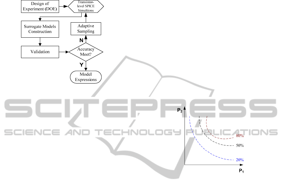
the performance surrogate modeling (Figure 6).
Once the global surrogate model is constructed, it
will help to speed up the sensitivity analysis, to
assist the visualization of the design space, and to
gain insight into the circuit behaviors. The models
SIMULTECH 2011 - 1st International Conference on Simulation and Modeling Methodologies, Technologies and
Applications
504
are reusable so that the designers can vary the
specifications and constraints, and quickly see the
changes in the feasible design space.
Figure 6: Adaptive surrogate-modeling flow with SPICE
circuit simulations.
3 YIELD-AWARE CIRCUIT
DESIGN
As IC technologies scale down to 65 nm and
beyond, it is more challenging to create reliable and
robust designs in the presence of large process (P)
and environmental variations (e.g. supply voltage
(V), temperature(T)) (Semiconductor Industry
Associate). Without considering PVT fluctuations,
the optimal circuit design would possibly minimize
the cost functions by pushing many performance
constraints to their boundaries, and comes up a
design that is very sensitive to the variations.
Therefore, we need to not only search for the
optimal case at the nominal conditions, but also
carefully treat the circuit robustness in the presence
of variations. However, the fulfillment of all these
requirements introduces more complications in
circuit designs.
Yield is defined as the number of dies per wafer
that meet all predefined performance metrics. Monte
Carlo analysis is an important technique used for
yield estimation. However, this method requires a
large number of sampling points to achieve
sufficient accuracy and therefore it is very time-
consuming.
We use performance models with variation
information for quick yield analysis.
(,)PSDV=
JK JK
(3)
Where
D
JK
represents the design parameters, and
V
JK
represents the variation parameters.
The constructed performance models quantize the
dependence among the device-level variations,
design parameters, and the circuit-level performance
so that it can be applied to estimate the performance
yield.
One application of the variation-aware
performance model is to obtain the yield-aware
Pareto fronts which is best trade-offs of the overall
circuit performance and the yield. In addition to
searching for the general Pareto-optimal designs,
performance yield at those design points is evaluated
by using the variation-aware performance model. As
a result, the yield-aware Pareto fronts can be
generated. An illustration is shown in Figure 7. P
1
and P
2
are the performance to trade-off, and the
curves are the Pareto fronts with different yield
levels. The yield-aware Pareto fronts of sub-blocks
could be further used in the yield-aware system
design.
Figure 7: Illustration of Pareto fronts with different yield
levels.
4 SURROGATE-BASED DEVICE
MODELING
Scaling of device sizes induced high variability of
transistor parameters. There are two major reasons
for this. Firstly, quantum mechanics-based
phenomena such as the drain induced barrier
lowering (DIBL) or gate tunnelling which were
negligible in long-channel devices become more
significant. Additional physics-based effects
increased the dependence of many circuit design
quantities including the drain current, I
ds
, and device
transconductance, g
m
, on the transistor process
parameters such as the oxide thickness, t
ox
.
Furthermore, the tolerance of semiconductor
manufacturing components did not scale down as the
transistor sizes shrink (Orshansky et al., 2008). As a
consequence, the amount of uncertainty in the
design quantities remained constant while device
sizes become smaller leading to higher percentages
of variability with respect to the nominal values of
APPLICATION OF SURROGATE MODELING IN VARIATION-AWARE MACROMODEL AND CIRCUIT DESIGN
505

the transistor process parameters. The experimental
data revealed that the traditional process corner
analysis might not reflect the real distribution of the
critical transistor parameters such as the threshold
voltage V
th
(Saha, 2010) while the Monte Carlo
analysis become more computationally intensive
with increasing number of variability factors.
The response surface of design quantities which
become more complex with the presence of extreme
process variations can be accurately captured by
surrogate modelling. Surrogate modelling aims to
express the output quantity in terms of a few input
parameters by evaluating a limited number of
samples. These samples are employed by the basis
functions which establish the response surface of the
desired output. Coefficients of the basis functions
should be optimized to minimize the modelling
error. This approach has been applied to the problem
of I
ds
modelling in order to assess the effects of
variability in analogue circuit building blocks, in
particular, the differential amplifiers (Yelten et al.,to
be published). In this paper, the modelling of g
m
of
n-channel transistors will be discussed.
g
m
is an important quantity for analogue circuits,
particularly in determining the AC performance of
amplifiers, mixers and voltage controlled oscillators.
The modelling here is based on 65 nm device
technology (IBM 10SF design kit) and uses six
process parameters (t
ox
, intrinsic threshold voltage
V
th,0
, intrinsic drain-source resistance R
ds,0
, intrinsic
mobility µ
0
, channel length variation ΔL
eff
, and
channel doping N
ch
) as input to the model in addition
to the terminal voltages of the transistor (gate-source
voltage V
gs
, drain-source voltage V
ds
, and bulk-
source voltage V
bs
) and the temperature T. The
choice of these process parameters is based on their
physical origin which ensures a weak correlation
between each parameter. BSIM model I
ds
equations
are analytically differentiated to yield g
m
such that:
.
mdsgs
g
IV=∂ ∂
(4)
The g
m
expression is validated by extensive
SPICE circuit simulations over the process corners
and at temperature extremes so that it can be used to
evaluate the samples, each composed of the ten
elements described above. Although an analytic
equation for g
m
is used in this work, the modelling
methodology is general and can employ simulations
or measurement results given that they have the
same input and output parameters.
Kriging basis functions are used to construct the
surrogate model with the necessary coefficients
being optimized using the MATLAB toolbox Design
and Analysis of Computer Experiments (DACE)
(Lophaven et al., URL). The device width is
assumed to be 10 µm. The finalized model is tested
for accuracy using the root relative square error
(RRSE) metric where RRSE can be given as:
() ()
()
() ()
2
mod
1
2
11
RRSE .
1
T
TT
N
el true
i
NN
true true
ii
T
yiyi
yi yi
N
=
==
−
=
⎛⎞
−
⎜⎟
⎝⎠
∑
∑∑
(5)
In (5), N
T
is the number of test samples. The g
m
model is constructed using a total number of 2560
input samples, and tested with N
T
=6400 samples
other than the input samples. The resulting model
yields an RRSE of 3.96% indicating to a high level
of accuracy.
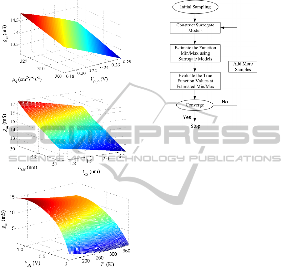
The model can be used to observe the changes in
g
m
with respect to its input parameters. Examples of
this are provided in Figure 8. The graphs provide
critical insight to the designer about the fundamental
relations and trade-offs between the chosen process
parameters, terminal voltages and temperature.
5 SURROGATE-BASED CIRCUIT
OPTIMIZATION
Simulation-based circuit optimization creates a good
opportunity for surrogate modeling, as the process
requires a great number of iterative evaluations of
objective functions. In optimization process,
surrogate models are used to guide the search
instead of achieving the global accuracy.
In the surrogate-based optimization process,
generally there are two types of simulation models, a
low-fidelity and a high-fidelity model. In our circuit
design problems, the transistor-level circuit
simulation is used for high-fidelity model while the
built surrogate model is used for low-fidelity model.
The general surrogate-based optimization process is
shown in Figure 9 (Queipo et al., 2005).
We are interested in exploring Gaussian process
based model (e.g. Kriging model) as an
approximation method since Kriging model is able
to provide estimation of the uncertainty in the
prediction. Adaptive sampling methods (e.g.
expected improvement (Forrester et al.,2008)) can
be used to balance between the exploration
(improving the general accuracy of the surrogate
model) and exploitation (improving the accuracy of
the surrogate model in the local optimum area)
during optimization. An alternative method, space
mapping (Koziel et al., 2008),
maps the input/output
SIMULTECH 2011 - 1st International Conference on Simulation and Modeling Methodologies, Technologies and
Applications
506
(a)
(b)
(c)
Figure 8: 3D graphs showing the trade-offs between the
different inputs on the modelled gm.
space of a low-fidelity model to the input/output
space of the high-fidelity model. These methods
would be able to significantly improve the
optimization efficiency when physically
computational cheap low-fidelity models are
available.
6 SUMMARY
This work presents the applications of surrogate
modelling in variation-aware circuit modeling and
Figure 9: General surrogate-based optimization flow.
design analysis. Surrogate modeling enhances the
accuracy and flexibility of IO macromodel, assets
the design exploration and optimization with, and
generates device model with critical variability
parameters. The surrogate-based method
demonstrates great benefits of reducing the complex
and cost in variation-aware modeling and circuit
design.
ACKNOWLEDGEMENTS
This material is based upon work supported by the
Defense Advanced Research Projects Agency and
the Air Force Research laboratory in the project
“Algorithms and Structures For Self Healing
Circuits” under contract number FA8650-09-7925 as
a subcontract to Raytheon as part of DARPA’s Self
Healing Mixed Signal Integrated Circuits
(HEALICS) program. The authors T. Zhu, Dr. P. D.
Franzon, and Dr. M. B. Steer would like to thank Dr.
T. Dhaene of Ghent University, Belgium, for
providing SUrrogate MOdeling (SUMO) Toolbox
and for helpful discussion.
REFERENCES
T. Zhu and P.D. Franzon.“ Application of
surrogatemodeling to generate compact and PVT-
sensitive IBIS models,” in Proc. 18th Electrical
Performance of Electronic Packaging and Systems,
Portland, OR., pp. 77-80, Oct. 19-21, 2009.
IO Buffer Information Specification [Online]. Available:
APPLICATION OF SURROGATE MODELING IN VARIATION-AWARE MACROMODEL AND CIRCUIT DESIGN
507

http://www.eigroup.org/ibis/ibis.htm.
D. Gorissen, F. De Turck and T. Dhaene, “Evolutionary
model type selection for global surrogate modeling,”
Journal of Machine Learning Research, vol. 10, No. 1,
pp. 2039-2078, Sep. 2009.
D. Gorissen, K. Crombecq, I. Couckuyt, T. Dhaene and P.
Demeester, “A surrogate modeling and adaptive
sampling toolbox for computer based design,” Journal
of Machine Learning Research, vol. 11, pp. 2051-2055,
Jul. 2010.
A. Muranyi, “Accuracy of IBIS models with reactive
loads,” [online] Available: http://www.eda.org/pub/
ibis/summits/feb06/muranyi2.pdf
M. LaBonte and A. Muranyi, “IBIS Advanced Technology
Modeling Task Group Work-achievement: Verilog-A
element library HSPICE test,” [online]. Available:
http://www.vhdl.org/pub/ibis/macromodel_wip/
archive-date.html.
Semiconductor Industry Associate, International
Technology Roadmap for Semiconductors ITRS.
M. Orshansky, S. R. Nassif, and D. Boning, Design for
Manufacturability and Statistical Design: A
constructive Approach, Springer: New York, USA,
2008.
S. K. Saha, “Modeling process variability in scaled CMOS
technology,” IEEE Des. Test. Comput., vol. 27, no. 2,
pp. 8-16, 2010.
M. B. Yelten, P. D. Franzon, M. B. Steer, “Surrogate
model-based analysis of analog circuits—Part I:
Variability Analysis,” IEEE Trans. Device Mater.
Rel., to be published.
S. N. Lophaven, H. B. Nielsen and J. Søndergaard, A
MATLAB Kriging toolbox 2.0 Aug2002, URL:
http://www2.imm.dtu.dk/˜hbn/dace/dace.pdf.
N. V. Queipo, R. T. Haftka, W. Shyy, T. Goel, R.
Vaidyanathan and P. K. Tucker, “Surrogate-based
analysis and optimization,” Progress in Aerospace
Sciences, vol. 41, pp. 1–28, Feb. 2005.
A. Forrester, A. Sobester, and A. Keane, Engineering
Design via Surrogate Moldeling: A Practical Guide,
John Wiley & Sons, Sep. 2008.
S. Koziel, Q.S. Cheng, and J.W. Bandler, “Space
mapping,” IEEE Microwave Magazine, vol. 9, no. 6,
2008, pp. 105-122
SIMULTECH 2011 - 1st International Conference on Simulation and Modeling Methodologies, Technologies and
Applications
508
