
ADDRESSING THE HARDWARE RESOURCE REQUIREMENTS
OF NETWORK-ON-CHIP BASED NEURAL ARCHITECTURES
Sandeep Pande, Fearghal Morgan, Seamus Cawley, Brian Mc Ginley
Bio-Inspired Electronics and Reconfigurable Computing, National University of Ireland, Galway, Ireland
Jim Harkin, Snaider Carrillo, Liam Mc Daid
Intelligent Systems Research Centre, University of Ulster, Magee Campus, Derry, Northern Ireland
Keywords: Spiking Neural Networks (SNN), Synaptic connectivity, Neural network topology memory, Network on
Chip (NoC).
Abstract: Network on Chip (NoC) based Spiking Neural Network (SNN) hardware architectures have been proposed
as embedded computing systems for data/pattern classification and control applications. As the NoC
communication infrastructure is fully reconfigurable, scaling of these systems requires large amounts of
distributed on-chip memory for storage of the SNN synaptic connectivity (topology) information. This large
memory requirement poses a serious bottleneck for compact embedded hardware SNN implementations.
The goal of this work is to reduce the topology memory requirement of embedded hardware SNNs by
exploring the combination of fixed and configurable interconnect through the use of fixed sized clusters of
neurons and NoC communication infrastructure. This paper proposes a novel two-layered SNN structure as
a neural computing element within each neural tile. This architectural arrangement reduces the SNN
topology memory requirement by 50%, compared to a non-clustered (single neuron per neural tile) SNN
implementation. The paper also proposes sharing of the SNN topology memory between neural cluster
outputs within each neural tile, for utilising the on-chip memory efficiently. The paper presents hardware
resource requirements of the proposed architecture by mapping SNN topologies with random and irregular
connectivity patterns (typical of practical SNNs). The architectural scheme of sharing the SNN topology
memory between neural cluster outputs, results in efficient utilisation of the SNN topology memory and
helps accommodate larger SNN applications on the proposed architecture. Results illustrate up to a 66%
reduction in the required silicon area of the proposed clustered neural tile SNN architecture using shared
topology memory compared to the non-clustered, non-shared memory architecture.
1 INTRODUCTION
Biologically-inspired computing paradigms such as
evolutionary computing and neural networks provide
promising solutions for designing complex and
intelligent embedded systems (Marrow, 2000). The
organic central nervous system includes a dense and
complex interconnection of neurons and synapses,
where each neuron connects to thousands of other
neurons through synaptic connections. Computing
systems based on Spiking Neural Networks (SNNs)
emulate real biological neural networks, conveying
information through the communication of short
transient pulses (spikes) between neurons via their
synaptic connections. Each neuron maintains a
membrane potential, which is a function of incoming
spikes, synaptic weights, membrane potential, and
membrane potential leakage coefficient (Maass,
1997); (Gerstner and Kistler, 2002). A neuron fires
(emits a spike to all connected synapses/neurons)
when its membrane potential exceeds the neuron’s
firing threshold value. Brain-inspired computing
paradigms such as SNNs offer the potential for
elegant, low-power and scalable methods of
embedded computing, with rich non-linear
dynamics, ideally suited to applications including
data/pattern classification, dynamic control and
signal processing. The efficient implementation of
SNN-based hardware architectures for real-time
embedded systems is primarily influenced by neuron
design, scalable on-chip interconnect architecture,
128
Pande S., Morgan F., Cowley S., Mc Ginley B., Harkin J., Carrillo S. and Mc Daid L..
ADDRESSING THE HARDWARE RESOURCE REQUIREMENTS OF NETWORK-ON-CHIP BASED NEURAL ARCHITECTURES.
DOI: 10.5220/0003676601280137
In Proceedings of the International Conference on Neural Computation Theory and Applications (NCTA-2011), pages 128-137
ISBN: 978-989-8425-84-3
Copyright
c
2011 SCITEPRESS (Science and Technology Publications, Lda.)

and SNN training/learning algorithms (Maguire et
al., 2007).
The authors have proposed and investigated
EMBRACE as an embedded computing element for
implementation of large scale SNNs (Jim Harkin et
al., 2009). The proposed EMBRACE mixed-signal
architecture incorporates compact, low power, high-
resolution CMOS-compatible analogue neuron cells,
interconnected using a packet switched Network on
Chip (NoC) architecture.
Directly connecting neuron circuits within large
scale hardware SNN is not viable in VLSI
architectures because of high fan-out and
interconnection requirements. The NoC approach
exploited within EMBRACE provides flexible,
packet-switched inter-neuron communication
channels, scalable interconnect and connection
reconfigurability (Benini and De Micheli, 2002);
(Vainbrand and Ginosar, 2010); (F. Morgan et al.,
2009).
For hardware SNN implementations, the SNN
topology information includes neural circuit
connectivity data for each synapse in the system.
Scaling of NoC-based hardware SNN systems
requires large amounts of distributed on-chip
memory for storage of the SNN synaptic
connectivity (SNN topology) information. This large
memory requirement poses a serious bottleneck for
compact embedded hardware SNN implementation.
This paper proposes clustering of neurons within
neural tiles in order to reduce the overall SNN
topology memory requirement by 50% compared to
the previously reported single neuron per NoC router
SNN architecture (Jim Harkin et al., 2009). Each
clustered neural tile comprises a fully connected
feed-forward SNN structure. Fixed connections
between the neurons in the neural cluster remove the
requirement for storage of connection topology
memory. The paper describes the architecture of the
neural cluster element (made-up of a two layer fully
connected feed-forward SNN structure) and the
neural tile. The use of fixed sized SNN structure as a
neural element can result in constrain mapping of
certain SNN application topology, which can be
addressed by using additional neural clusters as
spike repeaters.
The paper also proposes a further architectural
enhancement, which involves sharing the SNN
topology memory (within each neural tile) between
neural cluster outputs. The paper describes the
shared SNN topology memory partitioning and
operation. SNN topology memory blocks are
allocated to each active cluster output based on its
synaptic connectivity requirements. The scheme
offers flexible synaptic connectivity for SNN
application topologies. The proposed clustered
neural tile, and shared topology memory hardware
SNN architecture is analysed with a range of SNN
application topologies exhibiting irregular
connectivity typically seen in real-life SNN
application topologies (Kohl and Miikkulainen,
2008). Hardware resource requirements for each
element of the proposed clustered neural tile SNN
architecture using shared topology memory are
compared to the single neuron per NoC router
EMBRACE hardware SNN architecture reported in
(Fearghal Morgan et al., 2009) (using recently
reported 32nm CMOS VLSI technology). Results
illustrate up to a 66% reduction in the required
silicon area of the proposed clustered neural tile
SNN architecture using shared topology memory
compared to the reported single neuron per router
EMBRACE hardware SNN.
The structure of the paper is as follows: Section
2 summarises the current research in hardware SNN
architectures, and SNN topology memory resource
requirements. The previously reported EMBRACE
NoC-based hardware SNN reference architecture
and its hardware resource requirements is described
in section 3. The proposed neuron clustering and
shared SNN topology memory architecture are
presented in Section 4. Section 5 presents
significance of the shared SNN topology memory
scheme by mapping SNN applications representing
practical connectivity patterns to the proposed
architecture. Section 6 concludes the paper and
proposes future work.
2 STATE-OF-THE-ART
HARDWARE SNN
ARCHITECTURES
Inspired by biology, researchers aim to implement
reconfigurable and highly interconnected arrays of
neural network elements in hardware to produce
powerful signal processing units (Jim Harkin et al.,
2009); (Yajie Chen et al., 2006); (Furber and Brown,
2009); (Upegui et al., 2005); (Pearson et al., 2007);
(Ros et al., 2006); (R. J. Vogelstein et al., 2007);
(Ehrlich et al., 2007); (B. Glackin et al., 2005);
(Schemmel et al., 2008). For large scale hardware
implementation of SNNs, the neuron interconnect
imposes problems due to high levels of inter-neuron
connectivity and often the number of neurons that
can be realised in hardware is limited by high fan
in/out requirements (L. P. Maguire et al., 2007).
ADDRESSING THE HARDWARE RESOURCE REQUIREMENTS OF NETWORK-ON-CHIP BASED NEURAL
ARCHITECTURES
129

Direct neuron-to-neuron interconnection exhibits
switching requirements that grow non-linearly with
the network size. Efficient, low area and low power
implementations of neuron interconnect and synaptic
junctions are key to scalable hardware SNN
implementations (L. P. Maguire et al., 2007).
(Ros et al., 2006) present an FPGA-based hybrid
computing platform. The neuron model is
implemented in hardware and the network model
and learning are implemented in software. (B.
Glackin et al., 2005) uses a time multiplexing
technique to implement large SNN models (with
>1.9M synapses and 4.2K neurons), implemented in
software, where speed-acceleration is the key
motivation, and the parallel capability of SNNs is
not exploited. Clustered connections based neural
network architecture using NoC and method for
mapping of SNNs to the architecture has been
proposed in (Emery et al., 2009).
Analogue spiking neuron design approaches can
benefit from a compact area implementation due to
their inherent similarity with the way electrical
charge flows in the brain (Yajie Chen et al., 2006);
(Yajie Chen et al., 2008); (R. J. Vogelstein et al.,
2007). These architectures rely on digital
components for a flexible communication
infrastructure. (Ehrlich et al., 2007) and (Schemmel
et al., 2008) present FACETS, a configurable wafer-
scale mixed-signal neural ASIC system. The work
proposes a hierarchical neural network and the use
of analogue floating gate memory for synaptic
weights. (R. J. Vogelstein et al., 2007) presents a
mixed-signal SNN architecture of 2,400 analogue
neurons, implemented using switched capacitor
technology and communicating via an asynchronous
event-driven bus. The chip area is reported to be
3mm x 3mm using 0.5µm CMOS VLSI technology.
Practical SNN systems are characterised by large
numbers of neurons and high interconnectivity
through inter-neuron synaptic connections. Each of
the SNN execution architectures presented in
(Ehrlich et al., 2007); (Schemmel et al., 2008);
(Furber and Brown, 2009); (Ros et al., 2006);
(Upegui et al., 2005); (Pearson et al., 2007); (B.
Glackin et al., 2005); (Vogelstein et al., 2007) aim
for thousands of neurons and millions of synapses.
Due to the high neuron interconnectivity, synaptic
connectivity information is stored in off-chip
DRAMs and is accessed using memory controllers.
The neural computing kernel must be supplied with
this connectivity information for calculation of spike
generation and transfer events in the system; this
synaptic connectivity information storage strategy
results in high memory traffic and increased power
consumption, unsuitable for embedded system
implementation.
The NoC design paradigm provides a promising
solution for the flexible interconnection of large
SNNs (Vainbrand and Ginosar, 2010). The
SpiNNaker project (Furber and Brown, 2009) aims
to develop a massively parallel computer capable of
simulating SNNs of various sizes, topology and with
programmable neuron models. The SpiNNaker
architecture uses ARM-968 processor-based nodes
for computation and an off-chip NoC
communication infrastructure. Each NoC tile in the
SpiNNaker system models 1000 Leaky-Integrate-
Fire neurons, each having 1000 synapse inputs. Each
SpiNNaker node requires approximately 4MBytes
of memory for storing synaptic connectivity
information (Furber et al., 2006). Hence, the
SpiNNaker architecture stores the synaptic
connection data in off-chip SDRAM. Due to low-
power and area requirements of embedded systems
targeted by EMBRACE NoC-based SNN
architecture, use of off-chip SDRAM and associated
memory controllers is not feasible.
3 EMBRACE: HARDWARE SNN
ARCHITECTURE
This section describes the previously reported
EMBRACE NoC-based hardware SNN architecture
and its hardware resource requirements. EMBRACE
(Jim Harkin et al., 2009) uses a single neuron per
neural tile (non-clustered) SNN implementation and
provides a reference for the work of this paper.
The EMBRACE mixed-signal architecture
(currently prototyped digitally, Figure 1) ultimately
aims to incorporate low-power CMOS-compatible
analogue neural cell circuits, and a digital NoC-
based packet switching interconnect, to realise a
scalable SNN execution architecture suitable for
embedded systems. This architectural scheme has
potential to offer high synaptic densities while
maintaining compact silicon implementation area
and low power consumption.
The EMBRACE NoC-based SNN architecture
(Figure 1) is a two-dimensional mesh topology array
of neural elements (N) and NoC Routers (R). The
architecture comprises a single neuron per NoC
router, where each neuron within the NoC tile
supports 64 input synapses and its output can
connect to maximum 64 synaptic connections. (This
architecture is referred as non-clustered EMBRACE
architecture in the rest of the paper).
NCTA 2011 - International Conference on Neural Computation Theory and Applications
130
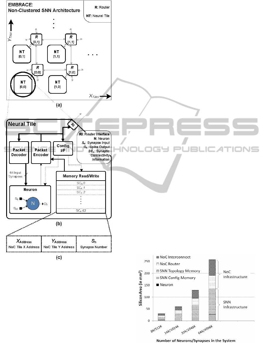
Figure 1: (a) EMBRACE NoC-based SNN Architecture,
(b) Neural Tile Comprising Single Neuron, Packet
Encoder/Decoder and SNN Topology Memory and (c)
Synaptic Connection Information.
The SNN topology memory within EMBRACE
architecture defines each inter-neuron synaptic
connection. The EMBRACE architecture template
(Figure 1) requires 11MB of SNN topology memory
to support 64K neuron/4M synapse hardware SNN.
NoC router is connected in North (N), East (E),
South (S) and West (W) directions, forming a
Manhattan-style, two-dimensional mesh topology
NoC architecture. An application specific SNN is
realised on the EMBRACE architecture by
programming neuron configuration parameters
(SNN synaptic weights and neuron firing threshold
potential) and SNN connection topology. Spike
communication within the SNN is achieved by
routing spike information within spike data packets
over the network of routers. The authors have
implemented and reported EMBRACE-FPGA
(Morgan et al., 2009c), an FPGA prototype
implementation of the EMBRACE architecture. The
EMBRACE-FPGA prototype has been successfully
applied to benchmark SNN control and classifier
applications (such as pole balancer, two-input XOR
and Wisconsin cancer dataset classifier).
EMBRACE-SysC, a SystemC-based, clock cycle
accurate simulation and performance measurement
platform for simulation and analysis of EMBRACE
architecture has been reported (Sandeep Pande et al.,
2010). EMBRACE-SysC enables rapid NoC
architectural exploration and analysis of the
EMBRACE architecture.
3.1 Hardware Resource Requirements
Compact hardware implementation of SNN
architectures is essential for their use in portable
embedded systems. This section estimates the
hardware resource requirements of the non-clustered
EMBRACE architecture. The transistor count and
chip area is estimated for the non-clustered
EMBRACE architecture in recent CMOS VLSI
implementation technology to understand the
practicality of realising EMBRACE SoC in silicon.
The silicon area required for implementation of
the non-clustered EMBRACE architectural template
(depicted in Figure 1) is estimated using recently
reported 32nm CMOS VLSI technology. Figure 2
presents the estimated silicon die area (in mm
2
) by
scaling the non-clustered EMBRACE architecture.
Figure 2: Silicon Area Estimate (using 32nm CMOS
technology) for the EMBRACE non-clustered
architecture.
ADDRESSING THE HARDWARE RESOURCE REQUIREMENTS OF NETWORK-ON-CHIP BASED NEURAL
ARCHITECTURES
131
The x-axis indicates the number of neurons and
synapses (Neuron/Synapse). The stacked columns in
the histogram denote the silicon area for each
architectural entity described below:
NoC Infrastructure: The NoC infrastructure
comprises NoC routers, packet buffers, NoC
interconnect and associated control circuits. The
total number of bits in all the storage elements
within digital components is summed and the
required number of transistor estimated based on the
standard SRAM cell design. The transistor count for
control circuitry within the digital components is
proportional to the transistor count of the storage
circuits. The NoC interconnect (point-to-point bus
links between NoC routers) area is estimated based
on the bus width and the metal layer routing offered
by the VLSI implementation technology. The
analytical estimates indicate that complete NoC
infrastructure requires 47.27% of the total chip area.
SNN Infrastructure: The silicon area for the
EMBRACE analogue neural elements (including
synapses, synaptic weight summing and membrane
potential threshold device), is calculated using the
design and characterisation data reported in (Yajie
Chen et al., 2006a); (Yajie Chen et al., 2008); (Yajie
Chen et al., 2006b). Due to its compact
implementation, the silicon area occupied by neural
elements is negligible in comparison to rest of the
SNN support infrastructure. The SNN support
infrastructure is made-up of SNN configuration
memory (for storing synaptic weights of 5 bits each
and threshold values of 16 bits each) and the SNN
topology memory (for storing synaptic connectivity
information) (Seamus Cawley et al., 2011). Silicon
area of the SNN infrastructure is estimated using the
above mentioned estimation technique and requires
52.74% of the total chip area. Figure 3 further
enumerates the silicon area of the SNN components
for the 64K Neuron non-clustered EMBRACE
architecture.
Figure 3: Estimated Silicon Area Proportion for the SNN
Infrastructure Entities for 64K Neurons/4M Synapses
Non-Clustered EMBRACE Architecture Configuration.
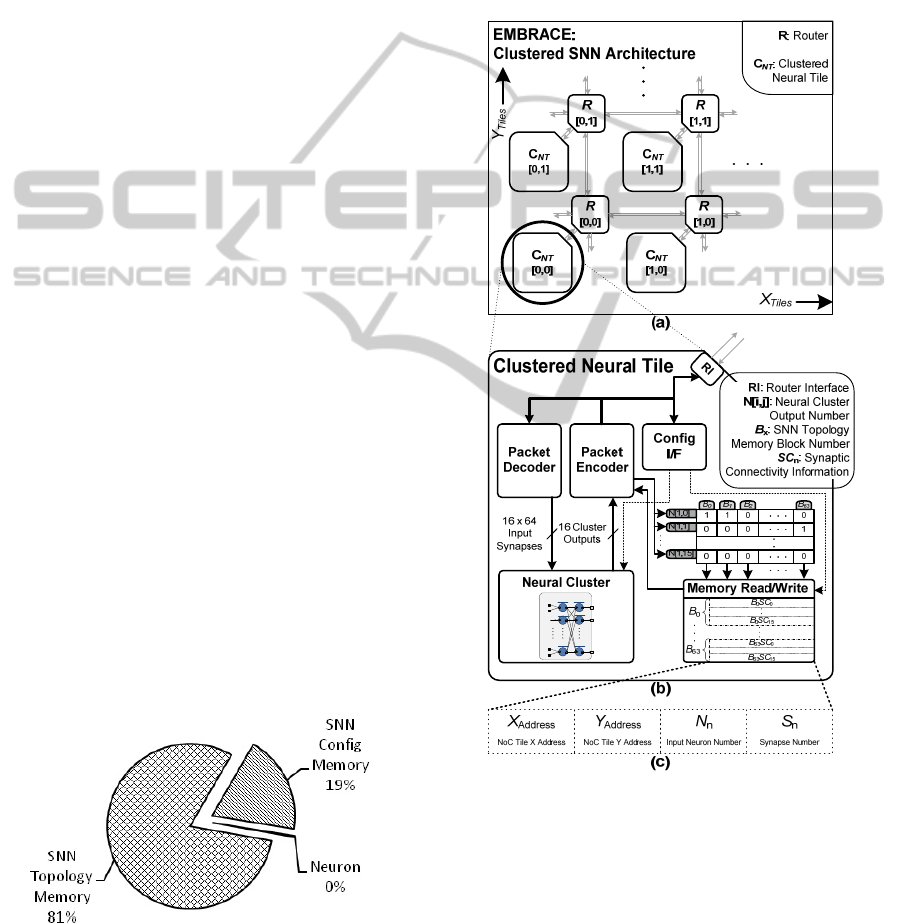
Figure 3 illustrates that the SNN topology
memory accounts for 81% and the SNN
configuration memory accounts for 19% of the area
required by the SNN components.
4 NOVEL CLUSTERED NEURAL
TILE HARDWARE SNN
ARCHITECTURE
Figure 4: The Proposed EMBRACE Clustered SNN
Architecture, (b) Clustered Neural Tile Comprising Neural
Cluster, Packet Encoder/Decoder, Shared SNN Topology
Memory and Look-up Table, and (c) Synaptic Connection
Entry.
Architectural techniques for reducing the SNN
topology and configuration memory are vital for
compact silicon implementation of hardware SNN
architectures suitable for embedded computing. This
section presents clustering of neurons in the NoC tile
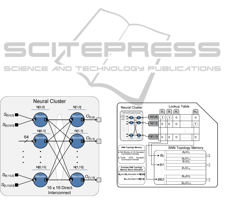
16 x 16 SNN Structure
Neuron
N[0,0]
Neuron
N[0,1]
Neuron
N[0,15]
Neuron
N[1,0]
Neuron
N[1,1]
Neuron
N[1,15]
S
{0,0,0}
S
{0,0,63}
S
{0,15,0}
S
{0,15,63}
O
{1,0}
O
{1,1}
O
{1,15}
64
NCTA 2011 - International Conference on Neural Computation Theory and Applications
132
and architectural scheme for sharing of the SNN
topology memory within the NoC tile for compact
implementation of the proposed EMBRACE
architecture. Silicon area requirements for the
proposed clustered neural tile NoC architecture are
compared with those of the non-clustered
EMBRACE architecture.
Figure 4 illustrates the proposed clustered SNN
architecture, clustered neural tile architecture
andsynaptic connection entry details.
4.1 Neural Cluster
Permanent interconnection between neurons within
the neural cluster removes the need to store synaptic
connectivity information within the cluster. For
hardware implementations, size of the SNN structure
formed using the direct connections can be extended
based on the permitted fan-out of individual neuron
circuits. Also, the metal layer routing in the VLSI
architectures cannot efficiently accommodate large
sized interconnect crossbars without increasing the
inter-metal capacitance and crosstalk. A two-layered
16:16 fully connected feed-forward SNN structure
(shown in Figure 5) is proposed as the neural
computing element inside each NoC tile.
Figure 5: Two layered 16:16 Fully Connected SNN
Structure as the Proposed Neural Cluster.
The input and output layer of the neural cluster
comprises 16 Leaky-Integrate-and-Fire neurons. The
input layer neurons have 64 input synapses each,
which receive spikes from synaptic connections
external to the NoC tile. Each of the 16 input layer
neurons connects directly to each of the 16 output
layer neurons, to form a fully connected feed-
forward SNN structure. Each output layer neuron
has 16 input synapses, which individually receive
spikes from the corresponding input layer neurons.
The neural cluster has 16 outputs each
corresponding to the 16 output layer neurons.
4.2 Shared SNN Topology Memory
Architecture
Figure 6 illustrates the internal organisation of the
clustered neural tile comprising the fixed-sized
neural cluster, SNN topology memory and the
associated look-up table.
The synaptic connection information for the
neural cluster outputs is stored in the SNN topology
memory. The synaptic connection information entry
comprises destination tile address ([X,Y] address of
the NoC tile), destination neuron (N
n
) and synapse
number (S
n
) (see Figure 4). The SNN topology
memory is partitioned into 64 blocks (B
0
to B
63
),
where each block is made-up of 16 synaptic
connection information entries (B
x
SC
0
to B
x
SC
15
).
This block-wise partitioning arrangement helps
flexible allocation of the SNN topology memory
blocks to different neural cluster outputs on need
basis.
Figure 6: The Clustered Neural Tile Internal Organisation,
Comprising Neural Cluster, SNN Topology Memory and
the Associated Look-up Table.
The synaptic connection information for the
neural cluster outputs is stored in the SNN topology
memory. The synaptic connection information entry
comprises destination tile address ([X,Y] address of
the NoC tile), destination neuron (N
n
) and synapse
number (S
n
) (see Figure 4). The SNN topology
memory is partitioned into 64 blocks (B
0
to B
63
),
16 Output Synaptic
Connections per Block
ADDRESSING THE HARDWARE RESOURCE REQUIREMENTS OF NETWORK-ON-CHIP BASED NEURAL
ARCHITECTURES
133

where each block is made-up of 16 synaptic
connection information entries (B
x
SC
0
to B
x
SC
15
).
This block-wise partitioning arrangement helps
flexible allocation of the SNN topology memory
blocks to different neural cluster outputs on need
basis.
The lookup table maintains the SNN topology
memory block allocation information for each neural
cluster output. Each neural cluster output has a
designated row in the lookup-table. Each bit in the
64-bit lookup table row allocates the corresponding
memory block from the SNN topology memory to
the neural cluster output. For example, bit number
B
x
of the row number N[1,0] allocates block number
X in the SNN topology memory to the neural cluster
output N[1,0]. (i.e. For the row number N[1,0],
setting the bit value B
x
= 1, allocates the SNN
topology memory block X to cluster output N[1,0];
whereas Bit value B
x
= 0 dissociates the SNN
topology memory block X from cluster output
N[1,0]). The packet encoder generates spike packets
for the cluster output based on the allocated SNN
topology memory blocks for the cluster output. The
process of mapping the SNN application topology
onto the proposed clustered neural tile, shared
memory architecture involves populating the lookup
table and SNN topology memory entries, such that
the correct synaptic connections are established
between the neural clusters. If the synaptic
connectivity for a neural cluster cannot be
accommodated in the given SNN topology memory
available in the NoC tile, additional neural cluster
and NoC tiles are use as spike repeaters.
4.3 Architectural and SNN Application
Significance
This section compares the proposed clustered neural
tile architecture with the non-clustered EMBRACE
architecture for silicon area requirements and
number of synapses supported.
4.3.1 Silicon Area Requirements
The silicon area for implementation of the proposed
clustered neural tile NoC architectural template
(shown in Figure 4) is estimated using 32nm CMOS
VLSI technology. Figure 7 illustrates the
comparison of silicon area by scaling the non-
clustered EMBRACE and the proposed clustered
neural tile NoC architecture.
Figure 7: Silicon Area Estimate Comparison for the Non-
Clustered EMBRACE Architecture and the proposed
Clustered Neural Tile SNN Architecture.
Each NoC tile in the clustered architecture
comprises 32 neurons served by a NoC router as
compared to the non-clustered architecture (which
has a single neuron for each NoC router). Thus, the
total number of NoC routers in the system are
decreased by a factor of 32 (i.e. the number of
neurons in the neural cluster) as compared to the
non-clustered architecture. In the proposed clustered
neural tile NoC architecture, the packet buffers
inside each NoC router are increased by a factor of
16 to accommodate higher spike packet traffic
density in the NoC. Due to the reduced number of
NoC routers, the area occupied by the NoC
infrastructure in the proposed clustered neural tile
NoC architecture is decreased by 89% as compared
to the previously reported non-clustered architecture.
The fixed interconnection within the neural
cluster removes the need for storing the output
synaptic connectivity information for the input layer
neurons within the neural cluster. The regularly
structured interconnect requires much less area than
the SRAM-based synaptic connectivity storage and
the associated control circuitry. Hence, the SNN
topology memory for the proposed clustered neural
tile NoC architecture is reduced by 54.05%. The size
of the complete chip is approximately 33% of the
previously reported non-clustered EMBRACE chip
area estimation.
4.3.2 Number of Synapses Supported
The input layer neurons in the proposed neural
cluster can have maximum 16 output synaptic
connections (each connecting to an output layer
neuron within the same cluster). Also within the
neural cluster, the input layer neurons cannot
directly connect to synapses external to the tile and
the output layer neurons cannot receive spikes
NCTA 2011 - International Conference on Neural Computation Theory and Applications
134

directly from the synapses external to the tile. These
constraints affect the maximum number of synapses
that can be supported by the proposed architectural
scheme.
Figure 8 compares the maximum number of
synapses that can be supported by the proposed
clustered neural NoC architecture with the
previously reported EMBRACE architecture.
Figure 8: Number of Synapses Supported by the
Non-Clustered and Clustered EMBRACE Architecture.
The proposed clustered neural tile NoC
architecture supports 37.5% less synapses as
compared to the previously reported EMBRACE
architecture for the same number of neurons in the
system. As the proposed architecture requires
approximately 1/3
rd
area as compared the non-
clustered architecture, the number of neural tiles in
the architecture can be increased to achieve the
synaptic density required by the SNN application. In
other words, the proposed clustered neural tile SNN
architecture offers 200% increase in number of
neurons and 87.5% increase in number of synapses
compared to single neuron NoC architecture, for the
same silicon area.
5 PRACTICAL SNN TOPOLOGY
IMPLEMENTATION RESULTS
Practical SNN application topologies exhibit a
variety of connectivity patterns. Through clustering
of neurons and flexible sharing of the SNN topology
memory within the neural cluster outputs, the
proposed architecture addresses diverse connectivity
requirements of the practical SNN application
topologies while maintaining compact silicon area.
This section presents and compares hardware
resource requirements for the proposed clustered
neural tile architecture with shared and non-shared
SNN topology memory scheme for SNN application
topologies with irregular and random connectivity
patterns (Kohl and Miikkulainen, 2008). (The non-
shared SNN topology memory scheme uses fixed
allocation of 4 blocks to each neural cluster output.)
Additional clustered neural tiles are used for
relaying spikes, if the synaptic connectivity
requirement of the cluster cannot be accommodated
in the SNN topology memory in the NoC tile.
A large SNN application topology made-up of
64, individual SNN clusters (of 16:16 neurons) is
mapped to the proposed clustered neural tile NoC
architecture. The proposed architecture is tested
under non-shared and shared SNN topology memory
configuration. (The non-shared SNN topology
memory scheme uses fixed allocation of 4 blocks to
each neural cluster output).
The neural clusters in the example SNN
application topology are configured such that 8
neural outputs from each individual neural cluster
(within the 64 cluster application topology) are kept
inactive by configuring zero synaptic connections.
The number of required NoC tiles and the size of the
NoC is measured by varying the synaptic connection
density of the remaining 8 active neural cluster
outputs. Figure 9 illustrates the NoC tile requirement
for the clustered neural NoC architecture under non-
shared and shared topology memory architecture
executing the SNN application topology with
irregular synaptic connectivity pattern.
Figure 9: NoC Tile Requirements for Non-Shared and
Shared SNN Topology Memory Schemes for the
Irregularly Connected Example SNN Topology.
For 2048 connections from each of the 8 active
neural cluster outputs in the proposed example SNN
topology, the non-shared topology memory scheme
requires 320 NoC tiles, whereas the shared topology
memory scheme requires 192 NoC tiles (see Figure
9). The SNN topology memory in the NoC tile can
hold 1K synaptic connection entries. When the
synaptic connectivity requirement of each cluster
increases by a fold of 1k, additional set of tiles are
used for relaying spike packets. This can be seen in
ADDRESSING THE HARDWARE RESOURCE REQUIREMENTS OF NETWORK-ON-CHIP BASED NEURAL
ARCHITECTURES
135

the step wise ascending graph in Figure 9.
The SNN topologies evolved using Genetic
Algorithm (GA) based search methods often exhibit
random connectivity patterns (Kohl and
Miikkulainen, 2008). The SNN application topology
described above is configured for random number of
output synaptic connections from each of the 64
individual neural clusters. This SNN application
representing random synaptic connectivity pattern is
mapped to the proposed clustered neural tile NoC
architecture and tested under non-shared and shared
SNN topology memory configuration. Figure 10
illustrates the NoC tile requirement for the clustered
SNN NoC architecture under non-shared and shared
topology memory architecture executing the SNN
application topology with random synaptic
connectivity pattern.
The proposed shared SNN topology memory
architecture facilitates allocation of the SNN
topology memory blocks to the neural cluster
outputs based on the synaptic connectivity
requirement. The look-up table based shared SNN
topology memory architecture offers a flexible
number of synaptic connections from the neural
cluster outputs resulting in efficient usage of each
NoC tile. As seen in the Figure 9 and Figure 10, the
shared SNN topology memory scheme requires less
number of NoC tiles for SNNs with irregular and
random synaptic connectivity patterns (observed in
practical SNN application topologies). This
facilitates accommodation of larger SNN application
topologies in the given architectural configuration.
Figure 10: NoC Tile Requirements for Non-Shared and
Shared Topology Memory Schemes for the Randomly
Connected Example SNN Topology.
6 CONCLUSIONS AND FUTURE
WORK
This paper presents the clustered neural tile NoC
architecture for compact hardware implementation
of practical SNN applications for embedded
systems. The proposed architectural scheme for
clustering of neurons within the NoC tiles reduces
the SNN topology memory requirement of the
system by approximately 50% compared to the
single neuron per NoC router SNN architecture. A
look-up table based SNN topology memory sharing
scheme is presented that allows efficient utilisation
of the SNN topology memory for practical SNN
application topologies with irregular and random
synaptic connectivity patterns. The silicon area of
the proposed clustered neural tile, shared topology
memory SNN architecture is nearly 33% of the
previously reported non-clustered EMBRACE
architecture. This paper presents a new approach to
addressing the hardware resource challenges of SNN
architectures using a combination of fixed-sixed
cluster of neurons and NoC-based reconfigurable
interconnect.
Future work includes realisation of the proposed
clustered neural tile NoC architecture in silicon and
performance evaluation using benchmark and large
practical SNN applications.
ACKNOWLEDGEMENTS
This research is supported by International Centre
for Graduate Education in Micro and Nano-
Engineering (ICGEE), Irish Research Council for
Science, Engineering and Technology (IRCSET)
and Science Foundation Ireland (Grant No.
07/SRC/I1169).
REFERENCES
Benini, L. & De Micheli, G., 2002. Networks on chips: a
new SoC paradigm. Computer, 35(1), pp.70-78.
Cawley, Seamus et al., 2011. Hardware spiking neural
network prototyping and application. Genetic
Programming and Evolvable Machines.
Ehrlich, M. et al., 2007. Wafer-scale VLSI
implementations of pulse coupled neural networks. In
Proceedings of the International Conference on
Sensors, Circuits and Instrumentation Systems.
Emery, R., Yakovlev, A. & Chester, G., 2009.
Connection-centric network for spiking neural
networks. In Networks-on-Chip, 2009. NoCS 2009.
3rd ACM/IEEE International Symposium on.
Networks-on-Chip, 2009.
Furber, S. & Brown, A., 2009. Biologically-Inspired
Massively-Parallel Architectures - Computing Beyond
a Million Processors. In Application of Concurrency to
System Design, 2009. ACSD ’09
Furber, S., Temple, S. & Brown, A., 2006. On-chip and
inter-chip networks for modeling large-scale neural
systems. In Circuits and Systems, 2006. ISCAS 2006.
NCTA 2011 - International Conference on Neural Computation Theory and Applications
136

Proceedings. 2006 IEEE International Symposium on.
Circuits and Systems, 2006.
Gerstner, W. & Kistler, W. M., 2002. Spiking neuron
models, Cambridge University Press.
Glackin, B. et al., 2005. A Novel Approach for the
Implementation of Large Scale Spiking Neural
Networks on FPGA Hardware. In Computational
Intelligence and Bioinspired Systems. pp. 552-563.
Harkin, Jim, Morgan, Fearghal, McDaid, Liam, Hall,
Steve, et al., 2009. A reconfigurable and biologically
inspired paradigm for computation using network-on-
chip and spiking neural networks. Int. J. Reconfig.
Comput., 2009, pp.1-13.
Kohl, N. & Miikkulainen, R., 2008. Evolving neural
networks for fractured domains. In Proceedings of the
10th annual conference on Genetic and evolutionary
computation. GECCO ’08. New York, NY, USA:
ACM, p. 1405–1412.
Maass, W., 1997. Networks of spiking neurons: The third
generation of neural network models. Neural
Networks, 10(9), pp.1659-1671.
Maguire, L. P., McGinnity, T. M., Glackin, B., et al.,
2007. Challenges for large-scale implementations of
spiking neural networks on FPGAs. Neurocomputing,
71(1-3), pp.13-29.
Marrow, P., 2000. Nature-Inspired Computing
Technology and Applications. BT Technology Journal,
18(4), pp.13-23.
Morgan, F., Cawley, S., Harkin, J., Mc, B., Ginley,
L.M.D., et al., 2009. An Evolvable NoC-Based
Spiking Neural Network Architecture.
Morgan, F., Cawley, S., McGinley, B., et al., 2009.
Exploring the evolution of NoC-based Spiking Neural
Networks on FPGAs. In Field-Programmable
Technology, 2009. FPT 2009.
Morgan, Fearghal, Cawley, Seamus, McGinley, Brian,
Pande, Sandeep, McDaid, Liam, Glackin, Brendan, et
al., 2009. Exploring the Evolution of NoC-Based
Spiking Neural Networks on FPGAs.
Pande, Sandeep, Morgan, Fearghal, Cawley, Seamus,
McGinley, Brian, Carrillo, S., Harkin, Jim, et al.,
2010. EMBRACE-SysC for analysis of NoC-based
Spiking Neural Network architectures. In System on
Chip (SoC), 2010 International Symposium on.
System on Chip (SoC), 2010
Pearson, M. J. et al., 2007. Implementing Spiking Neural
Networks for Real-Time Signal-Processing and
Control Applications: A Model-Validated FPGA
Approach. Neural Networks, IEEE Transactions on,
18(5), pp.1472-1487.
Ros, E., Ortigosa, E. M., et al., 2006. Real-time computing
platform for spiking neurons (RT-spike). Neural
Networks, IEEE Transactions on, 17(4), pp.1050-
1063.
Schemmel, J., Fieres, J. & Meier, K., 2008. Wafer-scale
integration of analog neural networks. In Neural
Networks, 2008. IJCNN 2008. (IEEE World Congress
on Computational Intelligence).
Upegui, A., Peña-Reyes, C. A. & Sanchez, E., 2005. An
FPGA platform for on-line topology exploration of
spiking neural networks. Microprocessors and
Microsystems, 29(5), pp.211-223.
Vainbrand, D. & Ginosar, R., 2010. Network-on-chip
architectures for neural networks. Microprocessors
and Microsystems, In Press, Uncorrected Proof, p.-.
Vogelstein, R. J. et al., 2007. Dynamically Reconfigurable
Silicon Array of Spiking Neurons With Conductance-
Based Synapses. Neural Networks, IEEE Transactions
on, 18(1), pp.253-265.
Yajie Chen et al., 2006. A Solid State Neuron for the
Realisation of Highly Scaleable Third Generation
Neural Networks. In Solid-State and Integrated
Circuit Technology, 2006. ICSICT ’06. 8th
International Conference on. Solid-State and
Integrated Circuit Technology, 2006.
Yajie Chen et al., 2008. A programmable facilitating
synapse device. In Neural Networks, 2008. IJCNN
2008. (IEEE World Congress on Computational
Intelligence). IEEE International Joint Conference on.
Neural Networks, 2008. IJCNN 2008.
ADDRESSING THE HARDWARE RESOURCE REQUIREMENTS OF NETWORK-ON-CHIP BASED NEURAL
ARCHITECTURES
137
