MICROLENSES FOR STEREOSCOPIC IMAGE FORMATION
R. P. Rocha, J. P. Carmo and J. H. Correia
Dept. Industrial Electronics, University of Minho, Campus Azurem, 4800-058 Guimaraes, Portugal
Keywords: Microlenses, Optical filters, RGB, Image sensor, Stereoscopic vision, Low-cost fabrication.
Abstract: This paper presents microlenses for integration on a stereoscopic image sensor in CMOS technology for use
in biomedical devices. It is intended to provide an image sensor with a stereoscopic vision. An array of
microlenses potentiates stereoscopic vision and maximizes the color fidelity. An array of optical filters
tuned at the primary colors will enable a multicolor usage. The material selected for fabricating the
microlens was the AZ4562 positive photoresist. The reflow method applied to the photoresist allowing the
fabrication of microlenses with high reproducibility.
1 INTRODUCTION
Currently, the available image sensing technology is
not yet ready for stereoscopic acquisition. The final
quality of the image will be improved because of the
stereoscopic vision but also due to the system’s high
resolution. Typically, two cameras are used to
achieve a two points of view (POV) perspective
effect. But this solution presents some problems
mainly because the two POVs, being sufficiently
different, cause the induction of psycho-visual
confusion by the user (Andorko et al., 2010). The
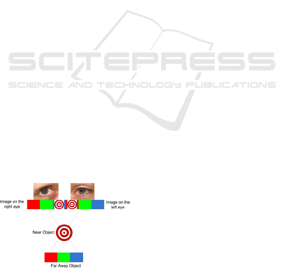
parallax effect (see Figure 1) is used to achieve
stereoscopic vision.
Figure 1: Illustration of the parallax effect for inducing
sensation of depth in the human brain (Andorko et al.,
2010).
The result is obtained by “tricking” the brain
causing it to gain depth perception (also known as
stereopsis). This means that bad quality stereoscopy
induces perceptual ambiguity in the viewer (Zeki,
2004). The reason for this phenomenon is that the
human brain is simultaneously more sensitive but
less tolerant to corrupt stereo images as well as
vertical shifts of both images, being more tolerant to
monoscopic images. Therefore, the brain does not
consent the differences between the images coming
from the left and right channels that are originated
from the two independent and optically unadjusted
cameras. A very interesting application for this type
of imaging technology is in the biomedical field.
Wireless capsule endoscopy, that take pictures along
the digestive system, present themselves as excellent
devices where to apply these image sensors
(Qureshi, 2004; Iddan et al., 2000), broadening the
possibilities of non-invasive examination methods.
Furthermore, the outspread of low-power small
dimensioned high-resolution cameras motivates
even more the fabrication of the next generation of
endoscopic swallowable pills. These capsules can be
electronically controlled for several purposes, from
guidance inside the digestive system to drug delivery
mechanisms. Presently, the capsules determine
where they are according to the pH levels in their
surroundings based on the different acidity profiles
across the digestive system. Another advantage of
the proposed imaging sensor is the compatibility
with the CMOS technology. Most notably, CMOS
allows the decrease of the power consumption and,
unlike the CCD technology, CMOS sensors can be
fabricated using the same manufacturing facilities as
the high-volume products of the semiconductor
114
P. Rocha R., P. Carmo J. and H. Correia J..
MICROLENSES FOR STEREOSCOPIC IMAGE FORMATION.
DOI: 10.5220/0003728901140118
In Proceedings of the International Conference on Biomedical Electronics and Devices (BIODEVICES-2012), pages 114-118
ISBN: 978-989-8425-91-1
Copyright
c
2012 SCITEPRESS (Science and Technology Publications, Lda.)
industry. Thus, CMOS microdevices are more
standardized and cost-effective to produce then the
CCDs microdevices. Considering the low-power
consumption of the CMOS microdevices, another
possibility that presents itself for the imaging
sensors is the integration of thin-films batteries with
silicon compatibility (Chan et al., 2008) and low
toxicity (Armand and Tarascon, 2008). The inherent
characteristics of the proposed imaging sensor
presented in this paper make it an interesting
solution for the capsule endoscopy integration
including the thin-films battery as the power source.
The fabrication of such a microdevice can be done
using the 0.7 µm CMOS process in the AMIS
foundry because it allows the production of both the
photodetectors and the read-out electronics within a
reasonable cost. Finally, since the aforementioned
process is very well characterized and known, the
time to manufacture the first working prototype is
expected to be short. This paper addresses on the
design and fabrication technology of the microlenses
for providing stereoscopic vision.
2 IMAGE SENSOR
ARCHITECTURE
The image sensor is composed by two pupils (two
entrance apertures just like the human eyes) from
where the left and right channels (the two POVs that
will originate the tridimensional effect) pass through
before being focused by an objective lens. This lens
focuses the two incident beams in the direction of
the microlens, where the light is concentrated in a
small sensitive area where the photodiodes are
placed. After passing through the optical filters, the
wavelengths coming from both the entrance
apertures are directed towards the respective CMOS
photodiodes. The two viewpoints are separated by
focusing each side onto the appropriate sensor
column under the microlens and optical filters.
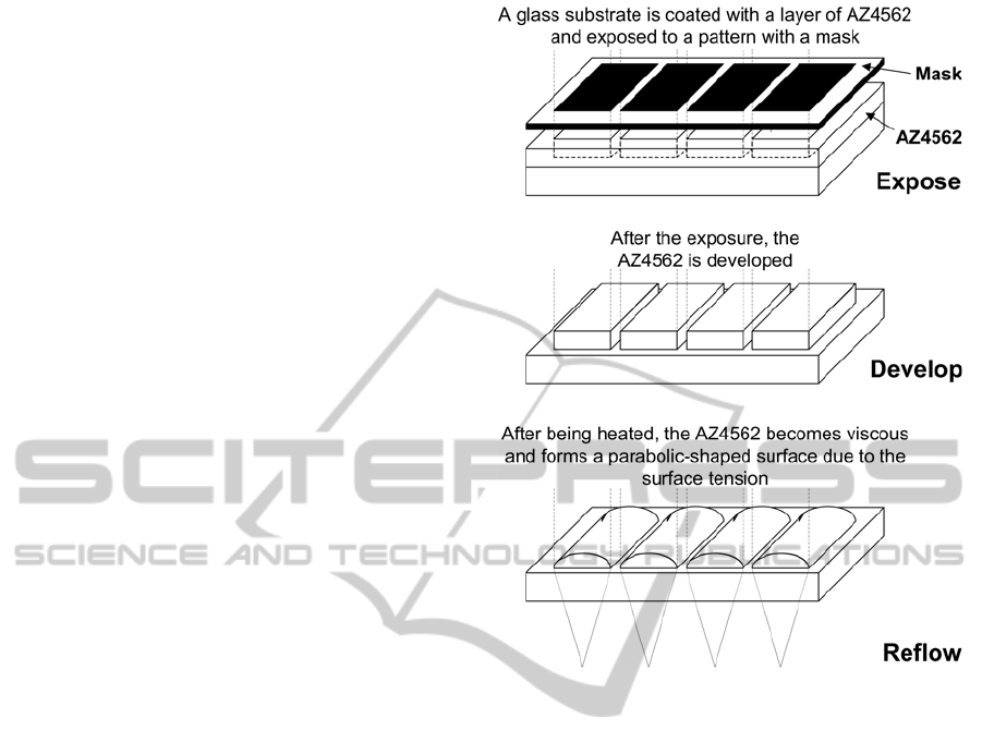
3 MICROLENSES FABRICATION
A. Microlens fabrication
There is a huge number of materials available for
fabricating microlenses arrays such as the SU-8/2,
AZ9260 and AZ4562, for example. These polymers
allow the microlens fabrication by thermally
reflowing the raw material, whose processing steps
Figure 2: The reflow process applied to the AZ4562
photoresist for fabricating microlenses arrays.
of the reflow process are presented in the Figure 2.
This permits the production of arrays containing a
million or more microlens of good optical quality in
just a few minutes and with high degree of
reproducibility of their characteristics. There are a
few geometrical parameters to take in account before
fabricating the microlenses. As depicted in Figure 3,
the paraxial focal length, f, of a microlens consisting
of a single spherical surface of radius R in a medium
of refractive index, n, is given by f=R/(n-1) and the
height, h, of the surface undulation of a microlens
with an aperture radius, r, is h=R-(R
2
-r
2
)
1/2
. The
volume of a cylinder of resist is Tπr
2
, where T is the
thickness before melting and the volume of the
microlens is 1/3πh
2
(3R-h). It therefore follows that
the necessary thickness is given by T=h/6×[3+(h/r)
2
].
The reflow process works well for microlenses of a
relatively high-numerical aperture (and low-focal
length, f), where the lens constitutes a significant
fraction of a hemisphere. This process is very tolerant
of the state of resist before melting, thus, acceptable
lenses can be made with aperture ratios between f/1
and f/3.
MICROLENSES FOR STEREOSCOPIC IMAGE FORMATION
115
f
h
R
Refraction index
n
Air
Microlens surface
Figure 3: Factors determining the focal length of
microlens.
Good-quality lenses are fabricated with relatively
crude lithography although greater consistency and
reliability is achieved only if the process is carried
out efficiently. The precise form of the microlenses,
and hence their focal properties, are determined by
the effects of the surface tension (Roulet et al.,
2001). In particular the contact angle of the softened
resist with the surface of the substrate will strongly
influence the shape of the microlens.
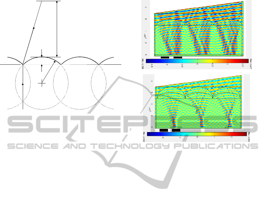
B. Microlens simulation
In Figure 4 it is possible to see the results of some
finite element method (FEM) simulations. These
simulations were performed considering the
impinging light with an angle of 7.6º degrees from
the left channel, but this methodology is also
applicable to the right channel and both channels
overlapping for the global effect. The dimensions of
the presented microlenses simulations have a W/L
ratio of 4.8 and 2.4 in (a) and (b), respectively. It is
clearly seen that the light concentrates in the
direction of the photodiodes represented as pairs of
black rectangles on the bottom of the figure. The
simulations also show that the best results, i.e. more
concentration of light, are achieved with microlenses
having a higher curvature. Moreover, another
important conclusion is shown, that it is possible to
separate the left and right channels for focusing the
specific wavelengths into the respective
photodiodes. This also allows estimating the cross-
talk between adjacent photodiodes, being smaller in
the micro lenses with higher curvature. It is assumed
in the simulations that the light had already passed
through the optical filters.
(a)
(b)
Figure 4: FEM simulations showing the light
concentration into the right photodiode. The simulations
where obtained respectively for lenses measuring with (a)
W/L=4.8 and (b) W/L=2.4. The simulations also allows to
roughly estimate the degree of cross talk between two
adjacent photodiodes (e.g., between the left and right
channels).
4 EXPERIMENTAL
C. Fabrication
The fabrication process of the microlenses array
requires several steps. First, it is necessary to deposit
the photoresist by means of a spin coater in a
previously cleaned substrate. To achieve the desired
thickness, the spin velocity is 6000 rpm and the time
will depend on the desired thickness. After the
coating, a prebake phase, using a computer
controlled hot plate at 100º C for 100 seconds, is
necessary to evaporate the solvents present in the
photoresist. This step is critical otherwise the resist
surface dries very fast and doesn’t allow the solvent
to exit the photoresist creating bubbles and possibly
the photoresist to lift. Next, to obtain the required
array-like structure, the mask with the correspondent
geometrical design is placed on top of the substrate
with the photoresist. This step serves for exposing
the PR to UV light, during 2 minutes, to make the
unexposed material insoluble. Afterwards, the
development phase, using the AZ 351B developer in
BIODEVICES 2012 - International Conference on Biomedical Electronics and Devices
116
a 1:4 concentration with distilled water, is required
to leave just the unexposed photoresist in the
substrate. To do this, the substrate is immersed in
the developer bath in a magnetic stirrer for 1 minute.
Finally, the structure is also placed in the hot plate
for a postbake phase at 115 º C for 100 seconds for
obtaining the final chemical stabilization and
substrate adhesion improvement. In order to obtain
the lens profile, a reflow technique is used. The
substrate with the PR array is placed at 180º C
during 10 hours.
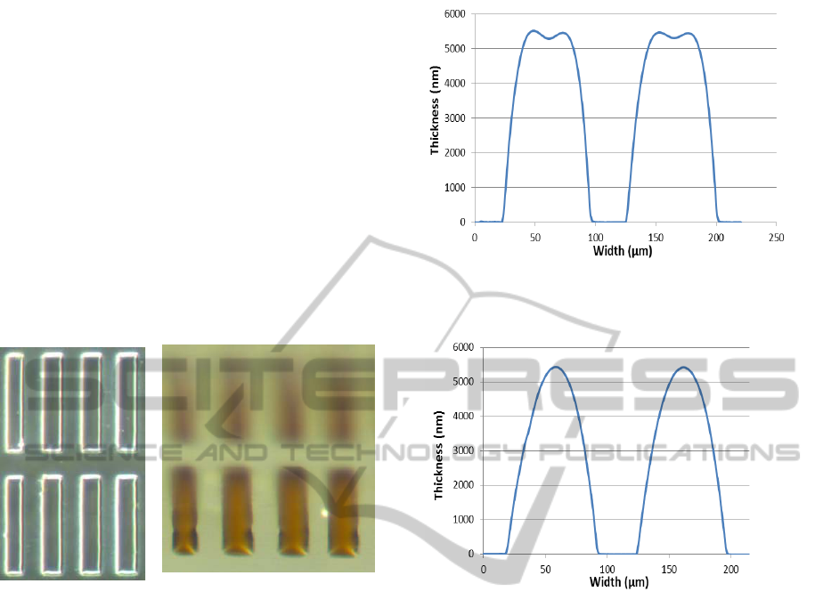
D. Characterization
In Figure 5, two photographs show the PR array
before and after the reflow step, respectively, on the
left, top view and on the right, tilted view.
Figure 5: (a) Figure 5: (b)
In Figures 6 (a) and (b) it is possible to see the
profiles of the PR before and after the reflow process
measured with a Veeco Dektak 150 profilometer.
This figure presents the typical initial profile
seen during the fabrication of microlenses using PR
(Emadi et al., 2009; O’Neill et al., 2002). After
applying a temperature higher than the glass
transition temperature of the PR, the viscosity
decreases and the consequent flow due to surface
tension occurs. These structures are the first
prototypes built using photolithography but the final
size of the microlenses can be further reduced using
a chromium-on-glass mask. Nevertheless, it is clear
from the previous figures that the thermal reflow
process permitted obtaining the desired microlens
profile to concentrate the light into specific
directions.
Figure 6 (a): Profile of the PR array before the thermal
reflow
.
Figure 6 (b): Profile of the microlenses obtained after the
thermal reflow step.
5 CONCLUSIONS
This paper presented a microlenses fabrication
process for integration on a stereoscopic image
sensor in CMOS technology for use in biomedical
devices. The microlenses design started with the
FEM simulations to set some parameters needed to
fulfill the desired objectives. These objectives
included the microlenses’ W/L dimensional ratio of
4.8 and 2.4 because of the size and pitch of the
photodetectors. Each photodetector measures a
specific wavelength with is difracted by the
microlenses. The complete fabrication process was
explained and the initial and final structures obtained
were physically characterized. It was shown that the
reflow step is what determines the actual
microlenses profile. The several steps that comprise
the photolithographic fabrication process were done
for a first prototype but smaller ones are already
being developed and tested using a chromium-on-
glass mask and a mask aligner as the UV light
MICROLENSES FOR STEREOSCOPIC IMAGE FORMATION
117

source. The integration of such stereoscopic imaging
sensor in a biodevice such as an endoscopic capsule
for non-invasive examination of the digestive system
is a very appealing solution for the presented
fabrication technology.
ACKNOWLEDGEMENTS
This work was fully supported by the Portuguese
Foundation for Science and Technology under the
project FCT/PTDC/EEA-ELC/109936/2009.
REFERENCES
I. Andorko, et al., "Hardware implementation of a real-
time 3D video acquisition system", in proc. of 12th
International Conference on Optimization of Electrical
and Electronic Equipment (OPTIM 2010), Brasov,
Ronaia, 20-22 May, pp. 920-925.
S. Zeki, "The neurology of ambiguity", Consciousness and
Cognition, Vol. 13, pp. 173-196, 2004.
W. Qureshi, "Current and future applications of the
capsule camera", Nature Reviews Drug Discovery,
Vol. 3, pp. 447-480, May 2004.
G. Iddan, et al, "Wireless capsule endoscopy", Nature,
Vol. 405, pg. 417, May 2000.
C. K. Chan, et al, "High-performance lithium battery
anodes using silicon nanowires", Nature, Vol. 3, pp.
31-35, January 2008.
M. Armand, M. Tarascon, "Building better batteries",
Nature, Vol. 451, pp. 652-657, February 2008.
J-C. Roulet, et al, “Fabrication of Multilayer Systems
Combining Microfluidic and Microoptical Elements
for Fluorescence Detection”, Journal of
Microelectromechanical systems, Vol. 10, No. 4,
December 2001.
A Emadi, et al, “Vertically tapered layers for optical
applications fabricated using resist reflow”, J.
Micromech. Microeng., 19, 2009.
F. O’Neill, et al, “Photoresist reflow method of microlens
production Part I: Background and experiments”,
Optik 113, No. 9, pp. 391-404, 2002
BIODEVICES 2012 - International Conference on Biomedical Electronics and Devices
118
