
A FRONT-END STAGE FOR NEURAL SIGNAL RECORDING
BASED ON A SIGMA-DELTA MODULATOR
Caterina Carboni, Daniela Loi and Massimo Barbaro
Dept. of Electrical and Electronic Engineering, University of Cagliari, Cagliari, Italy
Keywords:
Neural signal recording, Low noise amplifier.
Abstract:
A new device for peripheral neural signals recording is presented. The designed system is composed by an
analog and a digital part. The analog part, to be integrated on an implantable CMOS chip, is kept as simple
as possible and hosts a low noise first order pre-amplifier/pre-filtering stage that provides a 46dB gain in the
bandwidth 800Hz − 7.2kHz and a 16-bit 3rd order sigma delta modulator. A highly selective band-pass filter
is implemented into the digital domain, incorporated in the decimator block of the sigma-delta converter; in
this way it is possible to reduce total area (which is 0.4mm
2
for a single input channel) and power consumption
(250µW , single channel) in the integrated, implantable module. Simulation results prove the capability of the
proposed system to record signals whose magnitude is in the order of tens of microvolts thanks to the low
Input Referred Noise (IRN) of 2.4µV
rms
of the input stage.
1 INTRODUCTION
In the last decades, research on biomedical engineer-
ing has been widely propelled by many groups with
the aim to find a solution for a number of diseases
and to grant a better quality of life to patients. One of
the topics that has been subject to a great attention is
the interface between the human nervous system and
the machines (BMI). Such studies have a wide range
of potential applications: from diseases affecting the
nervous systems (like Parkinson, epilepsy, multiple
sclerosis) to treatment of permanent damages of the
spinal cord and, finally, prosthetics (Pereira et al.,
2007; Liu et al., 2000; Von Arx and Najafi, 1999).
This work is included in the latter field: our aim, in
fact, is to develop a system capable to record the sig-
nals captured by an electrode inserted in the periph-
eral nervous system of an amputee patient and exploit
them to drive a robotic limb. With this approach, there
are several advantages with respect to the more tra-
ditional Electromyographic (EMG) prostheses. First,
the limb will be controlled using the thought, thus al-
lowing the patient to feel the prosthetic arm as a nat-
ural extension of his/her body. Secondly, the inser-
tion of the electrode inside the nerves makes it possi-
ble to restore the sensory feedback, providing current
pulses whose shape, frequency and amplitude can be
programmed according to stimuli coming by temper-
ature and pressure sensors collocated on the robotic
limb (Micera et al., 2010; Dhillon and Horch, 2005).
The main problem, in this kind of application, is the
weak amplitude of the extracellular nervous signals
that can span in a range from few microvolts to 500
microvolts (Harrison and Charles, 2003; Yoshida and
Stein, 1999; Loi et al., 2011). Moreover, such sig-
nals are drowned in a noisy environment mainly due
to electromyographic (EMG) interferences from the
muscle fascicles surrounding the nerves; EMG sig-
nals are in the order of magnitude of millivolts, thus
several times the amplitude of the neural signals. Fur-
thermore, power spectral densities (PSD) of the in-
terferences and of the useful signal are very close and
partially overlap (Rieger et al., 2003; Harrison, 2007).
In this context, it is mandatory to properly amplify
the weak useful signal and to filter out the huge noise
component. Given the partial overlap of the PSDs, a
highly selective filter is needed to reject most of the
interferences. The implementation of such a circuit in
the analog domain is possible and it is a widely used
approach (Guo et al., 2004; Lee and Lee, 2005; Lim-
nuson et al., 2009), but it implies a number of prob-
lems in the design: highly selective filters are prone
to instability and cascading many amplifiers is power
consuming. Such problems make the implementation
of an integrated device for chronicle implants diffi-
cult. In our approach, we propose to adopt a sigma-
delta architecture which is capable to shift most of the
complexity of the realization either of the highly se-
207
Carboni C., Loi D. and Barbaro M..
A FRONT-END STAGE FOR NEURAL SIGNAL RECORDING BASED ON A SIGMA-DELTA MODULATOR.
DOI: 10.5220/0003782802070212
In Proceedings of the International Conference on Biomedical Electronics and Devices (BIODEVICES-2012), pages 207-212
ISBN: 978-989-8425-91-1
Copyright
c
2012 SCITEPRESS (Science and Technology Publications, Lda.)
lective filter and of the analog-to-digital conversion in
the digital domain thus keeping only a small analog
circuitry in the implantable chip. In this way a more
robust and noise immune system can be designed with
a lower power consumption. The device is therefore
made up of two modules: an implantable integrated
circuit and an external board. The microchip hosts
only a first-order pre-amplifier/pre-filtering stage and
the sigma delta modulator (each of which for every
input channel) while the highly selective filter is im-
plemented altogether with the decimator on the exter-
nal digital platform. In this paper we present the de-
sign and the simulation results concerning the analog
part of the recording path. In section 2 we present the
architecture of the whole system, while in sections 3
and 4 we report the design choices respectively for
the pre-amplifier/pre-filtering block and for the delta-
sigma modulator. Simulation results are provided in
section 5.1 and conclusions are drawn in section 6.
2 SYSTEM ARCHITECTURE
The block diagram in Fig. 1 shows the system archi-
tecture which is composed by two main blocks: the
analog front/end and the digital processing unit. The
analog module was designed in a 0.35µm CMOS pro-
cess from AMS (Austriamicrosystems) with double-
poly capacitors, 3.3V power supply and 4 metal lay-
ers. Area and power constraints are particularly com-
pelling since the chip must be integrated with the elec-
trode and implanted in the patient stump. The front-
end module works in a bidirectional way, it imple-
ments basic signal conditioning on the incoming neu-
ral signal (in recording mode) and provides current
pulses on the feedback path (in stimulation mode).
The signal is, thus, filtered and amplified by the Pre-
Filtering/Pre-amplifier block as close as possible to
the recording site. In this way, the noise due to long
cables and connection paths can be avoided. The con-
ditioned signal is then converted into a 1-bit digital
stream by the delta-sigma modulator and sent to the
digital module for decimation and further processing.
One of such signal’s streams is needed for each input
channel if the device is connected to a multichannel
electrode. The digital module is hosted on an exter-
nal board; it implements the decimation block of the
sigma-delta converter altogether with the highly se-
lective bandpass filter. The digital module is also re-
sponsible of the generation of digital programmable
stimulation waveforms and of management of the
communication between the artificial limb and the
electrodes. The digital unit will be implemented on
programmable logic (FPGA), hosted on the robotic
limb. A further advantage of such approach, is the
possibility of changing the selectivity of the filter on
the fly by adjusting the digital parameters.
Pre
-
ampli
Pre-filtering
Implantable CMOS circuit
Electrodes
Current DAC for
stimulation
ΣΔ
modulator
ΣΔ
decimator
Digital
patterns
generation
Digital System
Controller on
FPGA
Figure 1: Block diagram of the recording and stimulation
system.
3 PRE-AMPLIFIER AND
PRE-FILTERING
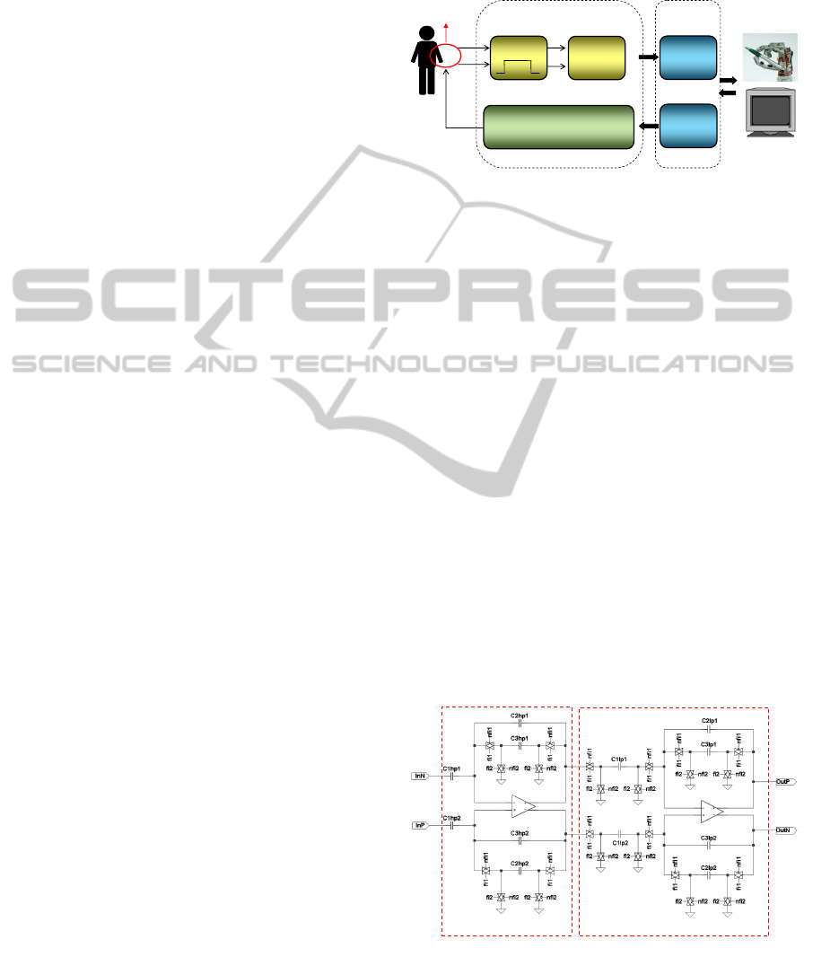
Fig. 2 shows the pre-amplifier/pre-filtering block that
was implemented with a first order switched capaci-
tor (SC) filter. SC-filters have, in fact, the great ad-
vantage, over their continuous-time counterpart, to
achieve a better precision in the cut-off frequency im-
plementation. The Bandpass Filter (BPF) was real-
ized cascading a Highpass filter (HPF) with a Low-
pass Filter (LPF); the HPF is used as first stage in or-
der to start rejecting the EMG interferences as close
as possible to the electrode, before any amplifica-
tion. The filter specifications required a bandwidth
between 800Hz and 8kHz and a gain of 200V /V . This
gain value has been determined to maximize the am-
plification at neural frequencies avoiding the risk of
amplifier saturation. In Table 1 the values used for
the filter capacitance are summarized.
HPF
L
PF
Figure 2: Band-Pass filter.
The switches were realized using transmission
gates at minimum size in order to reduce area. A
BIODEVICES 2012 - International Conference on Biomedical Electronics and Devices
208
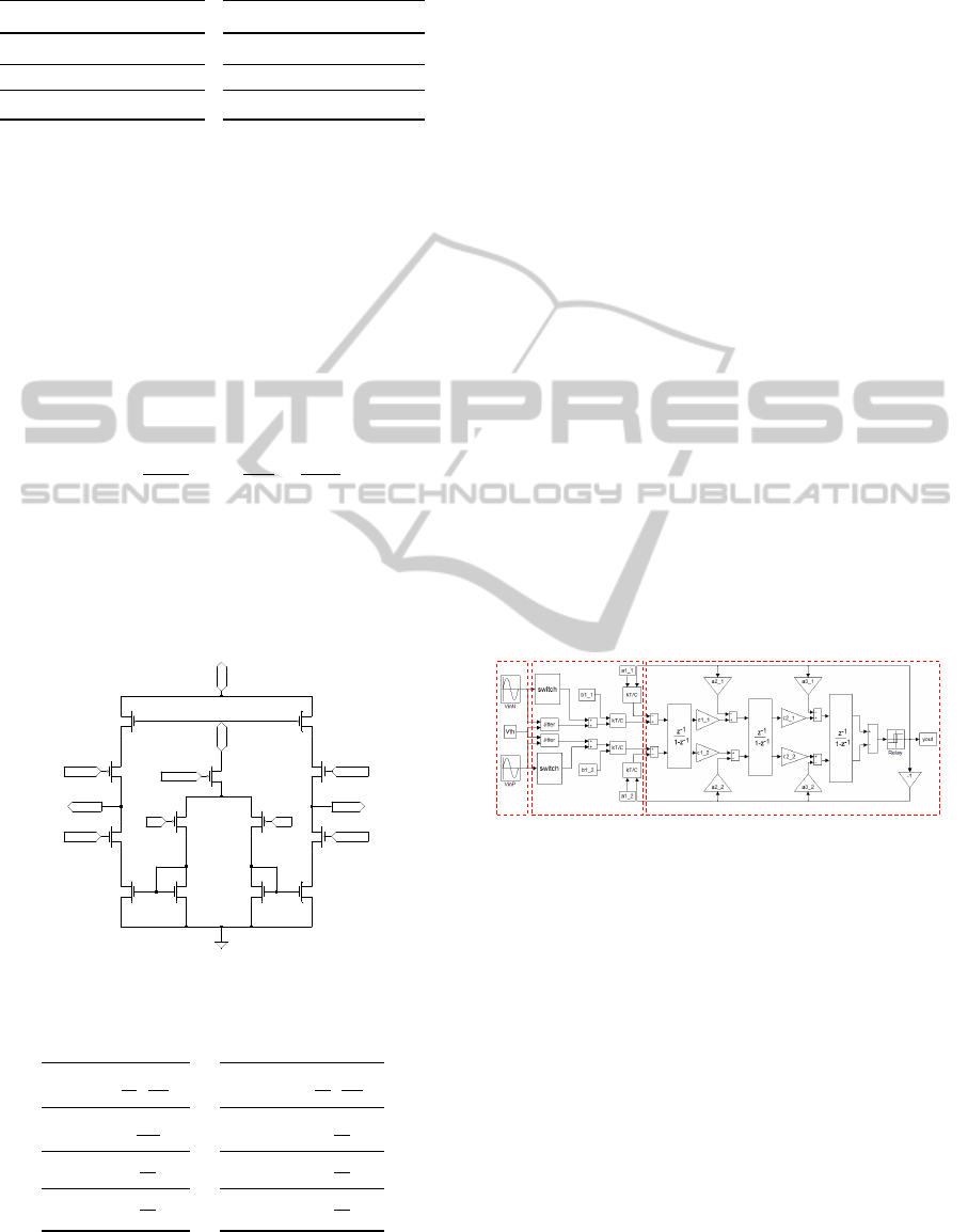
Table 1: Filter Capacitance values.
C Value [pF]
C
1hp1,2
80
C
2hp1,2
13
C
3hp1,2
1.7
C Value [pF]
C
1l p1,2
10
C
2l p1,2
1.6
C
3l p1,2
2
simple cascode symmetrical OTA (Fig. 3) was cho-
sen for the operational amplifier implementation and
it was carefully dimensioned in order to minimize the
Input Referred Noise (IRN). Flicker noise is one of
the major concerns, given the low frequencies of the
neural signal, thus a p-type differential pair with large
area was adopted to minimize this contribute (Razavi,
2001). Thermal noise was addressed using a large g
m
for the differential pair and reducing the g
m
of the out-
put branch transistor (Harrison and Charles, 2003) ac-
cording to the formula:
v
n,th
=
16kT
3g
m1
(
1 +
g
m6
g
m1
+
g
m12
g
m1
)
where k is the Boltzmann constant, T the absolute
temperature and g
mx
the transconductance of transis-
tor x. In Table 2 all sizes are reported, all transistors
were biased with a 4µA current. A passive SC com-
mon mode feedback block was used for power saving.
M3 M6
M8
M4M5
M7
M1
M9
M12
M10
M11
M2
M13
VddVdd
Vn Vp
Vbiasp
Vcasp
VcasnVcasn
Vcasp
Vctrl
VoutpVoutn
Figure 3: Symmetrical OTA.
Table 2: OTA dimensions.
W
L
[
µ
µ
µm
µ
µ
µm
]
M
1,2
800
10
M
3,4
5
20
M
5,6
5
20
W
L
[
µ
µ
µm
µ
µ
µm
]
M
7,8
15
20
M
9,10
15
20
M
11,12
5
20
4 SIGMA-DELTA MODULATOR
Once that the useful signal has been properly am-
plified it is possible to convert it in the digital do-
main. With this purpose, a third order switched ca-
pacitor sigma-delta modulator in a Cascade of Inte-
grators with FeedBack (CIFB) configuration was de-
signed. The weakness of the neural signals required
to adopt a 16-bit converter; with a reference voltage
of V
re f
= 2V
pp
, a LSB = 0.15µV can be achieved, al-
lowing the detection of microvolt level signals. This
result was achieved using an OSR = 128 with a sam-
pling frequency f
s
= 2.048MHz. Due to long simu-
lation time, preliminary tests were performed using a
behavioral model in Simulink environment and, only
once that the specifications were satisfied, the circuit
was implemented at transistor level.
4.1 Behavioural Simulink Model
A Simulink model has great advantages in terms of
simulation time saving moreover, it allows the intro-
duction of blocks modelling noise sources and opamp
non-idealities thus granting an excellent reliability of
the system and a good agreement with transistor level
simulations. Fig. 4 shows the diagram block used for
this purpose.
inputs
noise sources
3° order ΣΔ modulator
Figure 4: Sigma-delta modulator: behavioural Simulink
model.
The model is a modification of what presented
in (Malcovati et al., 2003) and (Zare-Hoseini et al.,
2005) which take into consideration saturation, slew
rate, finite gain and bandwidth limitations. KT /C
noise, thermal noise of the amplifier, switches non-
idealities and clock jitter effects have also been in-
cluded. With respect to the original model our system
was transformed in a fully differential architecture in
order to make it more similar to the actual transis-
tor implementation (shown in the following subsec-
tion). The coefficients (summarized in in Table 3)
were chosen using the Schreier Toolbox (Schreier and
Gabor C., 2001) with a 18-bits target resolution (we
added 2 bits for noise margin).
The mismatch effects were also taken into con-
sideration since the coefficients have been generated
A FRONT-END STAGE FOR NEURAL SIGNAL RECORDING BASED ON A SIGMA-DELTA MODULATOR
209
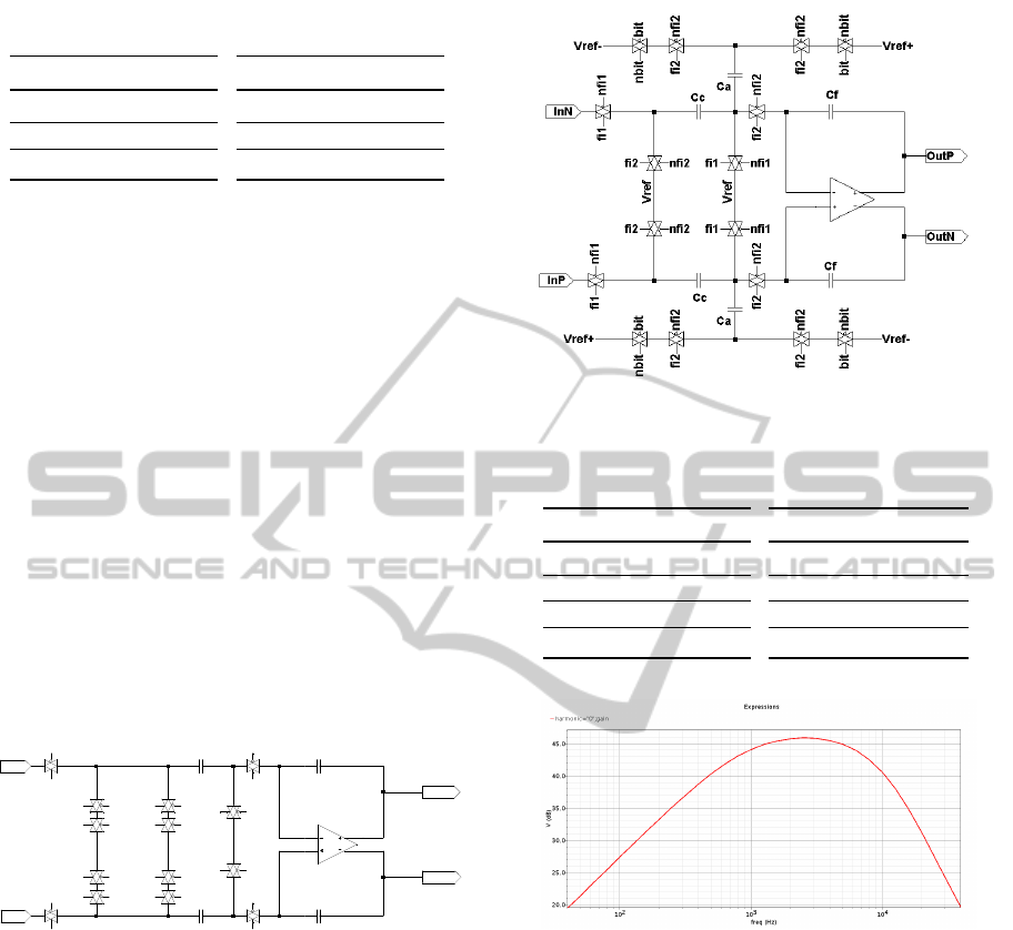
Table 3: Sigma delta modulator: coefficients.
Coefficient Value
a
1
0.05
a
2
0.3
a
3
0.8
Coefficient Value
b
1
0.05
c
1
1
c
2
1
as capacitor ratios, whose values have been extracted
randomly from a normal distribution within a 6σ
range around the nominal value.
4.2 Transistor Level Design
The block diagram described in the previous section
was mapped into a transistor level design using a
SC circuit. The main components are the discrete
time integrators shown in Fig. 5 (first stage) and
Fig. 6 (second and third stages). It can be observed
that all the feedback paths have been realized driv-
ing a switch with the quantizer output and connecting
the corresponding capacitor to the reference voltages
V
re f −
= V
dd
/2 − 1 and V
re f +
= V
dd
/2 + 1. Since the
a and b coefficients are equals, in the first stage the
same capacitor was shared for the two paths while
in the second and third stage two different capacitors
were used in order to implement coefficients a and c.
Cab
Cab
Cf
Cf
InN
InP
fi1
fi2
nfi1
nfi2
fi2
fi1
fi1
fi2
nfi1
nfi2
fi1
nfi2
nfi1
nfi1
OutP
OutN
fi2 nfi2
nbit bit bit nbit
Vref-
Vref+
bitbit nbitnbit
fi2 nfi2fi2nfi2
Vref
Figure 5: Sigma-delta modulator: first integrator schematic.
In Table 4 all the values used for the capacitors
are reported, each coefficient can be obtained by ca-
pacitance ratios using the relationship x = C
x
/C
f
. A
simple symmetrical OTA was used to realize the oper-
ational amplifier, it has been sized in order to meet the
specifications determined with the behavioral simula-
tion (in terms of DC gain, GBW, dynamic range and
slew rate). The single bit quantizer has been designed
with a track and latch circuit.
Figure 6: Sigma-delta modulator: second and third integra-
tor schematic.
Table 4: Sigma-Delta modulator: capacitance values.
C Value [pF]
C
ab,1st
0.2
C
f ,1st
4
C
a,2st
1.2
C
c,2st
4
C Value [pF]
C
f ,2st
4
C
a,3st
3.2
C
c,3st
4
C
f ,3st
4
Figure 7: Bandpass filter: Frequency response.
5 SIMULATION RESULTS
5.1 Pre-amplifier/Pre-filter Results
The frequency response of the operational amplifier
of Fig. 3 shows a DC-gain of 108dB with a GBW =
1MHz, the 62
o
phase margin ensures a good com-
promise between ringing avoidance and settling time.
The integrated input referred noise in the bandwidth
800Hz − 8kHz is 2.1µV
rms
allowing to detect signals
in the order of magnitude of tens of microvolts. The
bandpass filter provides a gain of 46dB within the 3dB
bandwidth 800Hz − 7.2kHz (Fig. 7) and the simu-
lated noise in this bandwidth is 2.4µV
rms
. The gain
BIODEVICES 2012 - International Conference on Biomedical Electronics and Devices
210
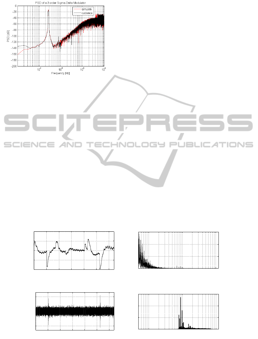
Figure 8: Sigma-Delta modulator PSD: behavioral sim-
ulation (red curve) and transistor level simulation (black
curve).
value was chosen to avoid the risk of saturation due
to EMG interferences. We considered a worst condi-
tion of a 10mV interference at 300Hz. In this case, the
gain at 300Hz is 65V /V thus the residual EMG signal
at the output of the filter will be 650mV
pp
, far away
to rich the saturation limit of 2V
pp
of the sigma-delta
modulator. This residual out of band huge interfer-
ence will be completely rejected in the digital domain
by the high-selective band pass decimator.
5.2 Sigma-delta Modulator Results
The power spectral density (PSD) of the sigma-delta
modulator, is shown in Fig. 8: the red curve rep-
resents the results obtained by Simulink simulations
while the black one is the PSD extracted by the tran-
sistor level simulation performed with Cadence. As
it can be observed, the two curves are very simi-
lar each other, confirming the good agreement be-
tween the two models. The final resolution achieved
is 16.12bit corresponding to a SNR = 98.8dB with
an OSR = 128. The system functionalities have been
tested using, as modulator input, pre-recorded neu-
ral patterns, on the basis of recordings made in clini-
cal trials with rabbits. The input pattern, represented
in Fig. 9(a), corresponds to 3.2 seconds of record-
ing during which the rabbit was subjected to vibra-
tions at 50Hz and 100Hz in cutaneous afferents. The
input signal is affected by EMG and ECG interfer-
ences with a very large amplitude (in the millivolts
range) and a spectrum (Fig. 9(b)) concentrated be-
low 300Hz. Such interferences completely mask the
underlying neural content. The signal has been pro-
cessed by the delta-sigma modulator and then deci-
mated and band-pass filtered using a digital filter in
simulink environment. Fig. 9(c) displays the input-
referred output signal and Fig. 9(d) its power spec-
tral density: the low-frequency interferences are com-
pletely removed and the weak neural signal (in the mi-
crovolts range) is now visible, as well as its frequency
signature. In Table 5 the main characteristics of the
system are summarized.
6 CONCLUSIONS
A bio-electronic interface for peripheral neural signal
recording was designed. The first stage is composed
by a first order pre-amplifier and pre-filtering block
0 0.5 1 1.5 2 2.5 3
−2
−1
0
1
2
Time (s)
Amplitude (mV)
(a) Input Signal.
10
2
10
3
10
4
0
20
40
60
Frequency (Hz)
Amplitide (mV
2
)
(b) Input Spectrum.
0 0.5 1 1.5 2 2.5 3
−100
0
100
Time (s)
Amplitude (µV)
(c) Output Signal.
10
2
10
3
10
4
0
2
4
6
Frequency (Hz)
Amplitude (mV
2
)
(d) Output Spectrum.
Figure 9: Sigma Delta modulator: pre-recorded neural signal processing.
A FRONT-END STAGE FOR NEURAL SIGNAL RECORDING BASED ON A SIGMA-DELTA MODULATOR
211

Table 5: Main parameters summary. Data are referred to
each input channel.
parameter value
Gain 46dB
f
L
, f
H
800Hz, 7.2kHz
Power 250µW
Area 0.4mm
2
IRN 2.4µV
rms
resolution 16.12bit
that provides a gain of 200V /V in the bandwidth
range 800HZ − 7.2kHz. The signal is then converted
in the digital domain by a 16-bit sigma delta modula-
tor and transmitted to the digital part of the system for
decimation, highly selective band-pass filtering and
further signal processing. The analog front-end of the
designed system (prefiltering/preamplifier and sigma-
delta modulator) exhibits a total area of 0.4mm
2
with
a 240µV power consumption (for each input channel).
Simulation results show that the system is capable
to record a neural signal in the order of magnitude
of tens of microvolts thanks to its low IRN equal to
2.4µV
rms
.
ACKNOWLEDGEMENTS
The work described was supported by MIUR (Ital-
ian Ministry of Education, University and Research)
through project Openhand (PRIN 2008). The au-
thors wish to thank Laura Muggianu for helping with
the design and simulations and Silvestro Micera of
Scuola Superiore Sant’Anna di Pisa (SSSA) for neu-
ral traces providing.
REFERENCES
Dhillon, G. S. and Horch, K. W. (2005). Direct neural sen-
sory feedback and control of a prosthetic arm. IEEE
Trans. on Neural Systems and Rehabilitation Engi-
neering, pages 468–472.
Guo, H., Champion, C., Rector, D. M., and La Rue, G.
(2004). A low-power low-noise sensor ic. 2004
IEEE Workshop on Microelectronics and Electronic
Devices, pages 60–63.
Harrison, R. R. (2007). A versatile integrated circuit for the
acquisition of biopotentials. Custom Integrated Cir-
cuits Conference, pages 115–122.
Harrison, R. R. and Charles, C. (2003). A low-power
low-noise cmos amplifier for neural recording appli-
cations. IEEE Journal of Solid-State Circuits, 38:958–
965.
Lee, S. Y. and Lee, S. C. (2005). An implantable wireless
bidirectional communication microstimulator for neu-
romuscolar stimulation. IEEE Trans. Circuit System,
52:2526–2538.
Limnuson, K., Tyler, D. J., and Mohseni, P. (2009). Inte-
grated electronics for peripheral nerve recording and
signal processing. 31st Annual International Confer-
ence of the IEEE EMBS, pages 1639–1642.
Liu, W., Vichienchom, K., Clements, M., DeMarco, S.,
Hughes, C., McGucken, E., Humayun, M., De Juan,
E., Weiland, J., and Greenberg, R. (2000). A neuro-
stimulus chip with telemetry unit for retinal pros-
thetic device. IEEE Journal of Solid-State Circuits,
35:1487–1497.
Loi, D., Carboni, C., Angius, G., Angotzi, G., Barbaro, M.,
Raffo, L., Raspopovic, S., and Navarro, X. (2011). Pe-
ripheral neural activity recording and stimulation sys-
tem. IEEE Trans. Biomedical Circuit System, 5:368–
379.
Malcovati, P., Brigati, S., Francesconi, F., Maloberti, F.,
Cusinato, P., and Baschirotto, A. (2003). Behavioral
modeling of switched-capacitor sigmadelta modula-
tors. IEEE Trans. on Circuits and Systems-I, 5:352–
364.
Micera, S., Citi, L., Rigosa, J., Carpaneto, J., Raspopovic,
S., Di Pino, G., Rossini, L., Yoshida, K., Denaro, L.,
Dario, P., and Rossini, P. M. (2010). Decoding infor-
mation from neural signals recorded using intraneu-
ral electrodes: Toward the development of a neuro-
controlled hand prosthesis. Proceedings of the IEEE,
98(3):407–417.
Pereira, E., Green, A., and Nandi, D. (2007). Deep brain
stimulation: indications and evidence. Expert Rev
Med Devices, 4:591–603.
Razavi, B. (2001). Design of analog cmos integrated cir-
cuits. McGRAW HILL International Edition.
Rieger, R., Taylor, J., Demosthenous, A., Donaldson, N.,
and Langlois, P. J. (2003). Design of a low-noise
preamplifier for nerve cuff electrode recording. IEEE
Journal of Solid-State Circuits, 38(8):1373–1379.
Schreier, R. and Gabor C., T. (2001). Understand-
ing delta-sigma data converters. IEEE Press/Wiley-
Interscience.
Von Arx, J. and Najafi, K. (1999). A wireless single-chip
telemetry-powered neural stimulation system. IEEE
Journal of Solid-State Circuits, pages 214–215.
Yoshida, K. and Stein, R. B. (1999). Characterization of
signals and noise rejection with bipolar longitudinal
intrafascicular electrodes. IEEE Trans Biomed Eng,
46:226–234.
Zare-Hoseini, H., Kale, I., and Shoaei, O. (2005). Mod-
eling of switched-capacitor deltasigma modulators in
simulink. IEEE Trans. on Instrumental and Measure-
ment, 54:1646–1654.
BIODEVICES 2012 - International Conference on Biomedical Electronics and Devices
212
