
SURFACE PASSIVATION EFFECT IN SGOI NANOWIRE
BIOSENSOR WITH HIGH GE FRACTION
Kow-Ming Chang
1,2
, Chu-Feng Chen
1
, Chiung-Hui Lai
3
, Cheng-Ting Hsieh
1
, Chin-Ning Wu
1
,
Yu-Bin Wang
1
, Chung-Hsien Liu
1
and Kuo Chin Chang
4
1
Dept. of Elec. Engineering and Inst. of Elec., National Chiao-Tung University, No. 1001
University Rd., Hsinchu 300, Taiwan, R.O.C.
2
Department of Electronic Engineering, I-Shou University, No.1, Sec. 1, Syuecheng Rd., Kaohsiung 840, Taiwan, R.O.C.
3
Dept. of Electronics Engineering, Chung Hua University, No. 707, Sec.2, WuFu Rd., Hsinchu, 300, Taiwan, R.O.C.
4
Dept. MD Tse-An Clinic 319, Chung Cheng Rd., Tse Kuan District, Kaohsiung City, Taiwan, R.O.C.
Keywords: SiGe-on-insulator, Biosensor, Passivation, Sensitivity.
Abstract: The increase of surface to volume ratio results in the enhancement of the sensitivity of the nanowires. Our
previous studies have shown that the higher Ge fraction of Si
1-x
Ge
x
nano-wire improves the sensitivity of
the nanowire biosensor as a result of carrier mobility enhancement in strain-Si. Increasing the fraction of Ge
in SiGe-on-Insulator (SGOI) using Ge condensation by oxidation has obtained a significant enhancement in
hole mobility, further improving the sensitivity of SGOI nanowire. However, the sensitivity of SGOI
nanowire was degraded for exceeding a Ge fraction of 20% (i.e., high Ge fraction), resulting from the
unstable surface state. In this work, a top surface passivation SiO
2
layer was deposited on Si
0.8
Ge
0.2
nanowire and the sensitivity was about 1.3 times greater than nanowire sample without the top passivation
layer.
1 INTRODUCTION
The sensitivity of SGOI can be enhanced by
increasing the surface to volume ratio to condense
carriers in very thin conductivity layer. The
conduction is modified by the surface charges that
surround the nanowire surface (Li, 2005). In our
previous studies, the higher surface to volume ratio
was achieved by utilizing SiGe/a-Si stacking
structure (Chang, 2011). Moreover, an increase of a
Ge fraction of Si
1-x
Ge
x
improves the nanowire
biosensor sensitivity due to higher carrier mobility
(Chang, 2008). Ultrathin SGOI with high Ge
fraction was fabricated by utilizing Ge condensation
and Ge piling up at the SiO
2
/SiGe interface by
oxidation. However, the higher interface trap density
at the SiO
2
/SiGe interfaces was about 10
-12
cm
-2
after
oxidation (LeGoues, 1989). Besides, an unstable
surface state of semiconductor with free surface
which caused by a lot of dangling bond at free
surface and higher Ge fraction of Si
1-x
Ge has higher
surface state and results in fast oxidation rate
(Tanaka, 2008). Fast oxidation rate can create more
unstable surface state (Yang, 2008).To reduce
unstable surface state, a SiO
2
passivation layer is
introduced to suppress surface state less than 10
11
cm
-2
eV
-1
.The surface state of free surface is around
10
15
cm
-2
eV
-1
. In this work, SiO
2
layer is selected as
passivation layer to improve interface state and O
2
gas buffer layer to reduce oxidation rate for 20% Ge
fraction of SiGe nanowire sensors.
2 EXPERIMENT
An a-Si/Si
1-x
Ge
x
was deposited on the patterned 300-
nm-hight bottom oxide. The deposition thickness of
a-Si is 200Å, and Ge fraction of Si
1-x
Ge
x
splits in
this experiment is 7, 14, and 20 %, respectively. To
clarify the influence of passivation layer on the
nanowire sensitivity, nanowire sensors with and
without the passivation SiO
2
layer were fabricated.
The passivation SiO
2
was split in two thicknesses,
100 and 200 Å. The poly-Si nanowire was also
fabricated as control group to verify oxidation rate.
After the a-Si/SiGe layer formation, the samples
384
Chang K., Chen C., Lai C., Hsieh C., Wu C., Wang Y., Liu C. and Chang K..
SURFACE PASSIVATION EFFECT IN SGOI NANOWIRE BIOSENSOR WITH HIGH GE FRACTION.
DOI: 10.5220/0003875403840387
In Proceedings of the International Conference on Biomedical Electronics and Devices (BIODEVICES-2012), pages 384-387
ISBN: 978-989-8425-91-1
Copyright
c
2012 SCITEPRESS (Science and Technology Publications, Lda.)
annealed in O
2
gas mixed with 13% N
2
gas ratio at
950
o
C for 180 sec, followed by the thermal
evaporation of Al films and the definition of the
electrodes by the mask process. The poly-Si and
SiGe nanowires were implanted in p-type nanowire.
To functionalize a-Si/Si
1-x
Ge
x
nanowires, the wires
were adopted the 3-aminopropyltri-ethoxysilance
(APTES) to modify the surface of the silicon oxide
around the nanowires. A hydroxyl functional group
on the surface of the oxide was replaced by methoxy
groups of APTES modules, and simultaneously, the
surface of the nanowire was terminated by amine
groups. From our earlier investigations (Chang,
2008), the amine groups were prone to deplete
positive carriers, reducing the conductivity of the p-
type nanowire. Next, bis (3-sulfo-N-
hydroxysuccinimide ester) sodium salt (BS3) was
used as a linker between APTES and IgG antibody.
BS3 was prone to becoming negatively charged,
increasing the conductivity of the p-type nanowire
because of the accumulation of the holes on the
surface of the nanowire.
The Hewlett Packard HP 4156A was used in this
study to measure the electric characteristics of
nanowire sensor. Drain voltage (V
D
) was varied
from -10 to 10V and 500 mV a step, and back gate
voltage was 0 V. The measurement of electric
characteristics was performed at every stage of
surface modification, and the average conductance
was then extracted from I
D
-V
D
characteristics with
V
D
= 3~6 V. The sensitivity (S) of a nanowire-based
sensor is defined as the ratio of the magnitude of
conductance change to the baseline conductance
value:
00
0
G
G
G
GG
S
(1)
where G
0
is the conductance before molecule
capture, G is the conductance after molecule capture,
and G is the different between G and G
0
.
3 RESULTS AND DISCUSSIONS
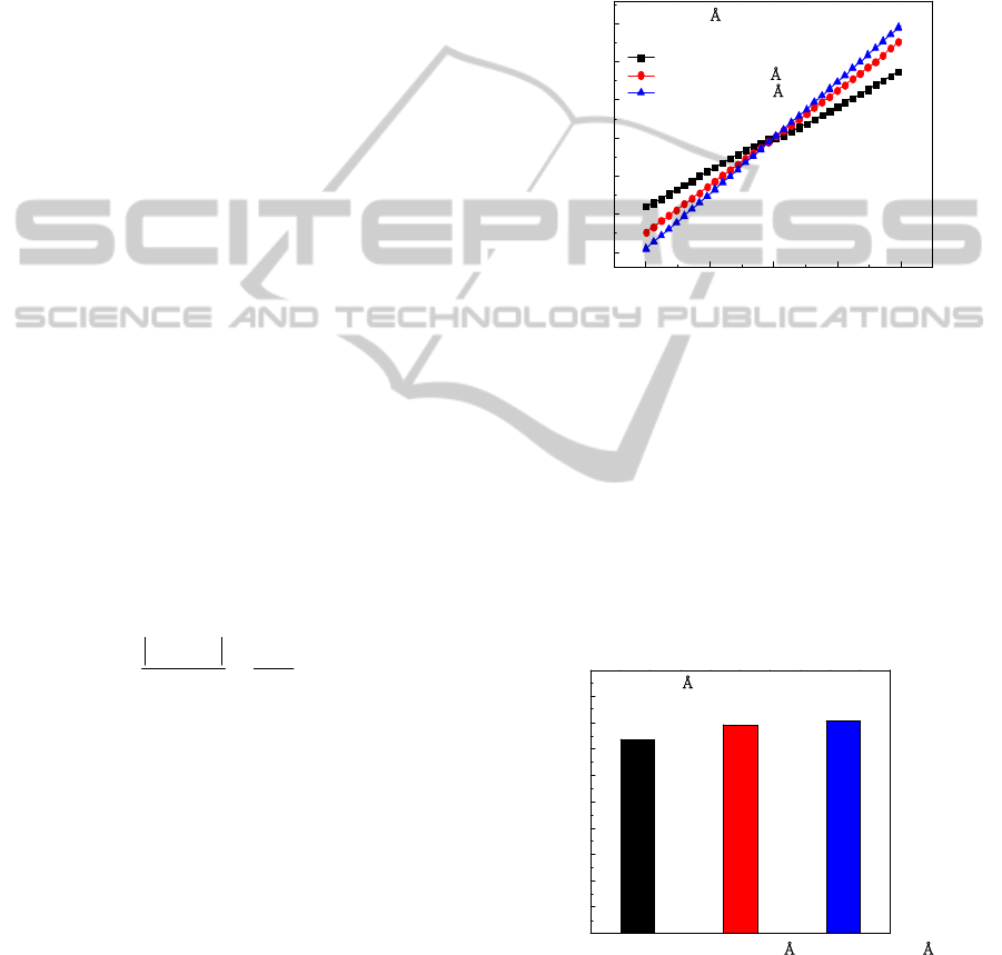
Figure 1 presents the characterization of I-V curve
of the a-Si=200 Å /Si
0.86
Ge
0.14
nanowires with and
without passivation SiO
2
layer. The nanowire with
200 Å passivation layer has higher conductance
compared with the ones with/without 100 Å
passivation layer. The nanowire sensitivity increases
with increasing the nanowire conductance. Figure 2
displays the sensitivity comparison of the nanowires
with/without the passivation oxide layer. Compared
with the nanowire without passivation layer, the
sensitivity increased about 7 and 10 % for 100 and
200 Å passivation layer condition, respectively. By
this way, we found the surface state could be
reduced by this capping layer and oxidation rate also
be reduced. Therefore, the sensitivity can be
improved owing to the lower interface state by
reducing the unstable surface sate and the oxidation
rate.
-10 -5 0 5 10
-1.5x10
-4
-1.0x10
-4
-5.0x10
-5
0.0
5. 0x10
-5
1. 0x10
-4
1. 5x10
-4
Oxidation time : 3min
Current (A)
Voltage ( V)
w/o Pasivation Oxide
Pasivation Oxide=100
Pasivation Oxide= 200
Amorphous 200
Si
0.86
Ge
0.14
Figure 1: The characterization of I-V curve of a-Si=200 Å
/Si
0.86
Ge
0.14
nanowires.
Figure 3 shows the sensitivity of SiGe nanowire
structure with different fraction of Ge. At 20 % Ge
group, the sensitivity has obvious improvement for
the ones with passivation SiO
2
. The sensitivity of 20
% Ge sample was degraded when passivation layer
did not cap on SiGe nanowire. In our previous work,
the sensitivity of SiGe nanowire degraded when the
fraction of Ge exceeded 14%. Therefore the higher
sensitivity of SiGe nanowire with high fraction Ge
was obtained by using a suitable capping layer.
0.0
0.5
1.0
1.5
2.0
2.5
3.0
3.5
4.0
4.5
5.
0
Amorphous 200
Si
0.86
Ge
0. 1 4
oxidation time: 3min
Sen sitivity (% )
w/o Passi vation Passivation Oxide= 10
0
Passivation Oxide= 20
0
Figure 2: The sensitivity comparison of the nanowires
with/without the passivation oxide layer.
Because the oxidation rate was reduced by the
deposition of the SiO
2
layer on the SiGe nanowire,
Ge condensation phenomenon was impacted. Hence,
oxidation time is also another factor to obtain
SURFACE PASSIVATION EFFECT IN SGOI NANOWIRE BIOSENSOR WITH HIGH GE FRACTION
385
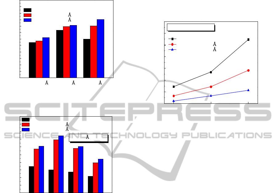
maximum value of sensitivity in passivation
structure.
0.0
0.5
1.0
1.5
2.0
2.5
3.0
3.5
4.0
4.5
5.0
5.5
6.
0
Sensitivity (%)
w/o Passivation Oxide
Passivation Oxide= 100
Passivation Oxide= 200
Oxidaiton time: 3min
a-Si=200
a-Si=200 a-Si=200
Si
0. 9
3
Ge
0.07
Si
0. 8
6
Ge
0.1
4
Si
0.80
Ge
0.20
Figure 3: The sensitivity of SiGe nanowires structure with
different fraction of Ge.
0
1
2
3
4
5
6
7
8
9
1
0
Oxidation Time
a-Si=200 / Si
0. 8
Ge
0.2
3min 5min 7min 10min
w/o Passivation Oxide
Passivation Oxide= 100
Passivation Oxide= 200
Sensitiv ity (% )
Figure 4: The sensitivity of Si
0.8
Ge
0.2
nanowire structure
with different oxidation time.
Figure 4 presents the oxidation time effect in
different passivation conditions of Si
0.8
Ge
0.2
nanowire. The results show that a peak value existed
at the oxidation time of 5 min. The sensitivity was
about 1.3 times greater than the nanowire sample
without the top passivation layer. The sensitivity
degraded while oxidation time increased, resulting
from the poor Ge accumulation at surface when
diffusion effect started to dominated Ge distribution.
Finally, the lower oxidation rate of the sample
with capping layer was verified by the poly-silicon
nanowires. Figure 5 shows the sensitivity of the
poly-silicon nanowires with/without the SiO
2
passivation layer whose oxidation time was split into
three cases (3, 5 and 10 min). The sensitivity of the
poly-silicon nanowire without the SiO
2
passivation
layer was higher than the nanowire with the
passivation layer. This is because of the high
surface-to-volume ratio of poly-silicon without any
passivation layer to reduce oxidation rate. Hence, the
reduction of oxidation rate and unstable surface state
was realized by a suitable capping layer and the
sensitivity of high fraction Ge nanowire can be
improved.
0.6
0.7
0.8
0.9
1.0
1.1
1.2
1.
3
Oxidation Time
Poly silicon nanowire
3min 5min 10min
w/o Passivation Oxide
Passivation Oxide= 100
Passivation Oxide= 200
Sen sitivi ty (%)
Figure 5: The sensitivity of poly-silicon nanowire
structure with different oxidation time.
4 CONCLUSIONS
In our work, a SiO
2
passivation layer is proposed to
reduce the surface state and the oxidation rate for
suppressing the interface formation at the SiGe
surface. Hence, the sensitivity of the sample with a
high fraction Ge can be improved in Ge
condensation process. The maximum improvement
of the sensitivity of the Si
0.8
Ge
0.2
nanowire was
achieved at the oxidation time of 5 min for the
nanowire with 200 Å passivation oxide layer. The
maximum sensitivity enhancement of the passivated
nanowire is around 1.3 times higher than that
without the SiO
2
passivation.
ACKNOWLEDGEMENTS
The authors would like to thank the staff of the
National Nano Device Laboratory for their technical
help. They also acknowledge the financial support of
the National Science Council (NSC) under Contract
Nos. NSC 98-2221-E-009-174-MY3.
REFERENCES
Li, Z., Rajendran, B., Kamins, T. I., 2005. Silicon
nanowires for sequence-specific DNA sensing: device
BIODEVICES 2012 - International Conference on Biomedical Electronics and Devices
386

fabrication and simulation. Applied Physics a-
Materials Science & Processing, 80(6) 1257-1263.
Chang et al., 2011. 4th, 2011 IEEE INEC.
Chang et al., 2008. Higher drive current for SiGe
nanowires. 2
nd
IEEE International Nanoelectronics
Conference, 315-319.
LeGoues, F. K., Rosenberg, R., Nguyen, T., Himpsel, F.,
Meyerson, B. S., 1989. Oxidation studies of SiGe. J.
Appl. Phys, 65(4), 1724.
Tanaka, M., Ohka, T., Sadoh, T., Miyao, M., 2008.
Abnormal oxidation characteristics of SiGe/Si-on-
insulator structures depending on piled-up Ge fraction
at SiO2/SiGe interface. J. Appl. Phys, 103, 054909.
Yang, H., Wang, D., Nakashima, H., Gao, H., Hirayama,
K., Ikeda, K.-i., Hata, S., Nakashima, H., 2008.
Influence of top surface passivation on bottom-
channel hole mobility of ultrathin SiGe- and Ge-on-
insulator. Applied Physics Letters, 93(7), 072104.
SURFACE PASSIVATION EFFECT IN SGOI NANOWIRE BIOSENSOR WITH HIGH GE FRACTION
387
