
High-throughput Hardware Architectures of the JH Round-three
SHA-3 Candidate
An FPGA Design and Implementation Approach
George S. Athanasiou
1
, Chara I. Chalkou
1
, D. Bardis
1
, Harris E. Michail
2
, George Theodoridis
1
and Costas E. Goutis
1
1
Department of Electrical and Computer Engineering, University of Patras, Rio Campus, 26500, Patras, Greece
2
Department of Electrical Engineering and Information Technology, Cyprus University of Technology,
30 Archbishop Kyprianos Str., 3036, Lemesos, Cyprus
Keywords: Security, Cryptography, Hash Functions, SHA-3, JH, High-throughput Implementation, Hardware, FPGA.
Abstract: Hash functions are exploited by many cryptographic primitives that are incorporated in crucial
cryptographic schemes and commercial security protocols. Nowadays, there is an active international
competition, launched by the National Institute of Standards and Technology (NIST), for establishing the
new hash standard, SHA-3. One of the semi-finalists is the JH algorithm. In this paper, two high throughput
hardware architectures of the complete JH algorithm are presented. The difference between them is the
existence of 3 pipeline stages at the second one. They both are designed to support all the possible versions
of the algorithm and are implemented in Xilinx Virtex-4, Virtex-5, and Virtex-6 FPGAs. Based on the
experimental results, the proposed architectures outperform the existing ones in terms of Throughput/Area
factor, regarding all FPGA platforms and JH algorithm’s versions.
1 INTRODUCTION
Authentication is an indispensable feature of almost
all existing cryptographic systems used for securing
e-transactions. The authentication procedure is
accomplished via cryptographic hash functions by
using them as sole authentication modules or
incorporated in hash-based authentication
mechanisms, like the Hashed Message
Authentication Code (HMAC), which is used to
produce Message Authentication Codes (MACs)
(NIST, 2002).
Apart from MAC mechanisms, hashes are used
in many widely-used security applications, such as
IPSec (NIST, 2005b), Public Key Infrastructure
(PKI) (NIST, 2001b), Secure Electronic
Transactions (SET) (Loeb, 1998), etc. Moreover,
digital signature algorithms like DSA that are used
for authenticating services like electronic mail,
electronic funds transfer, electronic data interchange,
data storage etc are based on a critical cryptographic
primitive like hash functions. Furthermore, hashing
cores are also essential for security in networks and
mobile services, as in SSL (Thomas, 2000), which is
a Web protocol for establishing authenticated and
encrypted sessions between servers and clients.
Nowadays, one of the most widely used hash
algorithms, employed in several security
applications and protocols, is SHA-1 (NIST, 2008).
However, in 2005, security issues discovered by
Wang et al. (2005). This attack called into question
the practical security of SHA-1 when used in digital
signatures and other applications requiring collision
resistance. Hence, the adoption of new hash
algorithms, such as SHA-2 family, can be
considered as a secure solution for the future.
Beyond that, to counter the above issues, the
U.S. National Institute of Standards and Technology
(NIST), launched an international competition to
create an entirely new hash algorithm, which will be
called SHA-3 (NIST, 2005a). The competition’s first
round included 51 submissions from which 14
advanced to round two on 2009, where a year was
allocated for a public review. Based on the review’s
feedback, NIST selected the five finalists, which are
promoted to the on-going third (final) round that is
to be finalized at the end of 2012. The third-round
candidates are: BLAKE, Grøstl, JH, Keccak, and
Skein (NIST, 2005a).
126
S. Athanasiou G., I. Chalkou C., Bardis D., E. Michail H., Theodoridis G. and E. Goutis C..
High-throughput Hardware Architectures of the JH Round-three SHA-3 Candidate - An FPGA Design and Implementation Approach.
DOI: 10.5220/0004049801260135
In Proceedings of the International Conference on Security and Cryptography (SECRYPT-2012), pages 126-135
ISBN: 978-989-8565-24-2
Copyright
c
2012 SCITEPRESS (Science and Technology Publications, Lda.)

In this paper, two high-throughput hardware
architectures of the JH algorithm are proposed and
analytically described. The first one incorporates no
pipeline stages while the second one corresponds to
a design with three pipeline stages. Beyond that,
certain design choices were made targeting high
throughput with reasonable area consumption. Both
of them are able to perform as any of the four
versions of JH (JH-224/256/384/512) and were
successfully implemented in Xilinx Virtex-4, Virtex-
5 and Virtex-6 FPGAs. The performance metrics
that are gathered, including Frequency, Area, and
Throughput, show that the proposed architectures
outperform the existing ones in terms of
Throughput/Area cost factor.
The rest of the paper is organized as follows.
Section 2 states the previously published works and
Section 3 presents the JH algorithm, as submitted to
NIST. In Section 4 the proposed architectures are
described in details. The implementation results and
the corresponding comparisons are shown in Section
5, while Section 6 concludes the paper.
2 RELATED WORK
Regarding hardware implementations of the JH
algorithm, to the best of authors’ knowledge, there
are no previously published works dealing with the
JH algorithm itself. However, there are several ones
performing comparative analyses among either the
round-two candidates (Baldwin et al., 2010);
(Henzen et al., 2010); (Tillich et al., 2009); (Matsuo
et al., 2010); (Homsirikamol et al., 2010); (Gaj et al.,
2010); (Guo et al., 2010a); (Guo et al., 2010b);
(Kobayashi et al., 2010), or the round-3 candidates
(Jungk et al., 2011); (Kerckhof et al., 2011); (Guo et
al., 2011); (Guo et al., 2012); (Jungk, 2011);
(Homsirikamol et al., 2011); (Tillich et al., 2010);
(Provelengios et al., 2011). The above studies
include both FPGA and ASIC CMOS
implementations. Specifically, FPGA
implementations and results are reported in 10
papers (Baldwin et al., 2010); (Matsuo et al., 2010);
(Homsirikamol et al., 2010); (Gaj et al., 2010); (Guo
et al., 2010a); (Kobayashi et al., 2010); (Jungk et al.,
2011); (Jungk, 2011); Homsirikamol et al., 2011;
Provelengios et al., 2011).
Apart from (Homsirikamol et al., 2011) and
(Provelengios et al., 2011), all the other works deal
with simple implementations without any form of
optimization. On the other hand, in (Homsirikamol
et al., 2011) pipeline and unrolling investigation
takes place. However it is shown that there are quite
few benefits from both the above techniques.
Regarding (Provelengios et al., 2011), the pipeline
technique is applied, targeting low power desings.
Thus, the reported performance results are low.
Finally, it has to be stressed that, in the
competition’s third round, the JH algorithm is
tweaked (denoted as JH42). The difference between
those two is that the iterations of the first are 36
(plus the potential needed for initialization or
finalization) while the second one’s are 42. This
work deals with JH42 of round-three, which is
considered more efficient for hardware
implementation and offers more security margins
compared to the previous one (Wu, 2008).
3 THE JH ALGORITHM
The hash function family JH, proposed by Hongjun
Wu (2008), includes two main special features: a
new compression structure and a generalized AES
(NIST, 2001a) design methodology. The latter
methodology offers the possibility of easily
constructing large block ciphers from smaller
components. Obviously, the compression structure is
a bijective function implemented as a block cipher
with constant key. The family itself consists of four
versions, namely the JH-224, JH-256, JH-384, and
Jh-512, which are based on the same compression
function but produce a hash value of different width
(via truncation of the output’s bits).
A general diagram of the compression function,
F
d
, is shown in Figure 1. It uses an internal state,
H(i), the size of which is 2
d+2
bits, where the i factor
denotes the i-th iteration and d the dimension of a
block of bits. A d-dimensional block consists of 2
d
4-bit elements. The starting state, H(0), is version-
dependent. In other words, there is a vector, IV,
which is appropriately loaded into the state and
represents the message digest size.
The input message is portioned to n m-bit blocks,
M, through a padding procedure. The compression
operates on a message block, M(n). Initially, the
block is XORed with the lower half of the 2
d+2
-bit
state value. Then, the result is fed in the E
d
function.
The output of E
d
is then XORed once more with the
message block and loaded into the state. If it is the
last block of the message or the message is one-
block then the procedure is over and the hash value
is in the final state. Otherwise, the procedure is
repeated for the next message block.
The E
d
function is based on the d-dimensional
generalized AES methodology and applies
High-throughputHardwareArchitecturesoftheJHRound-threeSHA-3Candidate-AnFPGADesignandImplementation
Approach
127
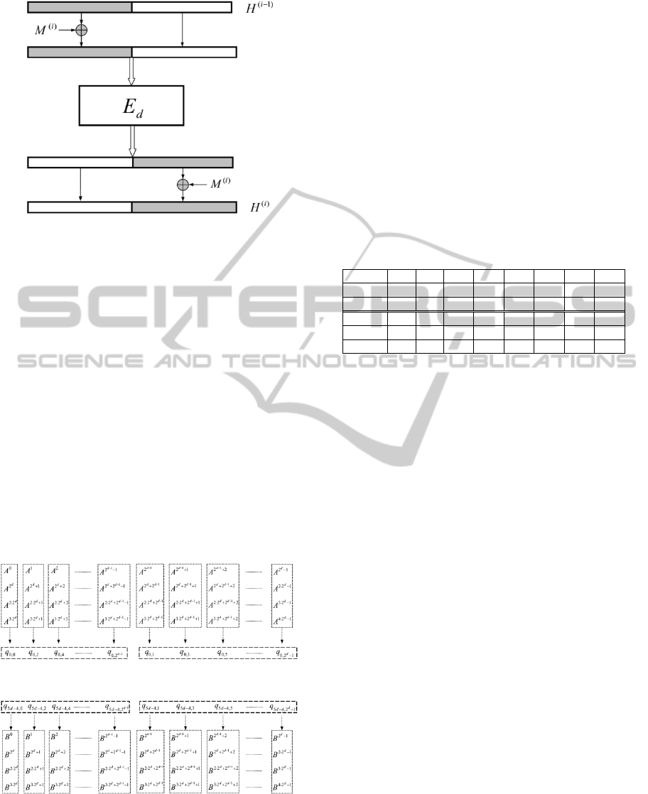
Figure 1: Illustration of the JH compression function F
d
.
Substitution-Permutation Network (SPN) and
Maximum Distance Separable (MDS) codes to a d-
dimensional array. In general, it is mainly
constructed from 6×(d-1) rounds of a round
function, R
d
. Let A and B be the 2
d+2
-bit input and
output of E
d
, respectively. The computation of B =
E
d
(A) is as follows:
1. Grouping the bits of A into 2
d
4-bit elements to
obtain a new quantity, Q
0
.
2. For 6×(d-1) rounds, r, perform Q
r+1
= R
d
(Q
r
,
C
(d)
r
)
3. De-Grouping the 2
d
4-bit elements of Q
6(d-1)
to
obtain B.
Each Q
r
denotes a 2
d+2
-bit word and is equal to (q
r,0
||
q
r,1
|| ... || q
r,2
d
-1
), where each q
r,i
denotes a 4-bit word.
The Grouping procedure is shown in Figure 2
and the De-Grouping procedure in Figure 3,
respectively.
Figure 2: Grouping in E
d
.
Figure 3: De-Grouping in E
d
.
The C
(d)
r
is the 2
d
-bit round constant. These
values are produced by a round function, R
d-2
,
similar to R
d
where all constants being set as zeros.
Each C
(d)
r
is a 2
b
-bit word and is generated as shown
in the following equation:
C
(d)
0
= int[(sqrt(2)-1) × 2^2
d
]
C
(d)
r
= R
d-2
(C
(d)
r
-1
) for r = 1 to 6×(d-1)
(1)
The R
d
function consists of three consecutive layers:
the SBox layer (S), the Linear Transformation layer
(L) and the Permutation Layer (P
d
).
The SBox layer incorporates two types of 4 × 4-
bit S-boxes, namely the S
0
and S
1
. Instead of being
simply XORed to the input, every round constant bit
selects which S-boxes to be used so as to increase
the overall algebraic complexity and thus security.
The S
0
and S
1
S-boxes are shown below:
Table 1: S
0
and S
1
S-boxes.
x 0 1 2 3 4 5 6 7
S
0
(x)
9 0 4 11 13 12 3 15
S
1
(x)
3 12 6 13 5 7 1 9
x 8 9 10 11 12 13 14 15
S
0
(x)
1 10 2 6 7 5 8 14
S
1
(x)
15 2 0 4 11 10 14 8
The Linear Transformation, L, implements a (4,
2, 3) MDS code over GF(2
4
). The multiplication in
GF(2
4
) is defined as the multiplication of binary
polynomials modulo the irreducible polynomial
x
4
+x+1. Hence, letting U, W, Y, and Z four 4-bit
words, the computation of L is showed in Eq. 2.
(Y, Z) = L(U, W) = (5×U + 2×W, 2×U + W) (2)
Finally, the Permutation layer, P
d
, is similar to the
row rotations of AES and is constructed from three
individual permutation functions, π
d
, P’
d
, and φ
d
. All
these functions operate on 2
d
quantities. Letting C, D
are the 2
d
-bit input and output respectively, so as C =
(c
0
, c
1
, ..., c
2d-1
) and D = (d
0
, d
1
, ..., d
2d-1
), the π
d
, P’
d
,
and φ
d
are described by equations 3, 4 and 5
respectively.
d
4i+0
= c
4i+0
, for i = 0 to 2
d-2
– 1
d
4i+1
= c
4i+1
, for i = 0 to 2
d-2
– 1
d
4i+2
= c
4i+2
, for i = 0 to 2
d-2
– 1
d
4i+3
= c
4i+3
, for i = 0 to 2
d-2
– 1
(3)
d
i
= c
2i
, for i = 0 to 2
d-1
– 1
d
i+2d-1
= c
2i+1
, for i = 0 to 2
d-1
– 1
(4)
d
i
= c
i
, for i = 0 to 2
d-1
– 1
d
2i+0
= c
2i+1
, for i = 2
d-2
to 2
d-1
– 1
d
2i+1
= c
2i+0
, for i = 2
d-2
to 2
d-1
– 1
(5)
The P
d
is computed as: P
d
= φ
d
○ P’
d
○ π
d
and is
shown in the following figure (Figure 4).
For the considered JH algorithm, d=8. For more
details about the JH algorithm, the reader is referred
to the submission’s documentation (Wu, 2008).
SECRYPT2012-InternationalConferenceonSecurityandCryptography
128
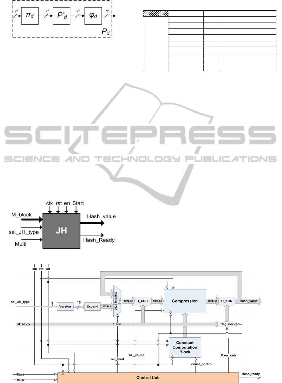
Figure 4: The P
d
permutation.
4 PROPOSED ARCHITECTURES
In this section the two proposed architectures are
presented and analytically described. In more
details, the non-pipelined architecture is described in
Sub-section 4.1, while the three-stage one in Sub-
section 4.2. For clarity reasons, the common parts
between them will be presented once.
4.1 Non-pipelined Architecture
The first architecture that was designed was the non-
pipelined (Figure 5). It includes 7 inputs and two
outputs (Table 2). The output hash value is
dependent to the selected version of the JH.
A block diagram of the above architecture is
presented in Figure 6. It consists of the Data-path
and the Control Unit.
Figure 5: The I/O of the non-pipelined JH module.
Table 2: Input and Output signals of JH architecture.
Name Bits Description
Inputs
clk 1 Clock
rst 1 Reset
en 1 Enable
Start 1 Start computation
M_block 512 Input Block
sel_JH_type 2 JH version selection
Multi 1 One/more blocks
Outputs
Hash_value Ver. Message Digest
Hash_Ready 1 Hash value computed
4.1.1 Data-path
The Data-path includes 7 sub-blocks and a register
that holds the input message block for feeding the
second XOR.
The Version sub-block has as input the
sel_JH_type signal. Based on this, it produces the
appropriate 16-bit signal to be expanded to 1024
bits. This expansion is Expand sub-block’s
responsibility and is accomplished through
concatenation with zeros. The Version sub-block’s
topology is shown in Figure 7.
Right after Expand sub-block there is a 1024-bit
multiplexer which feeds the main computation sub-
blocks with the appropriate data. Actually, this
multiplexer is responsible for the feed-back of the
hash value when it is needed (multiple blocks).
The main computation sub-blocks are the two
XORs and the Compression ones. The XORs are
composed by simple XOR gates and are performing
as indicated in Section 3. The Compression sub-
block is the computation’s core. It performs the JH
compression and, in general, is designed as
described in Section 3. It consists of 6 computation
modules and a 1024-bit register for
Figure 6: Non-pipelined architecture of the JH algorithm.
High-throughputHardwareArchitecturesoftheJHRound-threeSHA-3Candidate-AnFPGADesignandImplementation
Approach
129
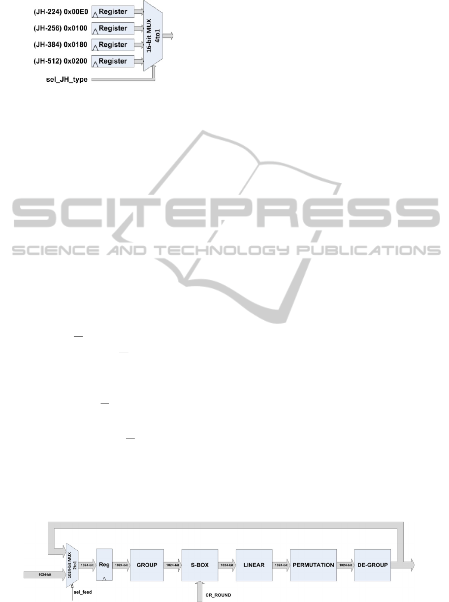
Figure 7: The version sub-block.
synchronization of the iterations (Figure 8).
The main difference of the Compression’s design
compared to the algorithmic description in the
previous section is that the Grouping and De-
Grouping modules are included in the iteration. This
design choice is made in order for the
Compression’s design to be more robust and impose
less routing delay when mapped on the FPGA. The
internal topology of the above two modules are no
complex and designed as described in algorithm’s
section (Section 3). The 1024-bit 2to1 multiplexer is
used for implementing the feed-back of the output,
so as to achieve the iterative process.
The S-BOX module incorporates both S
0
and S
1
S-boxes and its implementation is described in the
computation steps of equation 6. There, x
i
(i = 0 to
3) denotes a 128-bit word, c denotes a 128-bit
constant, t a 128-bit temporal word, while
⊕
&, and
denote XOR, AND, and NOT gates, respectively.
()
()
()
()
()
()
()
()
()
33
00 2
01
00 2 3
33 1 2
11 0 2
22 0 3
00 13
33 1 2
11 0
22
.
. &
. &
. &
. &
. &
. &
. |
. &
. &
.
ix x
ii x x c x
iii t c x x
iv x x x x
vx x x x
vi x x x x
vii x x x x
viii x x x x
ix x x x x
xx x t x
xi x x t
=
=⊕
=⊕
=⊕
=⊕
=⊕
=⊕
=⊕
=⊕
=⊕
=⊕
(6)
The LINEAR sub-block consists of simple XOR
gates. Letting a
i
, b
i
(i = 0 to 7) denote 128-bit words,
the topology is described by equation 7.
005
116
2274
334
441
55 2
66 3 0
77 0
bab
bab
babb
bab
ba a
ba a
ba a a
ba a
=
⊕
=⊕
=⊕⊕
=⊕
=⊕
=⊕
=
⊕⊕
=⊕
(7)
The SBOX and LINEAR modules, due to the fact that
consist of simple logic functions, were designed
together (combined as one hardware module) using
simple logic gates and targeting minimum delay
with balanced area after the mapping on the FPGAs.
Finally, the PERMUTATION module is designed
as simple wire re-arrangement. Thus, it imposes zero
delay. Each of the three individual permutation
functions, π
d
, P’
d
, and φ
d
, for d=4, is shown in
Figures 9, 10, and 11, respectively, considering that
the A, B are 2
d
-bit words, so as A = (a
0
, a
1
, ..., a
2d-1
)
and b = (b
0
, b
1
, ..., b
2d-1
).
Combining those three, the wire re-arrangement
for P
d
permutation (d = 4), is given by Figure 12.
The data input CR_ROUND is coming from the
Constant Computation Block. This block computes
the appropriate constant values for each round.
This computation is chosen to be done in parallel
with the Compression computation (on-the-fly). This
way, extra registers and control logic for storing and
steering the constant values is avoided. Internally,
the Constant Computation Block is similar to the
Compression module. However, its data width is 256
bits, as imposed by the algorithm.
4.1.2 Control Unit
The control of the architecture is accomplished by
the Control Unit. This unit implements a non-
complex Finite State Machine (FSM) with 5 states,
namely the Idle, Initiate, Compress,
Figure 8: Compression sub-block.
SECRYPT2012-InternationalConferenceonSecurityandCryptography
130
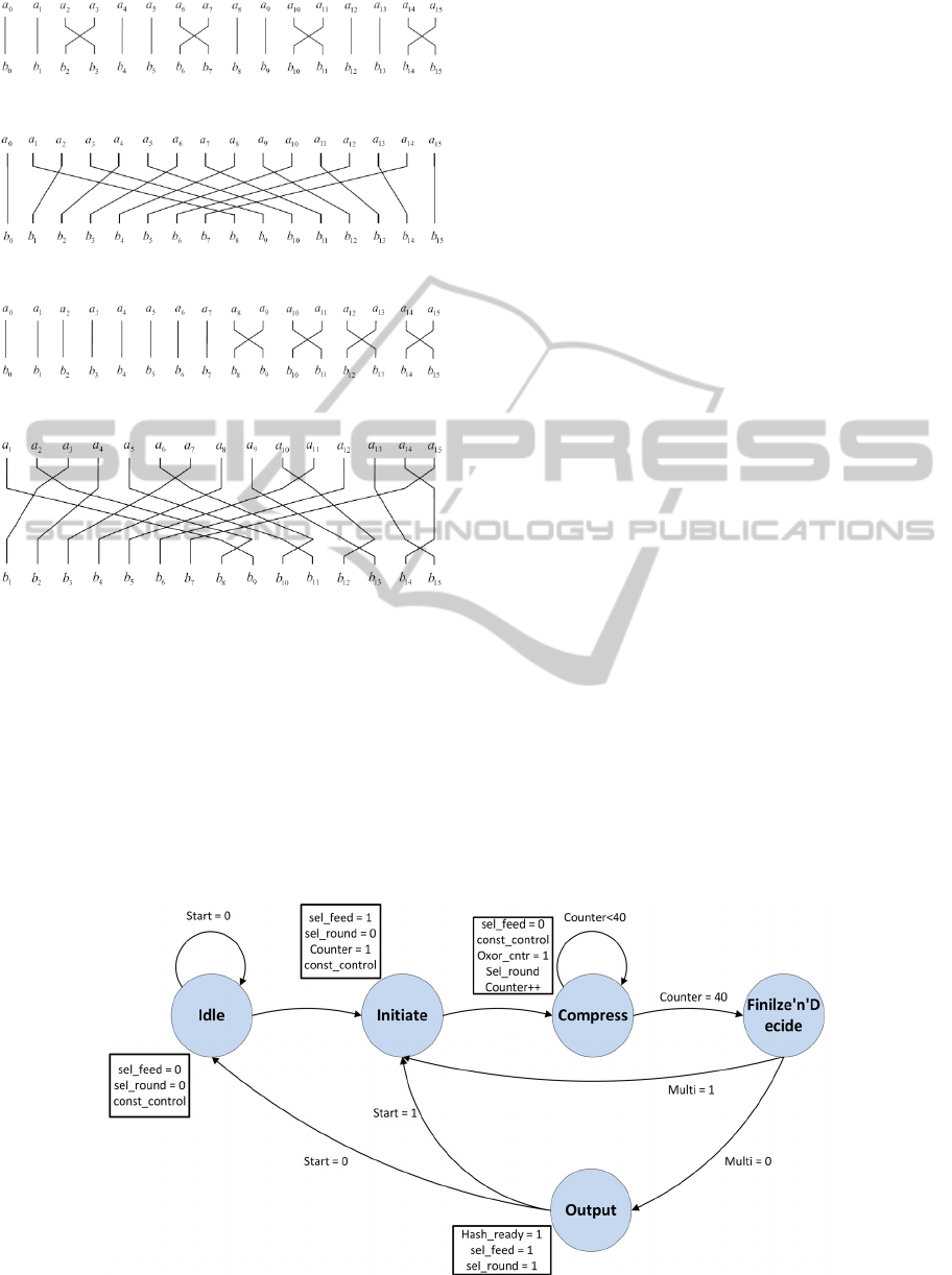
Figure 9: The π
4
permutation.
Figure 10: The P’
4
permutation.
Figure 11: The φ
4
permutation.
Figure 12: The P
4
permutation.
Finilze’n’Decide, and, Output (Figure 13). Its design
consists of a counter that counts up to 42, registers,
and simple logic gates.
Initially, the system is in the Idle state and if
there is a message block for processing (Start=1)
moves to Initiate state where the system remains for
one clock cycle. There the selection of the type, the
expansion, and the first XORing take place, along
with the first iteration of the compression. Then, the
system moves to state Compress, where 40 of the
iterations are accomplished (40 cycles). At the
fortieth iteration the systems moves to
Finilize’n’Decide state where the last iteration (42
nd
)
takes place along with the last XORing. There, if
there is another block of the same message (Multi =
1), then the computation starts again for the second
block and the system flips to Initiate. If not (last or
one-block message), then the final state of the
system is the Output where the hash_value is popped
out and the Hash_ready signal is set to 1.
The system’s full operation is 42 + 1 (output’s
steering) = 43 cycles for a 512-bit input message
block. In Figure 13, inside the text boxes next to the
states there are the values of some significant control
signals. These values are active during the very next
clock cycle, after their assignment.
4.2 Three-stage Pipelined Architecture
The second proposed architecture, which is
concerned as one of the main contributions of this
work, is the three-stage pipelined. To achieve the
pipeline, two stages of internal (pipeline) registers
are inserted in the architecture of Figure 6,
portioning the compression procedure into three
separate stages, named Compression 14. Each one of
these blocks iterates 14 times (3 × 14 = 42 in total).
To feed the above blocks with the appropriate
constant values, two additional Constant
Computation blocks were added, separated by
registers (Pipe Regs). Beyond that, the 512-bit input
block’s bus is fed into two additional, consecutive,
registers in order to be correctly synchronized with
the rest computation.
The internal functionality of both the
Compression 14 and the Constant Computation
Figure 13: State diagram of the control unit’s FSM of the non-pipelined architecture.
High-throughputHardwareArchitecturesoftheJHRound-threeSHA-3Candidate-AnFPGADesignandImplementation
Approach
131
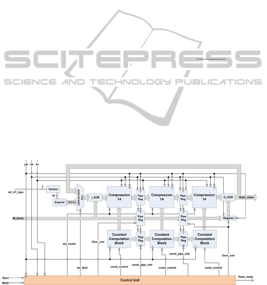
blocks are identical with the ones of the Non-
Pipelined architecture. The same goes for the
Version and Expand blocks. The data width is the
same as the non-pipelined architecture.
Concerning the control of this architecture, the
designed Control Unit consists of the same states as
before (Figure 13). However, it is larger and
produces more control signals. Specifically, it
includes more combinational logic and three
counters, one for every Compression 14 block, that
count up to 14. Each one of them is activated and
performs during the computation of the
corresponding Compression 14 block. Additionally,
they produce the sel_round, const_pipe_cntr and
const_control control signals. Beyond the above
counters, there is one more that is activated only
when the current input block is followed by another
block of the same message. This counter counts up
to three and, in combination with the Multi input
signal, produces the sel_feed control signal.
5 IMPLEMENTATION RESULTS
AND COMPARISONS
The proposed architectures of JH hash algorithm
were captured in VHDL hardware description
language, synthesized, and implemented in FPGA
technology using the XST synthesize tool of the
Xilinx ISE Design Suite, v.13.1. The correct
functionality of the proposed JH cores was, initially,
verified through Post-Place and Route (Post-P&R)
simulation via the Model Technology’s ModelSim
simulator. A large set of test vectors, apart from the
official known-answer tests (KATs), were used.
Thereafter, downloading to actual FPGA boards
was performed. Three widely known FPGA families
were selected to implement the introduced design,
namely the Xilinx Virtex-4 (xc4vlx160-FF1148, -
12), Virtex-5 (xc5vfx130t-FF1738, -3), and Virtex-6
(xc6vlx365t-FF1759, -3). The implementations’
correct functionality was verified once again on the
board via Xilinx ChipScope tool.
The considered implementation metrics were:
Frequency (MHz), Occupied Area (Slices) and
Throughput (Mbps). The Throughput metric of our
designs, similarly to the existing studies dealing with
hardware implementations of the JH, is given by the
following equation:
(
)
# bits F
Throughput
C
×
=
(8)
where F and C refer to the frequency and clock
cycles of the JH operation, while the #bits denotes
the number of data bits that are processed by the
algorithm during C cycles. In the following tables
the above mentioned performance metrics for the
proposed Non-Pipelined (Pro. NP) and Three-Stage
Pipelined (Prop. 3P) architectures, along with the
corresponding comparisons, are presented per FPGA
family. The * and ** next to a reference denote that
this metrics concern JH-256 and JH-512,
respectively. The other works do not specify the
version or the metrics are common for all of them.
Figure 14: Three-stage pipelined architecture of the JH algorithm.
SECRYPT2012-InternationalConferenceonSecurityandCryptography
132
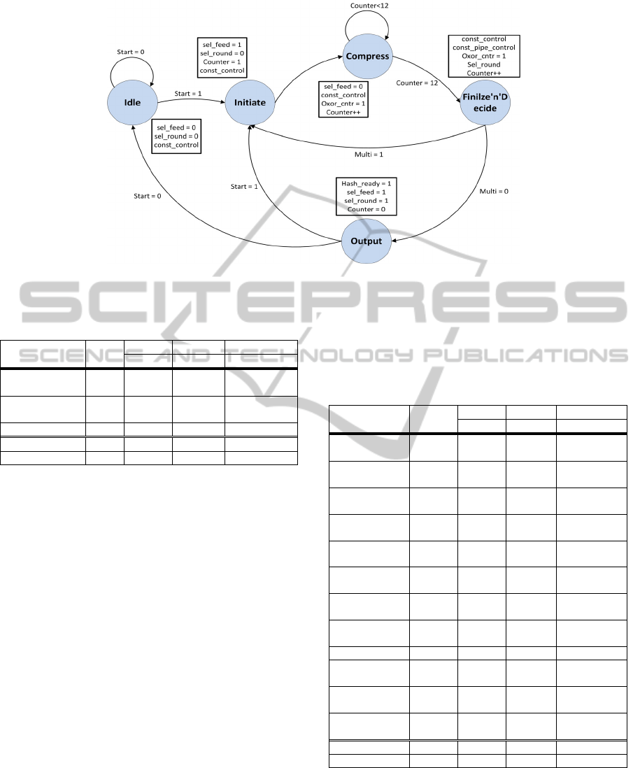
Figure 15: State diagram of the control unit’s FSM of the three-stage pipelined architecture.
Table 3: Implementation results and comparisons for
Xilinx Virtex-4 technology.
Ref. C.R.
Freq. Area Throughput
(MHz) (Slices) (Mbps)
Homsirikamol
et al., 2010)*
R2 276.93 3,737 3,942.2
Homsirikamol
et al., 2010)**
R2 256.64 3,787 3,650
Gaj et al., 2010 R2 194.18 4,122 2,761.6
Prop. NP R3 328.3 3,143 3,909.1
Prop. 3P R3 339.8 8,529 11,598.5
The comparisons show that the proposed
architectures are more efficient in terms of
Throughput, compared to almost all existing works.
Specifically, there is only one study (Homsirikamol
et al., 2010) that presents better Throughput results,
than those of the proposed Non-Pipelined (NP)
architecture. However, this work (along with others
indicated in the above tables) considers the JH
algorithm’s version of the Second Round of the
SHA-3 competition (Competition Round’s
Specifications – C.R. = Round 2 – R2). Our work, on
the other hand deals with the JH algorithm’s version
of the Third Round (C.R. = R3). The latter version
includes a few tweaks compared to the one of the
Second Round the most crucial of which is the
number of the algorithm’s iterations. In more details,
Second Round’s version iterates 35.5 times contrary
to the Third Round’s one that iterates 42. This
number plays a key role to the computation of the
Throughput metric because it is used as the
denominator of the Throughput fraction of equation
7. For example, this is the reason why the
Throughput results of Homsirikamol et al. (2010)
are better, compared to the ones of this work, even
though our achieved Frequency is higher and the
#bits value is equal to 512 for both studies. Overall,
the direct comparison among works of different
round specifications is not completely fair.
Table 4: Implementation results and comparisons for
Xilinx Virtex-5 technology.
Ref. C.R.
Freq. Area Throughput
(MHz) (Slices) (Mbps)
Baldwin et
al., 2010
R2 220.13 1,291 1,941
Matsuo et al.,
2010
R2 201 2,661 2,639
Homsirikamol
et al., 2010)*
R2 380.8 1,018 5,416
Homsirikamol
et al., 2010**
R2 394.48 1,104 5,610.4
Gaj et al.,
2010
R2 213.77 1,569 3,040.2
Guo et al.,
2010a
R2 182.6 2,406 2,597
Kobayashi et
al., 2010
R2 201 2,661 2,639
Jungk et al.,
2011
R3 283 193 23
Jungk, 2011 R3 271 555 237
Homsirikamol
et al., 2011*
R3 - 917 4,725
Homsirikamol
et al., 2011**
R3 - 914 4,725
Provelengios
et al., 2011
R3 201.2 2,251 1,328
Prop. NP R3 434.8 922 5,176.9
Prop. 3P R3 439.2 2,496 14,991.4
Beyond the above, a fairer comparison and
evaluation factor, namely the Throughput/Area, is
included. In the following three figures, the
comparison in terms of the above factor, between the
proposed architectures and the previously published
ones, is illustrated.
High-throughputHardwareArchitecturesoftheJHRound-threeSHA-3Candidate-AnFPGADesignandImplementation
Approach
133
As it can be seen, the proposed NP architecture is
the most efficient in terms of Throughput/Area
among the other existing works, even from the ones
implementing the JH version of Competition’s
Second Round. Regarding the Three-stage Pipelined
(3P) the improvements are greater.
Table 5: Implementation results and comparisons for
Xilinx Virtex-6 technology.
Ref. C.R.
Freq. Area Throughput
(MHz) (Slices) (Mbps)
Homsirikamol
et al., 2010)*
R2 415.46 959 5,903.4
Homsirikamol
et al., 2010)**
R2 412.54 1,076 5,867.2
Kerckhof et
al., 2010
R3 299 304 222
Prop. NP R3 457.3 881 5,445.1
Prop. 3P R3 461.7 2,483 15,759.4
Figure 16: Throughput/area comparisons for Virtex-4
FPGA technology.
Figure 17: Throughput/area comparisons for Virtex-5
FPGA technology.
Figure 18: Throughput/area comparisons for Virtex-6
FPGA technology.
6 CONCLUSIONS
In this paper, two high-throughput designs for JH
SHA-3 candidate were presented. The difference
between them is that the second one included three
stages of pipeline, increasing its performance.
Implementation and measurements were performed
in FPGA boards that showed that the proposed
designs outperform in terms of Througput/Area
compared to other FPGA implementations of JH
algorithm, previously published by academia.
REFERENCES
Baldwin, B., Byrne, A., Hamilton, M., Hanley, N.,
O’Neill, M., Marnane, W.P., 2010. FPGA
Implementations of the Round Two SHA-3
Candidates. In International Conference on Field
Programmable Logic and Applications (FPL).
Gaj, K., Homsirikamol, E., Rogawski, M., 2010.
Comprehensive comparison of hardware performance
of fourteen round 2 SHA-3 candidates with 512-bit
outputs using field programmable gate arrays. In
Second SHA-3 Conference.
Guo, Xu, Huang, Sinan, Nazhandali, Leyla, Schaumont,
Patrick, 2010a. On the Impact of Target Technology in
SHA-3 Harware Benchmark Rankings. Cryptology
ePrint, Archive, Report 2010/536.
Guo, Xu, Sinan H., Nazhandali, L., Schaumont, P., 2010b.
Fair and Comprehensive Performance Evaluation of
14 Second Round SHA-3 ASIC Implementations. In
The Second SHA-3 Candidate Conference.
Guo, Xu, Srivistav, Meeta, Huang, Sinan, Ganta, Dinesh,
Henry, B., Michel, Nazhandali, Leyla, Scaumont,
Patrick, 2011. Silicon Implementation of SHA-3
Finalists: BLAKE, Grostl, JH, Keccak and Skein. In
Workshop on ECRYPT II Hash.
Guo, Xu, Srivistav, Meeta, Huang, Sinan, Ganta, Dinesh,
Henry, B., Michael, Nazhandali, Leyla, Schaumont,
Patrick, 2012. ASIC Implementations of Five SHA-3
Finalists. In Europe Conference Exhibition on Design,
Automation Test.
Henzen, L., Gendotti, P., Guillet, P., Pargaetzi, E., Zoller,
M., Gurkaynak, K., F., 2010. Developing a Hardware
Evaluation Method for SHA-3 Candidates.
Cryptographic Hardware and Embedded Systems,
Springer Berlin / Heidelberg, pp. 248-263.
Homsirikamol, E., Rogawski, M., Gaj, K., 2010.
Comparing Hardware Performance of Fourteen Round
Two SHA-3 Candidates Using FPGAs. Cryptographic
Hardware and Embedded Systems, Springer Berlin /
Heidelberg, pp. 264-278.
Homsirikamol, E., Rogawski, M., Gaj, K., 2011.
Comparing hardware performance of round 3 SHA-3
candidates using multiple hardware architecture in
Xilinx and Altera FPGAs. In Workshop on ECRYPT II
Hash.
SECRYPT2012-InternationalConferenceonSecurityandCryptography
134

Jungk, B., 2011. Compact Implementations of Grostl, JH
and Skein for FPGAs. In Workshop on ECRYPT II
Hash.
Jungk, B., Apfelbeck, J., 2011. Area-efficient FPGA
Implementations of the SHA-3 Finalists. In
International Conference on Reconfigurable
Computing and FPGAs (ReConFig), pp.235-241,
Hochschule RheinMain, Wiesbaden, Germany.
Kerckhof, Stéphanie, Durvaux, François, Veyrat-
Charvillon, Nicolas, Regazzoni, Francesco, 2011.
Compact FPGA implementations of the five SHA-3
finalists. In Workshop on ECRYPT II Hash.
Kobayashi, K., Ikegami, J., Knezevic, M., Guo, E., X.,
Matsuo, S., Huang, S., Nazhandali, L., Kocabas, U.,
Junfeng Fan Satoh, A., Verbauwhede, I., Sakiyama,
K., Ohta, K., 2010. Prototyping platform for
performance evaluation of SHA-3 candidates. In
International Symposium on Hardware-Oriented
Security and Trust (HOST), IEEE, pp.60-63.
Loeb, L., 1998. Secure Electronic Transactions:
Introduction and Technical Reference. Artech House
Publishers. Norwood, USA.
Matsuo, S., Knezevic, M., Schaumont, P., Verbauwhede,
I., Satoh, A., Sakiyama, K., Ohta, K., 2010. How Can
We Conduct ‘‘Fair and Consistent’’ Hardware
Evaluation for SHA-3 Candidate? In 2nd SHA-3
Conference.
NIST, 2001a. Advnaced Encryption Standard. FIPS-197,
NIST, Department of Commerce Publications, USA.
NIST, 2001b. Introduction to Public Key Technology and
the Federal PKI Infrastructure. SP 800-32., NIST, US
Department of Commerce Publications, USA.
NIST, 2002. The Keyed-Hash message authentication
code (HMAC). NIST-FIPS 198, NIST, US Department
of Commerce Publications, USA.
NIST, 2005a. SHA-3 Cryptographic Hash Algorithm
Competition. [online] Available at: http://csrc.nist.gov/
groups/ST/hash/sha-3/index.html [Accessed on:
March, 9 2012]
NIST, 2005b. Guide to IPSec VPN’s. NIST-SP800-77,
NIST, Department of Commerce Publications, USA.
NIST, 2008. Secure Hash Standard (SHS). NIST-FIPS
180-3, Department of Commerce Publications, USA.
Provelengios, G, Voros, S., N., Kitsos, P., 2011. Low
Power FPGA Implementations of JH and Fugue Hash
Functions. In 14th Euromicro Conference on Digital
System Design (DSD), pp.417-421.
Thomas, S., 2000. SSL & TLS Essentials: Securing the
Web, John Wiley and sons Publications. New York,
USA.
Tillich, S., Feldhofer, M., Kirschbaum, M., Plos, T.,
Schmidt, J.-M., Szekely, A., 2009. High-Speed
Hardware Implementations of BLAKE, Blue Midnight
Wish, CubeHash, ECHO, Fugue, Grostl, Hamsi, JH,
Keccak, Luffa, Shabal, SHAvite-3, SIMD, and Skein.
Cryptology ePrint, Archive, Report 2009/510.
Tillich, S., Feldhofer, M., Kirschbaum, M., Plos, T.,
Schmidt, J.-M., Szekely, A., 2010. Uniform evaluation
of hardware implementations of the round-two SHA-3
candidates. In Second SHA-3 Conference.
Wang, X., Yin, Y., L., Yu, H., 2005. Finding collisions in
the full SHA1. In Proceedings of Crypto on Springer
Lecture Notes in Computer Science (LNCS), vol.3621
pp.17-36.
Wu, Hongjun, 2008. The hash function JH. National
Institute of Standards and Technology (NIST).
High-throughputHardwareArchitecturesoftheJHRound-threeSHA-3Candidate-AnFPGADesignandImplementation
Approach
135
