Simulation of the Thermal Management of the Semiconductor
Disk Laser
Yanrong Song, ZhenHua Yu, Peng Zhang and Zili Li
College of Applied Sciences, Beijing University of Technology, Beijing 100124, China
Keywords: Optically Pumped Semiconductor Disk Lasers, Finite-Element Analysis Method, Thermal Management.
Abstract: For the optically pumped semiconductor disk lasers, the thermal problem is the key to obtain the high out
power. To solve this problem, we simulated the heat distribution of the gain chip by finite-element analysis
method to discover the heat spread affected by the thickness of the substrate and found the outstanding heat
spread result of the diamond chip.
1 INTRODUCTION
The semiconductor disk laser (SDL), which is also
known as the Vertical external cavity surface
emitting laser (VECSEL) (Kuznetsov, 1999),
combining the advantages of compact, small size,
low loss and good beam quality (Maclean, 2008), is
an ideal candidate for applications such as
biomedicine (Daukantas, 2007), high density optical
data storage (Risk, 2003), chemical sensor
(Garnache, 2005), and pump sources for other lasers
(Richter, 2005).
In the past decade, output powers of SDL s
have been upgraded significantly, but still not very
high. Limitations to the output power of a V SDL
come from the heat effects. With the deposited heat,
thus increased temperature, the gain of quantum
wells (QWs) will decrease sharply, and the laser
wavelength will redshift so the periodic resonant
gain structure will be detuned (Corzine,1989).What
is more, the nonradiative recombination will become
dominant and the temperature rise will be further
accelerated. All of the above factors are
compounded until finally the thermal rollover of the
laser occurs.
Numerical analysis can give an overall pattern
of the generation, deposition and dissipation of heat
in a SDLs, and therefore bring forward advanced
thermal management to improve the thermal
properties and upgrade the output power of the laser.
A finite element analysis was used by Kemp et al. to
study the heatspreader approach; the required
properties of a heatspreader were examined and the
effect on heat flow and thermal lens effects were
discussed.
Here we present a numerical analysis of
thermal effect in InGaAs system SDL. We
discovered the heat spread affected by the thickness
of the substrate and found the outstanding heat
spread result of the diamond chip.
2 NUMERICAL METHODS
2.1 Model for Thermal Simulation
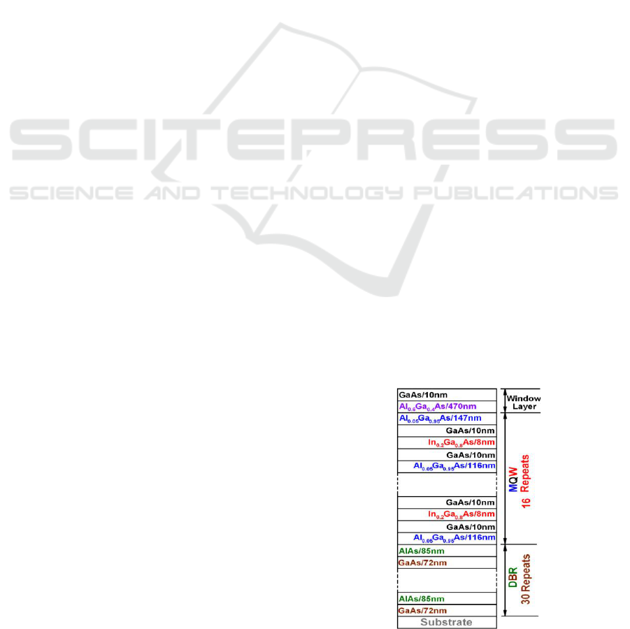
Figure 1: The epitaxial structure of the simulated
semiconductor wafer.
The epitaxial structure of the simulated
semiconductor wafer is shown in Fig. 1. We divide
231
Song Y., Yu Z., Zhang P. and Li Z..
Simulation of the Thermal Management of the Semiconductor Disk Laser.
DOI: 10.5220/0004056902310233
In Proceedings of the 2nd International Conference on Simulation and Modeling Methodologies, Technologies and Applications (SIMULTECH-2012),
pages 231-233
ISBN: 978-989-8565-20-4
Copyright
c
2012 SCITEPRESS (Science and Technology Publications, Lda.)
the whole structure into four parts: the window
layer, the multiple QWs, the DBR and the substrate.
The total thermal conductivity in axial and radial
direction of each part including multiple layers can
be written as
i
ii
t
tk
k
(1)
And the total absorption coefficient of each
part is obtained by
i
ii
t
t
(2)
where
i
k
and
i
are the thermal conductivity
and absorption coefficient of the ith layer, and
i
t
is
the thickness. In the computation, the wavelengths
of pump and laser are 808 and 1040 nm; the value of
0.475µm
-1
for the absorption coefficient of GaAs
layer and 1µm
-1
for the absorption coefficient of
In0.2Ga0.8As/Al0.05Ga0.95As QWs are used.
Then, the temperature, the heat flux and the
gradient of temperature can be obtained by solving
the standard heat equation (steady state):
QTk
(3)
where k is the thermal conductivity and T is the
temperature.
The heat loading density Q is calculated by
www
ww
w
zz
r
P
Q
0
2
2
2
exp
2
exp
2
(4)
where
w
is the fraction of absorbed pump
power that goes to heating, andη=1-λ
pump
/λ
laser
in
MQWs part and η=1 in other parts. α is the
absorption coefficient of each part, r is the
coordinate in radial direction and z is the coordinate
in axial direction. The start position z0 of each part is
different and the start position of window layer is
chosen to be zero. In this paper, the pump power and
the pump spot radius are assumed to be 10W and 50
mm unless there is a special explanation.
Table 1: Parameters of some materials.
Material
k (Wm
-1
K
-1
)
α (µm
-1
)
GaAs
44
0.457
AlAs
91
0
Al
0.6
GaAs
11
0
Al
0.05
GaAs
27
1.000
In
0.2
GaAs
7
1.000
Diamond
2000
0
2.2 Results of the Simulation
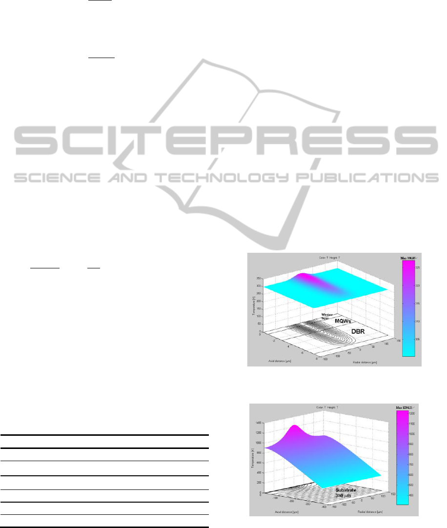
We used the finite-element analysis method to
simulate the heat distribution of the semiconductor
chip when the heat sink temperature was 300 k. The
parameters used is in table 1. We could discovery
the heat spread affected by the thickness of the
substrate illustrated in Fig.2. and Fig.3. We also can
find the outstanding heat spread result of the
diamond chip from Fig.3. and Fig. 4.
The Fig.2 described the temperature variation
when the thickness of the gain chip substrate is 0
µm, the maximum temperature rise is 30.05 K,
compare to the 934.21 K of the max temperature rise
represented in Fig.3. when the thickness of the gain
chip is 350 µm. So the substrate removal is an
effective method to improve the heat spread of gain
chip.
At the same time, a 300µm-thick diamond chip
was bonded on the gain chip with 350 µm substrate,
as shown in Fig. 4. The maximum temperature rise
is 56.79 K, which is much lower than the 934.21 K
shown in Fig.3. Therefore, the diamond has
outstanding heat spread results. Whilst using
heatspreader has superior heat spread effect, and
we’ll try to bonding the diamond on the gain chip to
obtain higher fundamental power so as to get higher
harmonic power in our next work.
Figure 2: Heat distribution of the semiconductor chip
without substrate.
Figure 3: Heat distribution of the semiconductor chip
when its substrate is 350 µm-thick.
SIMULTECH 2012 - 2nd International Conference on Simulation and Modeling Methodologies, Technologies and
Applications
232
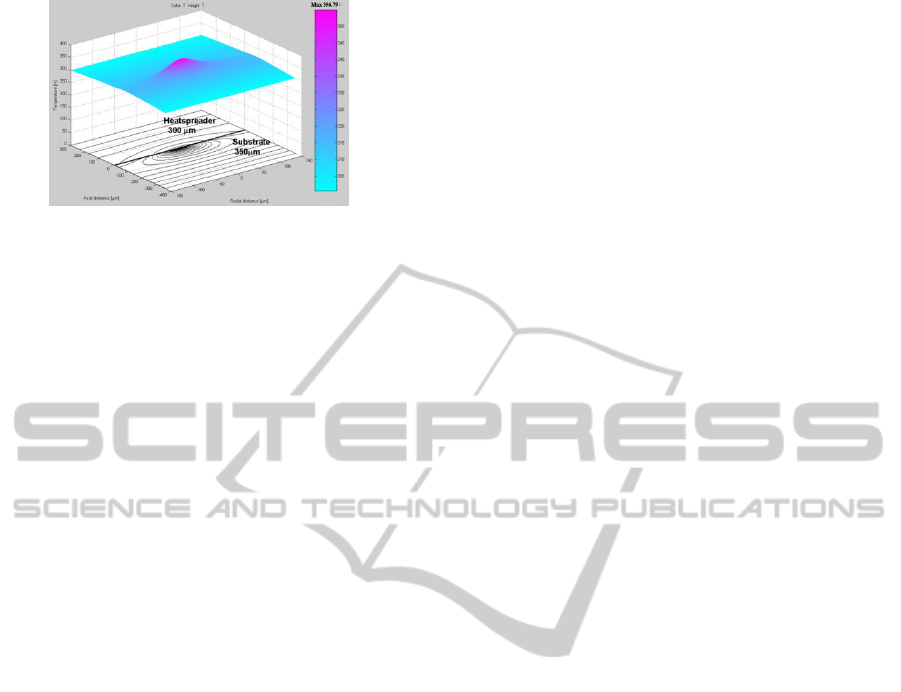
Figure 4: Heat distribution of the semiconductor chip with
its 350 µm-thick substrate which is bonded a 300µm-thick
diamond heatspreader.
3 CONCLUSIONS
In this papser, the thermal distribution has been
discussed and the simulation results has been
demonstrated by finite-element analysis method.
Using the model, we could optimize the SDL and
obtain higher output power.
ACKNOWLEDGEMENTS
This work is supported by the National Natural
Science Foundation of China ( Grant No
61177047).
REFERENCES
M. Kuznetsov. F. Hakimi, R. Sprague, and A. Mooradian,
IEEE J. Sel. Top. Quantum Electron, 5. 516-573, 1999,
“Design and characteristics of high-power (>0.5-
WCW) diode-pumped vertical –external-cavity
surface-emitting semiconductor lasers with circular
TEM00 beams”.
A J. Maclean, Alan J. Kemp, Stephane Calvez, IEEE
44,3,2008, “Continuous Tuning and Efficient
Intracavity Second-Harmonic Generation in a
Semiconducot Disk Laser With an Intracavity
Diamond Heaterspreader”
P. Daukantas, Opt. Photon, News. 18, pp. 20-27,2007
“Optics in forensics: Separating science from fiction”.
W. P. Risk, T. R. Gosnell, and A. V. Nurmikko, 2003,
“Compact blue-green lasers” (Cambridge University
Press, UK)
A. Garnache, A. Liu, L.Cerutti, and A. Campargue, Chem.
Phys. Lett., 416, 22-27, 2005, “Intracavity laser
absorption spectroscopy with a vertical external cavity
surface emitting laser at 2.3µm: Application to water
and carbon dioxide”.
A. Richter, H. Scheife, E. Heumannn, G. Huber, W.
Seelert, and A. Diening, Electron. Lett., 41, 794-795,
2005, “Semiconductor laser pumping of continuous-
wave Pr3+-doped zblan fibre laser”.
S. W. Corzine, R. S. Geels, J. W. Scott, R. H. Yan, and L.
A. Coldren: IEEE J. Quantum Electron. 25,1513. 1989
Simulation of the Thermal Management of the Semiconductor Disk Laser
233
