
All-optical Multi-wavelength Virtual Memory Architecture
Design and Performances Analysis
Selma Batti
1
, Mourad Zghal
2
and Noureddine Boudriga
1
1
Communication Networks and Security Laboratory (CNAS), Engineering School of Communication of Tunis (Sup’Com),
University of Carthage, Ariana, Tunisia
2
CIRTA’COM Laboratory, Engineering School of Communication of Tunis (Sup’Com), University of Carthage,
Ariana, Tunisia
Keywords: Optical Buffering, All-optical Memory, Fiber Bragg Grating, Tunable Wavelength Conversion.
Abstract: As all-optical memory represents one of the most important lacks in evolution of optical networks; this
paper presents an all-optical virtual memory based on a recirculation loop, with the goal of providing optical
data unit storage in all-optical switching networks. The concept of multi-wavelength signal buffering is
adopted, to realize a shared buffer with an important storage capacity. We propose the organization of the
buffer in two loops, the first as a delay loop and the second as an amplification loop, to improve the
buffering duration and performances. The memory implementation is demonstrated using optical
components such as fiber Bragg gratings (FBG), circulator and tunable wavelength converter. An all-optical
control unit is designed to provide a dynamic and automatic signal buffer managing. An analytical model is
implemented and a simulations set is done to prove that the proposed architecture is able to confine several
signals for a relatively long time as a memory and signals can leave the architecture for a reasonably short
delay after the departure decision is taken. The low penalty observed shows good system reliability.
1 INTRODUCTION
To resolve the increasing need of capacity,
networking is interesting more and more in optical
technologies. However, the absence of optical
memory causes a bottleneck due to the optical-
electronic-optical signal conversion. To improve
optical network performances, all-optical memory is
considered as a crucial point. The design of optical
memory has important effect on the development of
all-optical network and more especially on optical
switching node by reducing the impact of some
technical problems such as contention resolution
(Mack et al., 2010).
We define all-optical virtual memory as a device
able to deliver a signal identical to the received one
but after a certain delay. Optical data would be kept
in optical format throughout the storage time without
being converted into electronic format. The multi-
wavelength memory must be able to enclose several
signals having different wavelengths values at the
same time and each one can be delivered
independently of the others. To be considered as
acceptable, optical buffers must minimally provide
some criteria (Burmeister et al., 2008), such as being
bit rate scalable to greater than 40 Gbits/s, being
able to memorize data units having at least 40 bytes
as size additional to their guard bands and providing
dynamically variable memorization time.
A wide variety of architectures has been
proposed in the literature for the design of optical
buffer. Two main techniques were developed: fiber
delay line (FDL) and recirculation loop. The time
buffer described in (LeGrange et al., 2007) is based
on FDL. The architecture is proposed particularly to
be implemented inside an all-optical router. It
utilizes fast wavelength switching in combination
with an arrayed waveguide grating (AWG) to select
a particular FDL from an array of FDL of varying
length. An integrated optical device consisting of the
silicon delay line and the gate matrix operating as a
buffer at 40 Gbits/s is demonstrated in (Park et al.,
2008). Once optical packets are routed into the delay
line, they are stored in the delay line until the gate
matrix switch re-routes them to the output. The gate
matrix switch is controlled by an electronic device.
Offering a particular small size and a low cross talk,
the chosen components enable a 1.1 ns delay of 40
Gbits/s data packets after one turn.
388
Selma Batti S., Zghal M. and Boudriga N..
All-optical Multi-wavelength Virtual Memory Architecture - Design and Performances Analysis.
DOI: 10.5220/0004071403880395
In Proceedings of the International Conference on Data Communication Networking, e-Business and Optical Communication Systems (OPTICS-2012),
pages 388-395
ISBN: 978-989-8565-23-5
Copyright
c
2012 SCITEPRESS (Science and Technology Publications, Lda.)
In this work, we propose an all-optical multi-
wavelength virtual memory (MWVM). Using all-
optical technologies even for the control part, the
virtual memory is designed to confine optical signals
without resort to electrical conversion during the
stay time in the buffer. The multi-wavelength
concept allows the share of the unique buffer
resource by several signals. Organizing the memory
in two loops by isolating the amplifier in a second
loop improves the memory performances through
guarantee adequate power level and avoiding
additional noise amplification. Moreover, we size
the duration of a first loop to reduce the delay
between the moment of the exit decision and the
signal deliverance and to provide an enough long
buffering duration. Work presented in (Batti et al.,
2010) describes an all-optical virtual memory
allowing the confinement of a single signal. In the
new all-optical multi-wavelength virtual memory,
several signals having different wavelengths can be
buffered at the same time. Each signal is delayed for
time duration independently of the other signals
delays. The designed control unit provides a
dynamic managing of the signal exit without resort
to external intervention. Virtual memory physical
implementation and optical control part are designed
to manage the delay of each signal independently of
the other signals. To dimension the proposed virtual
memory, three criteria are addressed: first loop size,
admitted wavelength number and system bit rate.
The architecture performances are evaluated by an
analysis study and a set of simulations.
The remainder of this paper is organized as
follow: Section 2 is dedicated to the description of
the design of the novel all-optical multi-wavelength
virtual memory; Section 3 presents the analytical
model to evaluate the communication performances;
simulation and results are given in Section 4; finally,
Section 5 concludes this paper.
2 MWVM ARCHITECTURE
In this section, we describe the new architecture of
the all-optical multi-wavelength virtual memory.
Signals arriving at the memory entrance have to be
delayed by turning in the loop. So, each signal has to
perform a number of turn independently of the other
signals. The information about the required turn
number for each arriving signal is generated by a
component upstream from the memory and sent to
the memory control unit. The maximum signal
number turning in the same time in the virtual
memory K represents the memory capacity.
Signals arriving to the input block are considered
synchronized. This can be ensured by the insertion
of synchronizer (Batti et al., 2009) upstream from
the virtual memory. That is why we suppose that the
data units have the same size or, at least, have a
fixed maximum size equivalent to slot duration (S).
The synchronizer is an all-optical device able to
align data units on a slot starting indicated by a
clock signal.
2.1 Loops Architecture and
Functioning
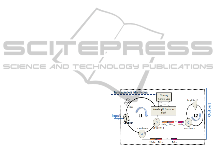
Organized in two loops as illustrated in Figure 1, the
virtual memory is used to buffer several signals
during different time duration. This memorization is
done by enclosing signals in the first loop, named
delay loop (L1 in Figure 1). When the power of a
signal reaches an unacceptable level, it is amplified
in the second loop, named amplification loop (L2 in
Figure 1). Implemented using all-optical
components, the virtual memory consists of an
optical combiner, an optical fiber, a wavelength
converters block, an optical amplifier, three
circulators and two FBG arrays.
Figure 1: Multi-wavelength virtual memory architecture.
The proposed architecture uses a relatively
reduced components number, according to existing
architecture. Moreover, the included components are
well known devices with reduced complexity
functioning. This criterion guarantees that the buffer
architecture is implementable.
The fiber inserted in the delay loop has a fixed
length L. This length can be assimilated to the first
loop length. The second loop encloses only the
amplifier, so its length can be considered as quasi
null. Each revolution signals are delayed by a time
duration
Δ
T proportional to the fiber length L; this
duration is named memory sensitivity. The total
delay accumulated by the k
th
signal after n
revolutions in the buffering block is equal to (n
Δ
T).
All-opticalMulti-wavelengthVirtualMemoryArchitecture-DesignandPerformancesAnalysis
389
The fiber length L must be proportional to the
slot duration S, which corresponds to the maximum
data unit length, to confine the total signals. The
physical implementation of the buffer takes the
maximum data unit length into account but remains
independent of each data unit length.
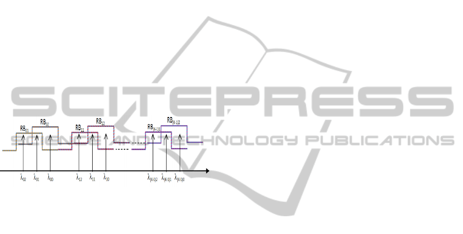
An array of FGBs (Srivastava et al., 2008) is
inserted at the virtual memory output path and a
second array is inserted between the delay loop and
the amplification loop. As the buffer can enclose K
signals at the same time, each array constitutes a
sequence of K reflection bands (RB): the array at the
output path constitutes the first sequence of K RB
named RB
k1
, k
∈
[0, K[ and the array between both
loops constitutes the second sequence of K RB
named RB
k2
, k
∈
[0, K[. As shown in Figure 2, the
RB
k1
and RB
k2
are overlapped and the K bands
consisting of the union of RB
k1
and RB
k2
are
disjointed one of the other.
Figure 2: Organization of the reflection bands sequences.
Signals arriving on the input path pass to the
delay loop throw the combiner. At this moment,
theirs wavelengths are in the band B
1
, it means that
each k
th
signal has as wavelength λ
k1
(∈ RB
k1
∩
RB
k2
), which corresponds to overlapping zone
between RB
k1
and RB
k2
. Having these wavelengths,
signals remain enclosed in the delay loop until theirs
wavelengths are converted. Signals pass throw the
optical fiber which induces a delay equal to
Δ
T each
revolution. Then, they pass throw the wavelength
converter block. The signal number k leaves the
converter block with wavelength equal to: λ
k1
if it
has to make another turn in the delay loop, λ
k2
(
∈
RB
k1
-(RB
k1
∩
RB
k2
)) if it has to be amplified and λ
k0
(
∈
RB
k2
-(RB
k1
∩
RB
k2
)) if it has to exit the buffering
block. Then, signals reach the first port of the first
circulator and they are led to its second port. The
signals pass throw the second FBGs array which
constitutes the reflection bands RB
k2
, k
∈
[0, K[. Two
cases may occur: signals with wavelengths out of the
RB
k2
, that means signals with wavelengths equal to
λ
k2
, are transmitted to the second circulator; but
signals with wavelengths inside the RB
k2
, that means
signals with wavelengths equal to λ
k1
or λ
k0
, are
reflected to the first circulator. The transmitted
signals arrive at the second port of the second
circulator and are led to its third port. So these
signals enter to the second loop where they are
amplified. Passing from the first port to the second
port of the second circulator, these signals leave the
amplification loop, cross the reflection bands RB
k2
and are led from the second port to the third port of
the first circulator. Also the reflected signals are led
from the second port to the third port of the first
circulator. Signals arriving at the first port of the
third circulator are led to its second port. Then, they
pass throw the first FBGs array which constitutes the
reflection bands RB
k1
, k
∈
[0, K[. As happen with the
first reflection bands, two cases may occur: signals
with wavelengths out of the RB
k1
, that means signals
with wavelengths equal to λ
k0
, are transmitted on the
virtual memory output path; but signals with
wavelengths inside the RB
k1
, meaning signals with
wavelengths equal to λ
k1
or λ
k2
, k
∈
[0, K[, are
reflected to the second port of the third circulator.
Transmitted to the third port of the third circulator,
the reflected signals reenter to the delay loop and are
passed by the combiner to the optical fiber. Signals
remain enclosed in the delay loop until the
wavelength converter block shifts theirs wavelengths
to: (a) λ
k2
and so they are passed to the amplification
loop, or (b) λ
k0
to be exited from the memory.
2.2 Wavelength Converter Block
A wavelength converter block is inserted inside the
delay loop. This block is used to convert the signals
wavelengths independently one of each other. In
fact, several signals can be enclosed in the virtual
memory at the same time (at most, K signals);
signals having to be amplified must have theirs
wavelengths converted to λ
k2
(k
∈
[0, K[); signals
which were just amplified, during the previous turn,
must have theirs wavelengths reconverted to λ
k1
(k
∈
[0, K[); signals having to exit the virtual memory
to the switching block must have theirs wavelengths
converted to λ
k0
(k
∈
[0, K[) and signals having to
turn again in the delay loop must have theirs
wavelengths maintained to λ
k1
(no conversions are
needed).
As shown in Figure 3, the wavelength converter
block consists in a set of K tunable wavelength
converter (Wang et al., 2006) managed by a memory
control unit. When signals turning in the delay loop
arrive at the wavelength converter block, a
demultiplexer separates them on K paths. On each
path an optical sensor is used to detect the arrival
moment of each signal. These sensors inform the
memory control unit of the arrival moment of
OPTICS2012-InternationalConferenceonOpticalCommunicationSystems
390
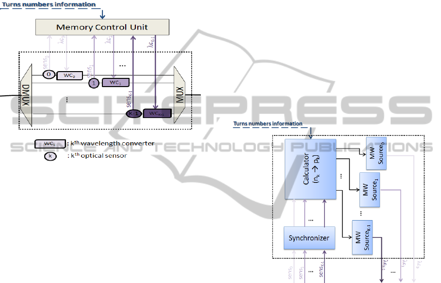
signals. Each sensor sends an information signal
named sens
k
, where k
∈
[0, K[ is the range of the
sensor. The wavelength converters make the needed
conversion or still idle according to the decision of
the memory control unit. The control unit generates
K control signals organized in an array of control
wavelength named
0..−1
. Then, the K paths
are regrouped by the multiplexer.
Figure 3: Wavelength converter block architecture.
2.3 Memory Control Unit
The control unit is the component that manages the
signals paths by delivering synchronous signals to
pilot the wavelength converters. According to the
previously received turn number information (sent
by a component upstream from the virtual memory),
it generates the three kinds of wavelengths
summarized in Equation 1 at different moments.
Using all-optical technologies, the control unit
consists of three main components as shown in
Figure 4: calculator, synchronizer and multi-
wavelength sources (MW sources).
The calculator receives the information about
required turn numbers for each enclosed signal.
According to the physical implementation of the
loops, it computes the amplifications number p
k
for
each signal. Each time a signal crosses the
wavelength converter block, the calculator is
advertised by the synchronizer and memorizes the
turn number for this signal. According to this
number, the calculator can let the k
th
MW source
ideal, if no conversions are required; also it can
generates a signal indicating to the MW Sources
k
,
k
∈
[0, K-1], which kind of wavelengths they must
generate (λ
k0
, λ
k1
, λ
k2
). So, the calculator has to
realize only two simple operations (increment and
comparison) which can be carried out in optical
domain.
The synchronizer is used to command the
calculator to start the signal generation exactly when
the k
th
signal arrives at the wavelength converter
block. In fact, at its arrival, signal crosses the k
th
optical sensor to inform the control unit of its
arrival. If a conversion is required, the control unit
must start generating a continuous wave intended for
the wavelength converter.
The MW sources are a set of multi-wavelength
laser sources generating the wavelengths required to
signal conversion. These components receive control
signals from the calculator, and generate the optical
continuous signals organized in the array of control
wavelength
0..−1
. The multi-wavelength
laser source can be chosen from the existing
components. However, its implementation should
pay attention to its response time, since it can affect
the system performances.
Figure 4: Memory control unit architecture.
Several technologies can be used to provide a
wavelength generator for the control unit. Among
the most important technologies, one can distinguish
two components; the optical flip-flop memory
(Kurobe et al., 2007) and the laser neural network
(Liu et al., 2004). Due to the described memory
control unit, the proposed virtual memory provides a
dynamical variable memorization time without
resort to electrical domain.
3 PERFORMANCES ANALYSIS
We evaluate performances of the system, and more
precisely of the buffering block, by assessing four
communication parameters: the delay, the
attenuation, the dispersion and the signal to noise
All-opticalMulti-wavelengthVirtualMemoryArchitecture-DesignandPerformancesAnalysis
391

ratio (SNR). In fact, each component crossed by
signals adds some delay and signal distortion.
For simplification reasons, we suppose that: (a)
the circulator and the combiner have identical effect
on signals independently of their input port; (b) all
used FBGs have the same effects on the
communication performances; (c) the dispersion
induced by the cross of the FBGs, the wavelength
converter block and the optical amplifier is
negligible according to the dispersion induced by the
other components; (d) only the optical amplifier and
the wavelength converter block in active mode
increase the noise.
In this work, n represents the turn number in the
delay loop. Each revolution, the crossed components
increase the signal distortion by increasing the
attenuation, the dispersion and the noise. After a
number of turns, the signals power reaches a critical
level. That’s why amplification must be performed.
After n turns in the memorization loop and p
turns in the amplification loop, the k
th
signal
cumulates the total delay given by equation 1, where
c, n
fib
and L are respectively the light celerity,
refractive index and fiber length; and the T
conv,on
,
T
conv,off
, T
FBG,ref
and T
FBG,trx
are respectively the
response times of the active wavelength converter,
the inactive wavelength converter, the reflecting
FBG and the transmitting FBG. One can see that the
delay induced by the optical fiber is the most
important one according to the delay of the
converter and the FBGs. So, the signal rang (k) has a
neglected effect on the cumulated delay.
()
() ( )
()( )( )
[]
,,
,,
,
21
21 21
212 1 21
fib
kn FBGref
vonv on vonv off
F
BG trx
fib
Ln
Tn npT
c
pT npT
knpKpT
Ln
n
c
=+−−
++ +−−
+− −−+ +
≈
(1)
Equation 2 evaluates the power attenuation occurred
to the k
th
signal after n turns in the memorization
loop and p turns in the amplification loop. In this
equation, A
comb
, A
fib
, A
cir
, A
conv,on
, A
conv,off
, A
FBG,ref
and
A
FBG,trx
, respectively appoint the attenuation of the
combiner, fiber, circulator, wavelength convertor in
active mode, wavelength convertor in inactive mode,
FBG when signals are reflected and the FBG when
signals are transmitted. The G
amp
is the optical
amplifier gain.
()
[]
,
,,
,
,
(4 2 1)
(2 1) ( 2 1)
(2 1)
2 ( 1) ( 2 1) (2 1)
kn comb fib cir
conv on conv off
FBG ref amp
F
BG trx
AnA AL npA
pA npA
np A pG
knpKpA
=+++−
++ +−−
+−− −
+ − −−+ +
(2)
The accumulated dispersion is given by equation 3
for the k
th
signal after n turns in the memorization
loop and p turns in the amplification loop. The
symbols D
comb
, D
fib
and D
cir
give respectively the
dispersion of the combiner, fiber and circulator. The
Δ
λ is the spectral line width of the laser source.
(
)
cirfibcombnk
DpnLDDnD )124(
,
−++Δ+=
λ
(3)
The equation 4 listed below gives the SNR
expression after n turns in the memorization loop,
inducing a cascade of p amplifications and (2p+1)
wavelength conversions, where P
in
is the input
signal power, SNR
conv,on
is the SNR introduced by
the wavelength converter in active mode, η
SP
is the
ratio of electrons in higher and lower states, h is the
Plank’s constant,
∇
f is the bandwidth that measures
the noise figure and G
amp
is the optical amplifier
gain.
[]
inonconvkampsp
onconvin
nk
PpSNRGfhp
SNRP
SNR
)12()1(2
,
,
,
++−∇
=
λη
(4)
4 SIMULATIONS AND RESULTS
4.1 Simulation Model and
Parameterization
To demonstrate the proposed memorization
function, a multi-wavelength model implemented
using the OptiSystem simulator and Matlab is
presented in this section. The laser sources are
modeled as pseudo-random bit sequence generators
with variable data unit size. Mach-Zehnder
modulators are used with continuous wave lasers
having a power of 1mW, and NRZ generators. The
wavelength converter block is represented by
developed Matbab co-simulator components. The
FBG arrays are modeled by subsystems of FBGs.
The optical receivers are modeled as PIN
photodetectors and low pass Bessel filters. The data
unit size is fixed to 1500 bytes.
To evaluate the performances limits of the
system, we need to implement the worst case, which
means, when all the transmitters generate signals
having to be enclosed in the buffering block for the
maximum time duration.
A set of simulations is performed for several
buffering fiber length, capacity and bit rate values.
The variations of the delay, attenuation, dispersion
and SNR while the turn number is increasing are
collected from the list of signal port data of the
simulation model layout at the output ports. After
OPTICS2012-InternationalConferenceonOpticalCommunicationSystems
392
receptions, signals are translated to electrical domain
and analyzers show their eye diagram and calculate
the maximum Q factor.
4.2 Results Analysis
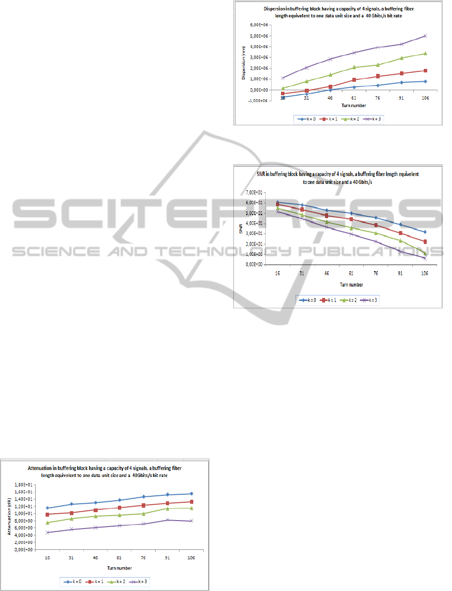
To evaluate the communication parameters variation
in function of the turn number and the signal rank, a
first set of simulations is performed where the
buffering fiber length is fixed to be equivalent to one
data unit size (59,95m), the buffering capacity is
equal to four wavelengths and the system bit rate is
40 Gbits/s. The attenuation, the dispersion and the
SNR of each signal is depicted while the turn
number is increasing.
By examining the curves of Figure 5, one can say
that the attenuation depends of the signal rank (k). In
fact, as previously illustrated in equation 6, the
number of crossed FBG depends of the signal rank.
Also, this variation can be explained by the effect of
the amplifier on each signal according to its
wavelength value.
Figure 6 illustrates the variation of the dispersion
while the turn number is increasing for the different
signal ranks. It is evident that when turn number
increases, the dispersion increases also, as the
number of crossed equipments increases. As the
fiber, one of most equipment affecting the signal
dispersion, adds varied dispersion on signals
according to theirs wavelengths, the signal
dispersions depend of the signal ranks.
The SNR variation of each signal when turn
number is growing is depicted in Figure 7. As each p
turns in the first loop, signals have theirs
wavelengths converted and are amplified, it is clear
that the SNR value decreases. As the amplifier
contribution in the SNR depends of the signal
wavelength value, curves in Figure 7 are
distinguishable.
Figure 5: Variation of the attenuation for various turn
number and signal ranks.
Figure 6: Variation of the dispersion for various turn
numbers and signal ranks.
Figure 7: Variation of the SNR for various turn numbers
and signal ranks.
To evaluate the effect of the architecture
characteristics on signals quality, three simulation
sets are performed by fixing two characteristics and
varying a third one: the system bit rate, the buffering
fiber length and buffering capacity. Firstly, the
buffering fiber length and the buffering capacity are
fixed respectively to the equivalent one data unit
size (1500 bytes) and four wavelengths and the
system bit rate is varied to 2,5, 10 and 40 Gbits/s,
secondly, the capacity and bit rate are fixed
respectively to four wavelengths and 40 Gbits/s and
the buffering fiber length is varied to the equivalent
of 1, 5 and 10 data unit length, and thirdly, the bit
rate and the buffering fiber length are fixed to 40
Gbits/S and the equivalent of one data unit length
(59,95 m) and the buffering capacity is varied to
one, two, four and height wavelengths. The
maximum Q factor is depicted for each signal while
the turn number is increasing. Then, the maximum Q
factor average is calculated.
In Figure 8, the maximum Q factor average
variation for several system bit rates is showed. One
can see that the signal quality decreases when the
turn number growth. But it remains in acceptable
All-opticalMulti-wavelengthVirtualMemoryArchitecture-DesignandPerformancesAnalysis
393
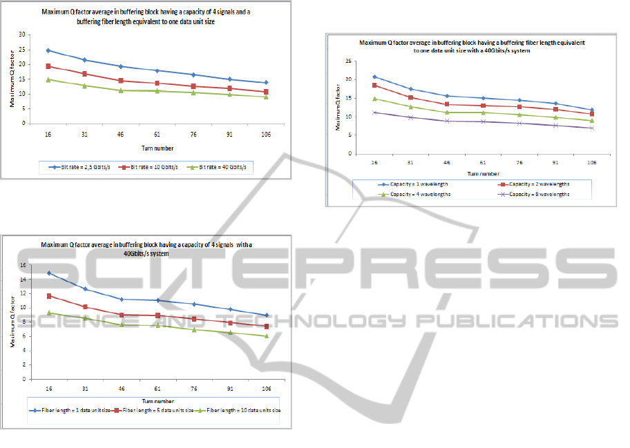
row for the three bit rates.
Figure 8: Maximum Q factor average variation for various
system bit rates.
Figure 9: Maximum Q factor average variation for various
buffering fiber lengths.
The Maximum Q factor average variation for
several buffering fiber lengths is illustrated in Figure
9. While the fiber length (size of the delay loop) is
growing, it degrades the signal quality. This fact can
be explained by the attenuation and dispersion rising
when the crossed fiber length increases.
Figure 10 shows the Maximum Q factor average
variation for several buffering capacities. Curves
prove that the buffering capacity decreases the
signals quality while increasing. This fact can be
justified by the crosstalk effect of signals one on
another.
Architecture presented in (Park et al., 2008)
operates at 40Gbits/s with a single wavelength
capacity and 9cm fibre length. After one turn, signal
is delayed by 1.1ns with a power penalty of 2.4dB
and a Q factor of 6. Authors predict that the
architecture is able to achieve 9 or 10 recirculations
with the same power penalty. To obtain more delay,
using a longer delay line requires the insertion of
amplification inside the delay line.
As our architecture includes amplifications only
when needed, in 40Gbits/s system and with four
wavelengths capacity, it is able to delay signals for
more than 30μs with a Q factor average of 8.
Figure 10: Maximum Q factor average variation for
various buffering capacities.
To summarize, one can say that simulations
prove that the proposed all-optical multi-wavelength
virtual memory is able to memorize several data
units having variable sizes in scalable bit rate
systems. Due to the simulation limits, no simulations
for more than 8 wavelengths as buffering capacity
were performed. However, using the aggregation of
several virtual memories can provide an important
number of memorized signals.
5 CONCLUSIONS
This work presents a novel architecture of an all-
optical multi-wavelength virtual memory based on
tunable wavelength converter and FBGs. The
architecture is organized in two loops: the first loop
encloses the signals during the buffering time, and
the second one amplifies the signal optical powers
just when they reach a critical level. Several signals
can be memorized at the same time and the entrance
and the exit of each one is managed independently
of the others. The proposition includes all-optical
control parts making the virtual memory
independent of external events. All decisions are
made according to required turn number for each
signal calculated on the base of previously received
information. The feasibility of this proposition is
demonstrated by analyzing the performances of the
buffering block. This analysis is confirmed by
simulation studies. Our architecture can memorize
an important number of signals at the same time
with a fine response time (sensitivity) quasi equal to
the data unit duration
Δ
T in a system of 40Gbits/s
with a relatively acceptable signal distortion.
OPTICS2012-InternationalConferenceonOpticalCommunicationSystems
394

The all-optical multi-wavelength virtual memory
can be implemented inside a switching node to be
used as a solution to various traffic engineering
tasks. Several traffic engineering applications can be
addressed in optical burst switching network such
as: contention resolution, delay based quality of
service (QoS) provision, call admission control and
congestion control.
REFERENCES
Batti, S., Zghal, M., Boudriga, N., Hall, T., 2009. An all-
optical synchronizer for switching node using single-
sideband modulator and fiber Bragg gratings. In ISCC,
Tunisia, 5-8 July.
Batti, S., Zghal, M., Boudriga, N., 2010. A new all-optical
switching node including virtual memory and
synchronizer. In Journal of Networks, 5(2), pp. 165-
179.
Burmeister, E.F., Blumenthal, D.J., Bowers, J.E., 2008. A
comparison of optical buffering technologies. In
Optical Switching and Networking, 5(1), pp. 10-18.
Kurobe, T., Kimoto, T., Muranushi, K., Kagimoto, T.,
Kagi, N., Kasukawa, A., Wu, J., Otani, E., Arimoto,
H., Tsuji, S., 2007. Tunable laser source for fast
wavelength switching using a short-cavity DBR laser
packaged with wavelength locker. In National Fiber
Optic Engineers Conference, 25-29 March.
LeGrange, J. D., Bernasconi, P., Simsarian, J. E., Neilson,
D. T., Stiliadis, D., Gripp, J., Zirngibl, M., 2007.
Demonstration of a time buffer for an all-optical
packet router. In Journal of Optical Networking, 6(8),
pp. 975-983.
Liu, Y., Hill, M.T., Geldenhuys, R., Canbretta, N., de
Waardt, H., Khoe, G,D., Dorren, J.S., 2004.
Demonstration of a variable optical delay for a
recirculating buffer by using all-optical signal
processing. In IEEE Photonics Technology Letters,
16(7), pp. 1748-1750.
Mack, J.P., Burmeister, E.F., Garcia, J.M., Poulsen, H.N.,
Biljana Stamenic, Kurczveil, G., Nguyen, K.N.,
Hollar, K.,Bowers, J.E., Blumenthal, D.J., 2010.
Synchronous optical packet buffers. In, IEEE Journal
of Selected Topics in Quantum Electronics, 16(5), pp.
1413-1421.
Park, H., Mack, J. P., Blumenthal, D. J., Bowers, J. E.,
2008. An integrated recirculating optical buffer. In
Optical Express, 16, pp. 11124-11131.
Srivastava, R., Singh, R. K., Singh, Y. N., 2008. Fiber-
optic switch based on fiber Bragg gratings. In IEEE
Photonics Technology Letters, 20(18), pp. 1581-1583.
Wang, J., Sun, J., Kurz, J. R., Fejer, M. M., 2006. Tunable
wavelength conversion of ps-pulses exploiting
cascaded sum- and difference frequency generation in
a PPLN-fiber ring laser. In IEEE Photonics
Technology Letters, 18(20), pp. 2093-2095.
All-opticalMulti-wavelengthVirtualMemoryArchitecture-DesignandPerformancesAnalysis
395
