A 0.18µm CMOS 2nd Order Sigma-Delta Modulator for Low-power
Biosensor Applications
Ryan Selby and Tom Chen
Department of Electrical and Computer Engineering, Colorado State University, Fort Collins, CO, U.S.A.
Keywords:
Sigma-Delta Modulator, Biosensor.
Abstract:
Silicon biosensors are becoming increasingly popular for the study of cell growth and movement in biological
systems. These biosensors need small, low power, highly accurate sensors and analog to digital converters
(ADCs) in order to generate chemical images of small tissue samples. Low-power and low-voltage design is
key in battery operated systems, and the size of the circuits need to be kept small such that arrays of sensors
can be placed on each chip. This paper presents a low-voltage, low-power, 2nd order Sigma-Delta modulator
for use in an electrochemical biosensor system. The modulator was designed using a commercial 0.18µm
CMOS process with a supply voltage of 0.9V. With an input signal bandwidth of 1kHz it achieves a SNDR
of 61.2dB using an over-sampling ratio of 500. Power dissipation is 165µW and it occupies 0.0225mm
2
of
silicon area.
1 INTRODUCTION
Integrated silicon biosensors have been proposed as a
method for detecting chemical levels within biologi-
cal systems (Pettine, 2012). One application for these
biosensors is the study of cell movement and devel-
opment within brain tissue. Using electrochemistry
for signal detection, an array of micro-electrodes in
such a biosensor would be able to measure chemical
gradients across small pieces of living tissue. These
gradients form a chemical image. Current methods
for creating chemical images involve dye and mark-
ing compounds which could kill the tissue sample.
The traditional methods of observing cell movement
and changes are not ideal because temporal changes
in chemical concentrations and cell movement cannot
be observed reliably. An integrated silicon biosensor
array of hundreds or thousands of electrodes would
solve these problems by measuring chemical levels
in live tissue, allowing scientists to observe important
changes over time.
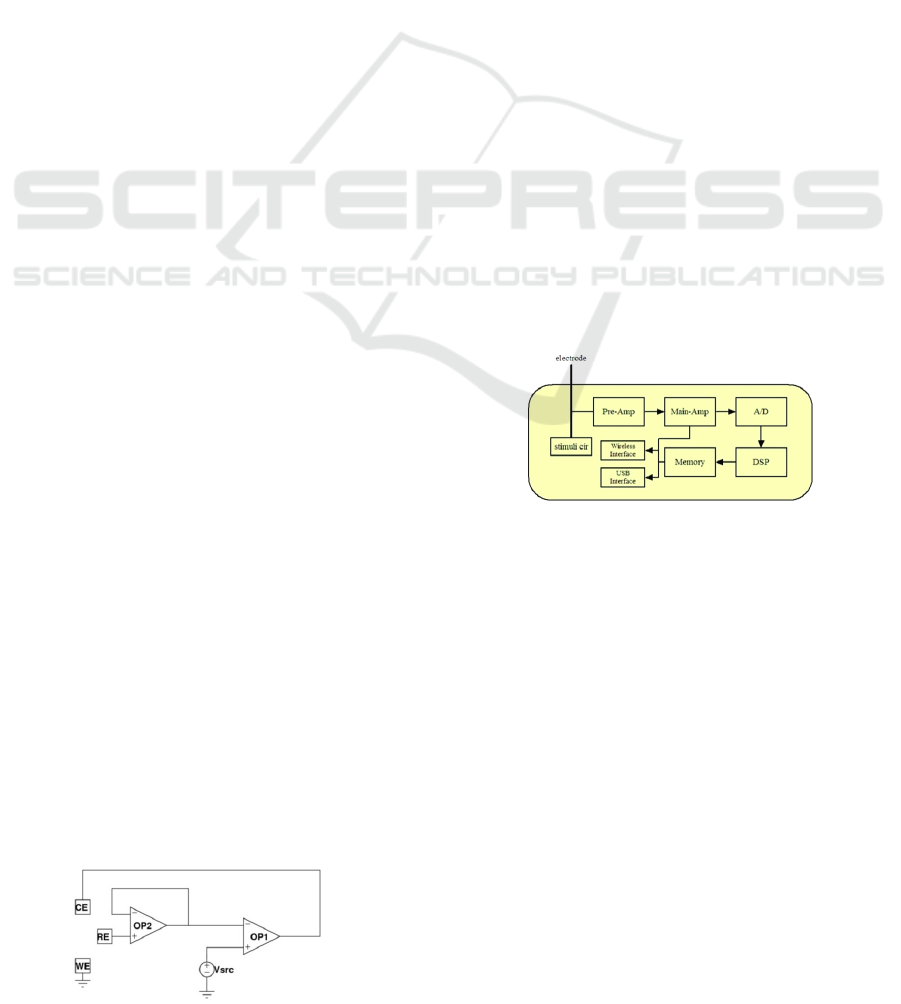
Figure 1: Potentiostat schematic.
Figure 2: The top-level schematic of the biosensor system.
Nitric oxide (NO) is a chemical that is believed
to influence cell movement and growth in brain tis-
sue. This chemical is electrochemically active and
can be measured using electrochemical methods im-
plemented in a silicon biosensor. In order to create the
chemical image of the NO in the tissue, many circuit
components are needed. First, a potentiostat is used to
induce a current in the tissue sample proportional to
the concentration of nitric oxide. A low power design
of the integrated potentiostat for this system can be
found in (Duwe, 2011). The induced currents are ex-
tremely small, on the order of tens of picoamps, and
need to be converted to voltage signals and amplified
by way of a transimpedance amplifier. Finally, main
amplifiers and an analog to digital converter (ADC)
further amplify the signal and convert it to a digi-
tal value. A low power bit-serial decimator design
that interfaces with the modulator presented in this
paper can be found in (Scholfield, 2012). Figure 1
shows the electrode arrangement and potentiostat cir-
cuit proposed in (Duwe, 2011), and Figure 2 shows
5
Selby R. and Chen T..
A 0.18µm CMOS 2nd Order Sigma-Delta Modulator for Low-power Biosensor Applications.
DOI: 10.5220/0004187100050009
In Proceedings of the International Conference on Biomedical Electronics and Devices (BIODEVICES-2013), pages 5-9
ISBN: 978-989-8565-34-1
Copyright
c
2013 SCITEPRESS (Science and Technology Publications, Lda.)
the top-level schematic of the biosensor system.
In order to create an accurate chemical image, the
electrodes need to be spaced at distances comparable
to the size of individual cells within the tissue sam-
ple. Electrode pitches of 10µm to 25µm are desirable.
Ideally, each electrode should have its own dedicated
circuitry; however with the extremely small electrode
pitch this is not realistic. Regardless, minimizing
the area of the circuitry is important to reduce the
number of shared electrodes per circuit block. Like-
wise, power consumption should be minimized since
the biosensor will contain many copies of the detec-
tion circuitry running in parallel. Power consumption
must also be limited to avoid heat build-up within the
tissue, possibly causing damage.
The chemical signals detected with the potentio-
stat typically have very low bandwidths; nitric ox-
ide signals do not normally exceed 1 kHz. While
bandwidth requirements are low, measurement ac-
curacy is much more important. Noise and signal
distortion must be avoided to preserve the integrity
of the small signals inherent in bio-electric systems.
Sigma-Delta ADCs are ideal for biosensor applica-
tions because they inherently have higher resolution
and lower bandwidth than other ADC topologies.
Many different designs for low-power Sigma-
Delta Modulators have been presented. The de-
signs in both (Zhang, 2010) and (Jasutkar, 2011) are
based on 0.18µm CMOS processes with nominal 1.8V
power supplies. These designs use standard archi-
tectures and standard techniques for reducing power.
The design in (Zhang, 2010) was intended for au-
dio applications, while (Jasutkar, 2011) presents a
design for biomedical applications such as electo-
cardiograms. The designs presented in (Goes, 2006)
and (Lee, 2006) also use 0.18µm CMOS processes
but they use supply voltages of 0.9V and 0.8V re-
spectively to reduce power. Besides lowering the sup-
ply voltage, these designs modify the standard archi-
tecture to save power. (Goes, 2006) shares a single
op-amp between multiple integrator stages and (Lee,
2006) is able to be used at different speeds depending
on the application to maximize efficiency. The design
presented in this paper explores the efficiency of using
a reduced power supply to lower power consumption
while still using a standard, easy to implement archi-
tecture.
All of these designs are also fully differential ar-
chitectures while the proposed design is single ended.
The use of differential design has the advantage of
expanded output range; however, our application fo-
cuses on NO which has a narrow activation range.
Therefore, a single-ended design is chosen for re-
duced silicon area. In switched-capacitor circuits
where capacitors can occupy a large percentage of the
total area, this is critical. Section II of the paper will
detail the design of the modulator and its components,
and Section III will cover the proposed physical lay-
out and present simulation results.
2 PROPOSED LOW POWER
MODULATOR DESIGN
2.1 Top Level Design
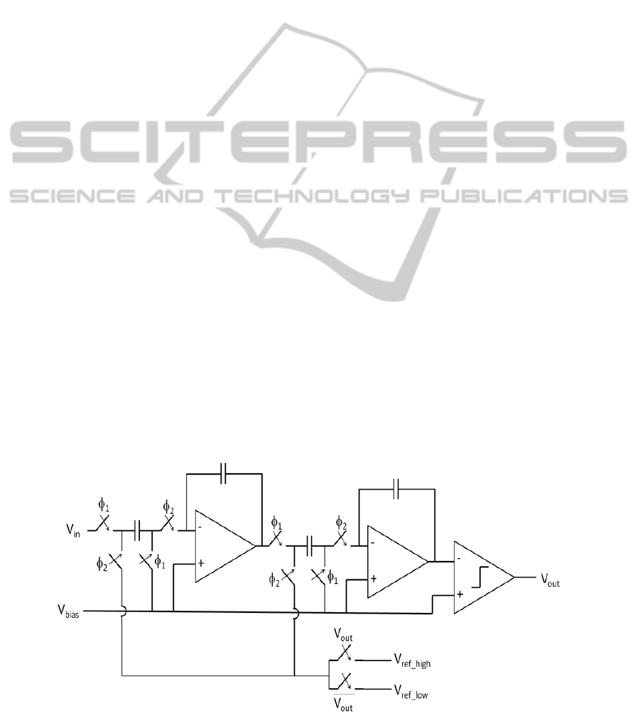
The overall block level diagram of the proposed mod-
ulator is shown in Figure 3. The design is imple-
mented using a standard 0.18µm silicon process and
a supply voltage of 900mV. The overall topology is
a single ended, second order, Sigma-Delta modulator.
This topology uses two integrators, a comparator, and
a 1bit DAC to provide feedback. With accuracy and
Figure 3: Top level modulator schematic.
BIODEVICES2013-InternationalConferenceonBiomedicalElectronicsandDevices
6
Figure 4: Op-amp schematic.
power consumption prime concerns in this design, the
modulator is implemented using switched capacitors
which both improve matching in the integration stages
and allows for lower power consumption than a con-
tinuous time resistive implementation.
The bio-chemical signals the chip will be mea-
suring have a maximum bandwidth of 1kHz which
makes a Sigma-Delta based ADC with a large over-
sampling ratio ideal for accurate measurements. The
input is sampled at 1MHz resulting in an oversam-
pling ratio of 500. This clock frequency was chosen
based on the performance requirements of the deci-
mation filter presented in [3], and power consumption
was reduced as much as possible using this sampling
rate.
2.2 Modulator Op-amp Design
The schematic for the proposed op-amp is shown in
Figure 4. The nominal supply voltage used with this
process is 1.8V because the threshold voltages of the
nFETs and pFETs available in this process are ap-
proximately 450mV and -400mV respectively. When
designing with a 900mV supply, cascoding transistors
is not practical in most situations. Thus the op-amp
uses multiple, simple, stages to achieve high gain.
The design features three stages comprised of a
differential pair input followed by common source
amplifiers and current mirrors. Adding extra stages to
an op-amp inherently leads to stability problems, and
thus two large compensation capacitors are needed to
maintain a reasonable phase margin. Capacitors C1
and C2 in the schematic have values of 3.6pF and
1.3pF respectively. Because of the relatively large
values of the compensation capacitors they are imple-
mented on using poly/n-well capacitors. These capac-
itors are used because they are much more area effi-
cient than standard metal/poly capacitors. The differ-
ential pair uses pFETs for the input to reduce noise,
and the input/output common mode voltage is set to
175mV. With the limited supply voltage, the maxi-
mum peak-to-peak output swing is 300mV. Internal
biasing voltages for nMOS and pMOS devices are
generated using simple current mirrors with resistors
generating the reference currents. The resistors are
implemented as thin-film devices which are more area
efficient and more accurate than other resistor tech-
nologies. Monte Carlo simulations have shown that
these bias voltages do not vary widely enough to im-
pact the functionality of the op-amp.
Small bias currents were used throughout the op-
amp to reduce power consumption. All branches in
the op-amp use 10µA bias currents except the output
stage which uses 30µA to aid in stability. In total, the
op-amp uses 70µA of current and consumes 63µW.
The proposed design has a DC gain of 112dB, 8.3Hz
-3dB bandwidth, and a phase margin of 77 degrees.
2.3 Integrator
The proposed modulator uses two switched capacitor
integrators which each use a 100fF sampling capaci-
tor and 4pF feedback capacitor. The sampling capac-
itor uses bottom plate sampling to reduce error due to
charge injection. The ratio of feedback capacitance to
sampling capacitance is set to 40:1 to prevent the out-
put of the first modulator from saturating. Using this
ratio the output of the first modulator uses the entire
300mV peak-to-peak output swing range of the op-
amp. The capacitance ratio of the second integrator
was set to 2:1, which allowed the second integrator to
use its full output range as well.
A0.18µmCMOS2ndOrderSigma-DeltaModulatorforLow-powerBiosensorApplications
7
While the capacitance ratio is determined by the
output swing requirements of the op-amps, the ab-
solute sizes of the capacitors are chosen based on a
compromise between noise characteristics and physi-
cal size when implemented on chip. The 100fF input
capacitor was chosen because it is the smallest value
possible which meets the thermal noise requirements
of the ADC system.
The sampling capacitor uses a poly/metal capaci-
tor which is extremely linear but also very large. The
feedback capacitor, which is much larger, is imple-
mented with a poly/n-well capacitor which has non-
linear properties yet is very area efficient. Obviously,
using different types of capacitors makes matching
more difficult, but the savings in area is considerable
compared to using two poly/metal capacitors. Poly/n-
well capacitors are roughly nine times smaller than
poly/metal capacitors.
2.4 Comparator Design
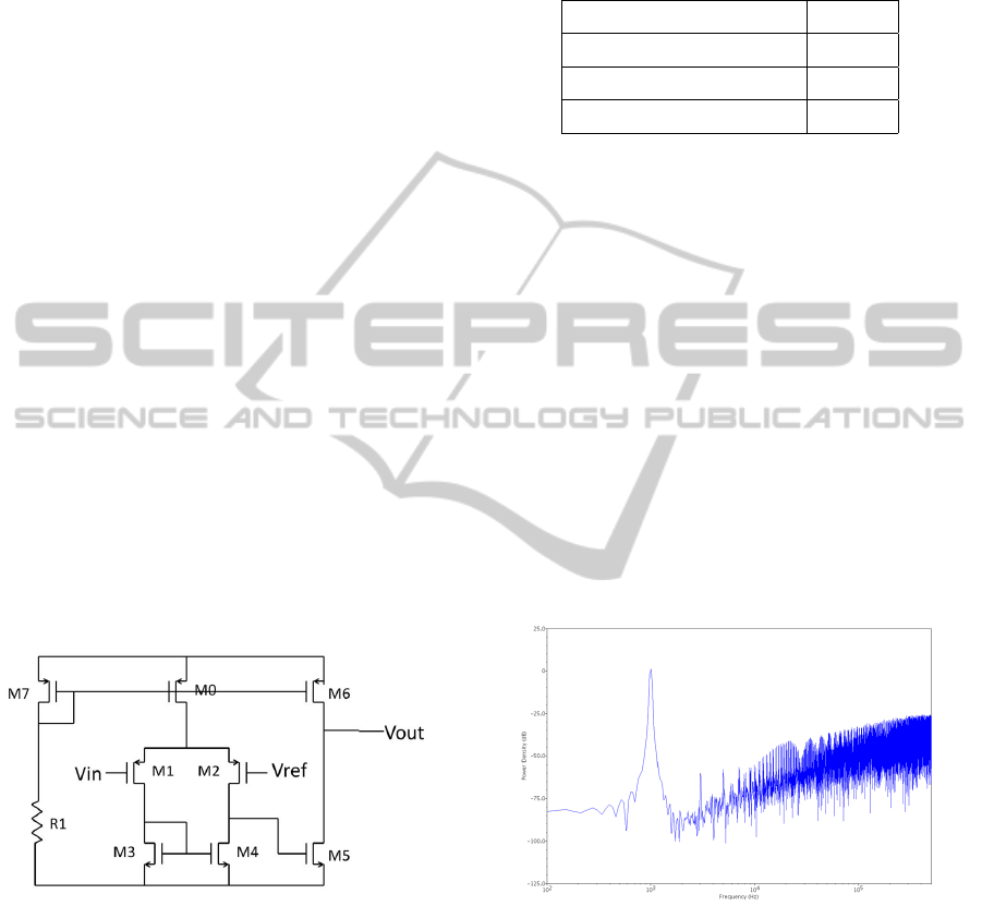
The schematic for the comparator is shown in Figure
5. The comparator uses the same differential pair as
the op-amp for an input stage, followed by a high gain
common source output stage. After amplifying the
input signal the digital output is latched by a simple
master-slave D flip-flop. The comparator uses 40µA
of DC current and consumes 36µW. The output of the
comparator settles to its final value within 10ns of the
latch closing.
Figure 5: Comparator schematic.
3 PHYSICAL IMPLEMENTATION
AND MEASUREMENT
RESULTS
Overall simulation results for the modulator are
shown in Table 1 while the power spectrum density
plot is shown in Figure 6. This plot shows regular
noise spikes at the 3rd harmonic and above of the in-
put tone which are easily filtered out by the low-pass
filter characteristics of the decimation filter. The mod-
ulator achieves a SNDR of 61.2dB resulting in a 10 bit
effective resolution while consuming 165µW.
Table 1: Modulator performance.
Parameter Results
SNDR 61.2dB
Effective Number of Bits 10
Power Consumption 165µW
The physical layout of the modulator covers an
area of 0.0225mm
2
. Many measures were taken to
ensure that transistor mismatch and signal distortion
were minimized throughout the layout. All matched
transistors in the op-amps and comparator were im-
plemented using common centroid layout techniques,
and all analog transistor blocks are surrounded by
guard rings. The 4 phase, non-overlapping clock gen-
eration circuit is also isolated via a guard ring. Fi-
nally, wires carrying important digital and analog sig-
nals throughout the chip are isolated with grounded
lines to minimize interference and crosstalk.
The proposed modulator was fabricated and its
functionality verified on silicon. An oscilloscope
screen capture in Figure 7 shows the modulator per-
forming as expected with a 1 kHz sine wave input. A
die photo of the test chip is shown in Figure 8.
Figure 6: Modulator output spectrum.
4 CONCLUSIONS
A low power, second order, Sigma-Delta modulator
for use in an integrated biosensor system was pre-
sented in this paper. The proposed modulator uses
a 900mV supply voltage to reduce power consump-
tion and extend the life of battery powered biosen-
sors. The modulator achieves a signal-to-noise distor-
tion ratio of 61.2dB and consumes 165µW. Compared
BIODEVICES2013-InternationalConferenceonBiomedicalElectronicsandDevices
8
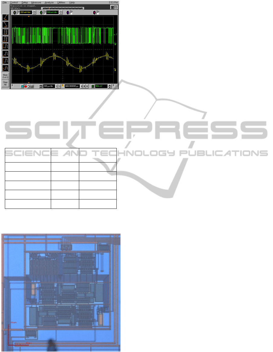
Figure 7: Silicon test results.
to existing low-power designs the proposed modula-
tor performs very well balancing SNDR and power
consumption. Table 2 compares the performance of
the proposed modulator against existing designs.
Table 2: Performance comparison.
Design SNDR
Proposed
Auto-zeroed
(Lei, 2010) 68.85dB 800µW
(Jasutkar, 2011) 68dB 400µW*
(Goes, 2006) 80.1dB 200µW
(Lee, 2006) 50dB 180µW
This Work 61.2dB 165µW
*(Jasutkar, 2011) quoted power consumption as 400W, corrected to 400µW
here.
Figure 8: Die photo.
REFERENCES
Duwe, M., Chen, T., ”Low power integrated potentiostat
design for µelectrodes with improved accuracy,” 2011
IEEE 54th International Midwest Symposium on Cir-
cuits and Systems (MWSCAS), pp.1-4, 7-10 Aug. 2011
Goes, J., Vaz, B., Monteiro, R., Paulino, N., A 0.9-V Delta-
Sigma modulator with 80 dB SNDR and 83 dB DR
using a single-phase technique, IEEE Int. Solid-State
Circuits Conf. 2006 Dig. Tech. Papers, pp. 191-200.
Jasutkar, R. W., Bajaj, P. R., Deshmukh, A. Y., GA Based
Low Power Sigma Delta Modulator for Biomedical
Applications, Recent Advances in Intelligent Com-
putational Systems, 2011 IEEE, pp. 772-776, 22-24
September 2011
Lee, S., Cheng, C., A Low-Voltage and Low-Power Adap-
tive Switched Current Sigma-Delta ADC for Bio-
Acquisition Microsystems, Circuits and Systems I,
Vol. 53, No.12, pp. 2628-2636, Dec 2006.
Lei, Z., Xian-li, Z., Xing-hua, W., Ruo-Yuan, Q., Two-order
Low-power Sigma-delta Modulator with SC Tech-
niques, Semiconductor Electronics, 2010 IEEE Inter-
national Conference on, pp. 96-99, 28-30 June 2010
Pettine, W., Jibson, M., Chen, T., Tobet, S., Henry, C.,
”Characterization of Novel Microelectrode Geome-
tries for Detection of Neurotransmitters,” Sensors
Journal, IEEE, vol. 12, no. 5, pp. 1187-1192, 2012
Scholfield, K., Chen, T., Low power decimator design us-
ing bit-serial architecture for biomedical applications,
Proc. of DATICS-IMECS 2012, March 14-16, Hong
Kong.
A0.18µmCMOS2ndOrderSigma-DeltaModulatorforLow-powerBiosensorApplications
9
